A Low Profile Polarization-insensitive Multiple-band Metamaterial Absorber using a Slotted Octagonal Unit Cell
Mohamed Elhefnawy, KyoungHun Kim, Tae-Hyeon Kim, and Wang-Sang Lee
1Department of Electronic Engineering
Gyeongsang National University, Jinju, 52828, South Korea
wsang@gnu.ac.kr
2Department of Electrical Engineering
October 6 University, Egypt
Submitted On: March 13, 2024; Accepted On: June 18, 2024
ABSTRACT
This paper introduces a thin, polarization-insensitive (PI), and multiple-band electromagnetic metamaterial absorber (MMA). The unit cell of the MMA consists of a slotted octagonal metallic patch printed on an FR4 dielectric substrate, backed by a grounded metallic layer, and notably does not incorporate resistive lumped elements. The proposed MMA exhibits measured absorption, exceeding 75% for normal incidence, across frequency bands ranging from 2.22–2.38 GHz, 6.86–7.24 GHz, 11.68–12.71 GHz, 14.1–14.8 GHz, and 15.47–16 GHz. The proposed MMA unit cell has dimensions of 0.21 0.21 and a thickness of 0.001, where represents the wavelength corresponding to the lowest frequency at 2.22 GHz. The performance of the proposed MMA is simulated using CST Microwave Studio and MATLAB, and subsequently validated through experimental measurements.
Index Terms: Absorption, metamaterial absorber (MMA), metasurface absorber, polarization-insensitive (PI), transmission line (TL) model.
I. INTRODUCTION
Absorbers are commonly utilized in various applications, including stealth technology and anechoic chambers. The wedge-tapered absorber is the most commonly used type of electromagnetic absorber, often employed in anechoic chambers. However, this pyramid-shaped array absorber is susceptible to damage and has large dimensions [1]. One of the most widely used absorbers is the Salisbury absorber, which is composed of three layers. The first layer consists of a thin resistive sheet, the middle layer is a low-loss dielectric with a thickness equal to an odd multiple of the quarter wavelength, and the bottom layer is a perfect electric conductor (PEC) located behind the dielectric slab. The odd multiples of the quarter-wavelength thickness of the dielectric material result in the transformation of a short circuit at the bottom layer into an open circuit at the top resistive layer. The effective impedance of the Salisbury structure is determined by the impedance of the top resistive layer. Impedance matching occurs when the impedance of the resistive layer matches that of free space. However, the Salisbury screen is limited by two primary constraints: its thickness and operational bandwidth. Furthermore, the Salisbury absorber maintains a bulky structure, especially when operating at lower frequencies. To address the problem of limited bandwidth, the Jaumann absorber has been developed to provide a wider absorption bandwidth by using a multi-layered design, while still maintaining a significant thickness similar to previous absorbers. The circuit analog absorber (CAA) consists of a periodic arrangement of conductive metal instead of a resistive sheet. The challenge of thickness persists in the CAA due to the middle layer’s thickness being approximately one-quarter of the wavelength. Metamaterials can be used as absorbers because they have the potential to effectively prevent the reflection and transmission of incident waves within specific frequency bands and polarizations. The metamaterial absorber (MMA) consists of periodic unit cells, with each cell comprising a dielectric substrate positioned between a top metallic layer and a ground layer at the bottom [2, 3, 4]. MMA may exhibit negative permeability and permittivity, or a negative refractive index. The negligible transmission through the absorber is attributed to the existence of a copper ground at the bottom of each unit cell [5]. The thin structure of the metamaterial can be classified as a metasurface [6]. Metasurface absorbers exhibit unique characteristics due to their artificial sub-wavelength structure. In the metasurface configuration, the surface currents present on the top resonance layer induce an electric resonance. Furthermore, the top resonance structure has the ability to interact with the ground layer, leading to the creation of anti-parallel currents that produce magnetic resonance [7]. The permittivity and permeability can be manipulated by utilizing the induced electric and magnetic resonances, respectively. As a result, it is possible to achieve impedance matching between the metasurface absorber and free space [8, 9]. There are many approaches that can be used to enhance the bandwidth of the electromagnetic absorber. One strategy is to incorporate lossy materials, such as resistive sheets, lumped resistors, or high-loss substrates. Another approach is to introduce multiple absorption bands and combine them to create a broader absorption bandwidth. Additionally, the pin diodes can be integrated with electromagnetic absorbers to switch between different frequency bands. For instance, in [10], a wide fractional bandwidth absorber was constructed by symmetrically placing eight 100 chip resistors along a 16-sided loop. Notably, there is a gap between the substrate layer and the ground in this configuration. In [11], the unit cell of the periodic structure contains two bow-tie dipoles, along with an additional resistive load. In [12], a low-profile absorber with ultrawideband capabilities was developed by incorporating a resistive frequency selective surface (FSS) layer on a ground-backed substrate. The utilization of single- and double-layer resistive FSS was introduced in [13]. Additionally, a design for an absorber using concentric circular rings loaded with lumped resistances was presented in [14]. A low-cost, extremely thin, and angularly stable metallic high-impedance FSS absorber was presented in [15]. In [16], a configuration of three interconnected hexagonal split-ring resonators was introduced to create an MMA with a negative refractive index. Additionally, the design of metamaterial unit cells with matching permittivity and permeability was presented in [17] to generate an absorber with an impedance equal to that of free space. In [18], a periodic arrangement of double-split ring resonators was presented. This MMA demonstrated the ability to absorb electromagnetic waves regardless of their polarization. The relative permeability was controlled by inducing magnetic resonance, which was caused by the generation of surface currents flowing in opposite directions between the top and bottom layers. Furthermore, the dielectric constant was manipulated by the induced electric field in the capacitive gap on the top layer. In [19], it was observed that the intense concentration of electromagnetic fields leads to the absence of reflection, causing the incident EM wave to be absorbed. In [20], two FSS layers positioned on either side of a dielectric substrate were utilized to create a dual-sided absorber. In [21], an ultra-thin MMA was designed to minimize the in-band radar cross-section (RCS) of a waveguide slot antenna. This absorber comprised two metal layers separated by a lossy dielectric spacer. The top layer consisted of an etched oblique cross-gap patch arranged in a periodic pattern, while the bottom layer was made of solid metal. Additionally, in [22], a C-band microwave absorber based on complementary split-ring resonators (CSRR) was introduced. In [23], the FSS unit cell design allows for the integration of PIN diodes between neighboring unit cells to facilitate switching between the X-band and C-band for RF shielding applications.
This research presents a novel MMA design, notable for its capacity to support a greater number of frequency bands when compared to designs of similar size and low profile. Unlike prior studies that relied on complex structures or resistive lumped elements, the proposed MMA design utilizes a new simple structure consisting of a slotted octagonal unit cell with a symmetrical configuration to ensure remarkable polarization insensitivity and offers high absorptivity for both TE and TM polarizations.
II. THEORETICAL BACKGROUND
In this section, an overview is presented on the theoretical foundation for the mathematical modeling of MMA. Two approaches are employed for the modeling of these absorbers. The first approach involves manipulating the permittivity and permeability of the MMA, whereas the second approach is based on applying transmission line (TL) theory to model the MMA.
A. Mathematical modeling of MMA based on permittivity and permeability
The input impedance of the MMA () can be adjusted by controlling its complex relative permittivity () and complex relative permeability (). This can be expressed as follows:
| (1) |
The reflection coefficients for perpendicular and parallel polarizations at oblique incidence are provided by the following equations:
| (2) |
| (3) |
Where and are the incident and transmission angles, respectively. is the free space impedance. By adjusting the geometry of the MMA unit cell, it is possible to tailor the absorber’s permittivity and permeability. As a result, the impedance of the MMA will match that of free space, leading to the absence of reflection of the incident electromagnetic waves from the absorber. The reflection coefficients will change as the incident and transmitted angles are varied. When an electromagnetic wave hits the surface of the MMA, it is reflected and transmitted. To achieve high absorption, it is important to minimize both the reflection coefficients ( and ) and transmission coefficient (T). This is because the absorption (A) can be determined as:
| (4) |
B. Mathematical modeling of MMA based on transmission line theory
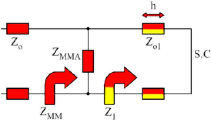
The MMA can be represented using a TL model. In this model, the straight metallic strip is represented as an inductor (), while the gap between the metallic strips is represented as a capacitor (). Additionally, the losses of the conductor and substrate, as well as any lumped resistors that may be utilized, can be modeled by a resistor (R). It is important to note that the dielectric losses increase as the number of metallic gaps increases [2]. The TL model only considers the capacitances that are aligned with the incident electric field, while disregarding those in other orientations. The specific values of inductances, capacitances, and resistors depend on the configuration and structure of the MMA unit cell and can be calculated using various mathematical formulas [2, 5, 13, 15, 16, 22, 23, 24, 25, 26]. The number of RLC resonant circuits that can be created in the TL model is determined by the number of current paths in the MMA [2]. The equivalent impedance for the ground and substrate layers is denoted by as indicated in Fig. 1.
Figure 1: TL model for the MMA.
| (5) |
Where represents the characteristic impedance of the substrate, and is the substrate thickness. () represents the propagation constant in the dielectric substrate layer, while represents the attenuation constant, and denotes the phase constant. and denote the frequency and speed of light, respectively. Also, the complex relative permeability in the substrate is denoted as , and the complex relative permittivity inside the substrate is represented by (), where and represent the relative permittivity and the conductivity of the substrate, respectively. represents the permittivity of free space. The impedance of the resonant layer of the MMA () is given as:
| (6) |
The total number of RLC resonant circuits in the TL model is represented by . The input impedance of the MMA can be expressed as follows:
| (7) |
Equations (2), (3), and (4) can also be applied similarly to the TL model to determine the absorptivity of the MMA.
III. RESULTS AND DISCUSSION
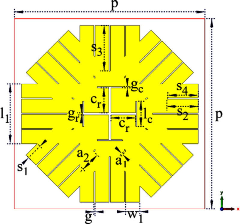
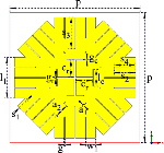
The proposed MMA unit cell consists of the top layer featuring a slotted octagonal metallic patch printed on an FR-4 dielectric substrate, backed by a grounded metallic layer. The relative permittivity of FR-4 is 4.3, with a thickness of 1.6 mm, and a loss tangent of 0.025. The FR-4 substrate was selected for the proposed MMA due to its high-loss characteristics. Both the top and bottom metallic layers are constructed from copper, each with a thickness of 0.035 mm. The octagonal shape was selected for constructing the unit cell to achieve symmetry. The dimensions of the unit cell were determined based on the desired operational frequency. Incorporating slots into the octagonal shape induces resonances at the desired frequency bands. By selecting the octagonal shape for the unit cell, optimizing its geometry, and utilizing slots within the octagonal shape, it is possible to control the values of permittivity and permeability of the MMA unit cell, thereby improving the absorption properties of the MMA. The proposed unit cell size is 28.854 mm 28.854 mm; the dimension parameters are shown in Fig. 2.
Figure 2: Geometry of the proposed MMA unit cell. ( = 28.854 mm, = 2.426 mm, = 4.734 mm, = 6.963 mm, = 4.574 mm, = 2.148 mm, = 0.16 mm, = 0.226 mm, = 3.038 mm, = 9.073 mm, = 3.833 mm, = 3.76 mm, = 0.325 mm, = 0.175 mm).
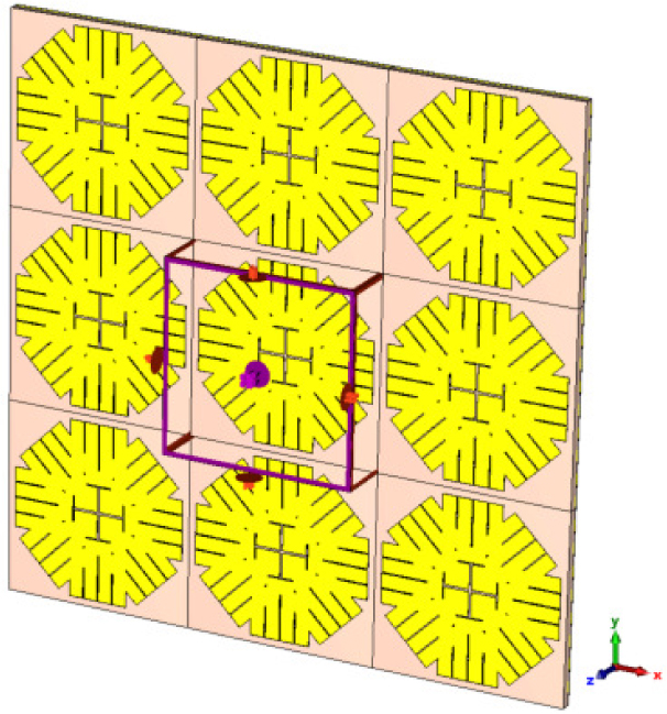
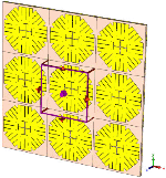
The absorptivity of the proposed MMA was simulated using the S-parameters obtained from the frequency domain solver in CST MWS. In the frequency domain solver, the periodic boundary conditions and Floquet port excitation were adopted to approximate the periodic structure of the MMA as shown in Fig. 3. The proposed MMA unit cell was excited with two Floquet modes: TE and TM. In the TE mode, the incident wave propagates in the z-direction, with the electric field polarized in the y-direction, while the magnetic field is directed in the x-direction. On the other hand, in the case of the TM mode, the incident wave also propagates in the z-direction, with the electric field polarized in the x-direction and the magnetic field in the y-direction.
Figure 3: CST simulation for the proposed MMA using frequency domain solver.
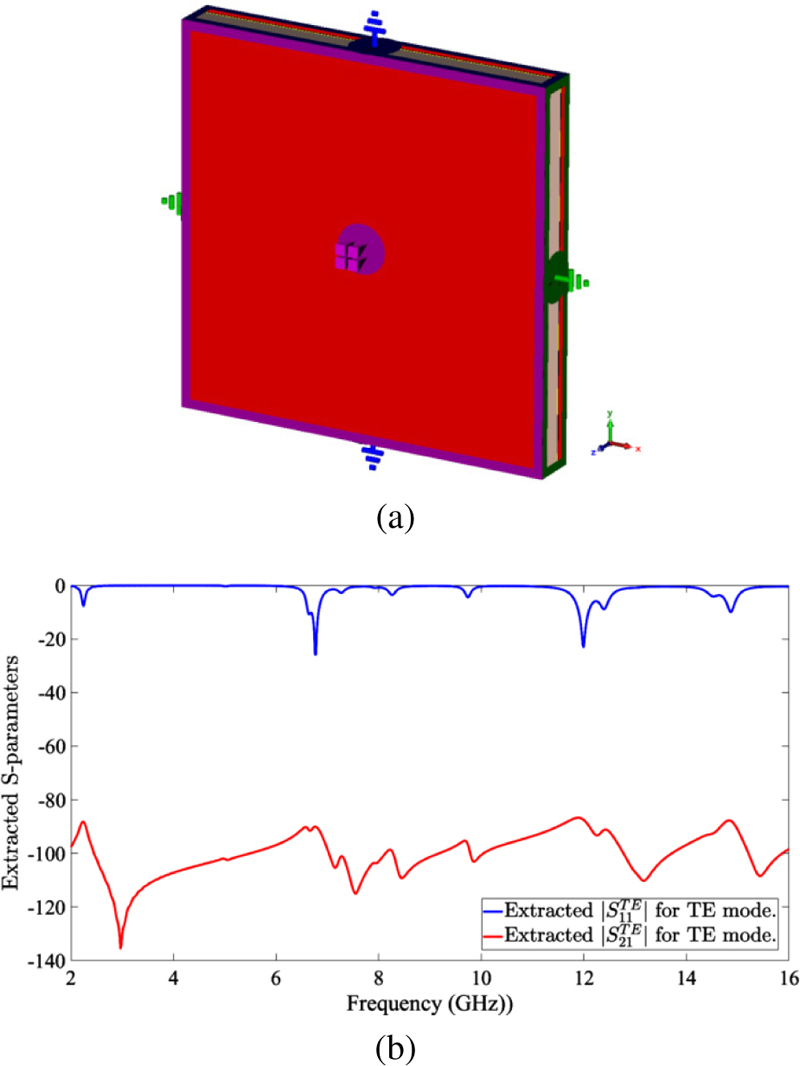
To extract the material properties of the proposed MMA, a time domain solver with two TE ports is used in CST simulation to obtain the reflection coefficient () and transmission coefficient (), as illustrated in Fig. 4. Here, defines the reflection coefficient when the reflected and incident waves are at port 1, while represents the transmission coefficient for reflected and incident waves at ports 2 and 1, respectively. The permeability, permittivity, refractive index, and normalized impedance of the proposed MMA have been simulated using MATLAB. The MATLAB simulations utilized the extracted S-parameters obtained from the time domain solver in CST, with mathematical formulations provided in [27].
Figure 4: CST model with two TE ports to extract the S-parameters of the proposed MMA unit cell: (a) CST model and (b) extracted S-parameters.
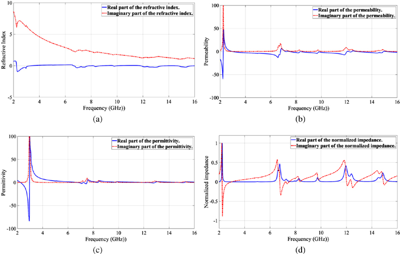
The real part of the refractive index exhibits negative values around the resonance frequencies of 2.245 GHz, 6.76 GHz, 12 GHz, and 14.88 GHz, demonstrating the metamaterial properties of the proposed absorber, as illustrated in Fig. 5. Moreover, the imaginary part of the permeability has higher values near the resonance frequencies as shown in Fig. 5. Furthermore, the value of the imaginary part of the permittivity increases in the vicinity of the resonance frequencies, as shown in Fig. 5. The proposed MMA unit cell will be matched at frequencies of 2.245 GHz, 6.76 GHz, 12 GHz, and 14.88 GHz. This occurs when the real part of the normalized impedance tends to have high values, while the imaginary part is close to 0, as illustrated inFig. 5.
Figure 5: MATLAB simulation for the material properties of the proposed MMA unit cell: (a) refractive index, (b) permeability, (c) permittivity, and (d) normalized impedance.
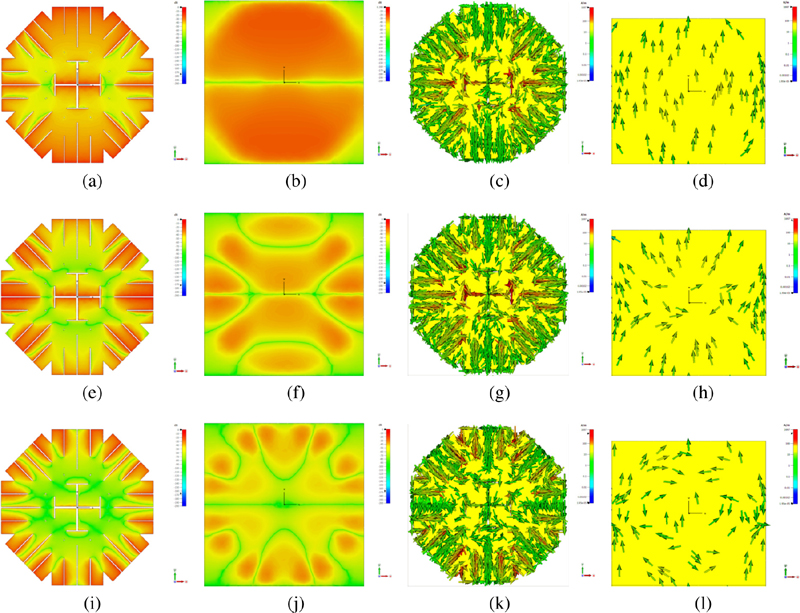
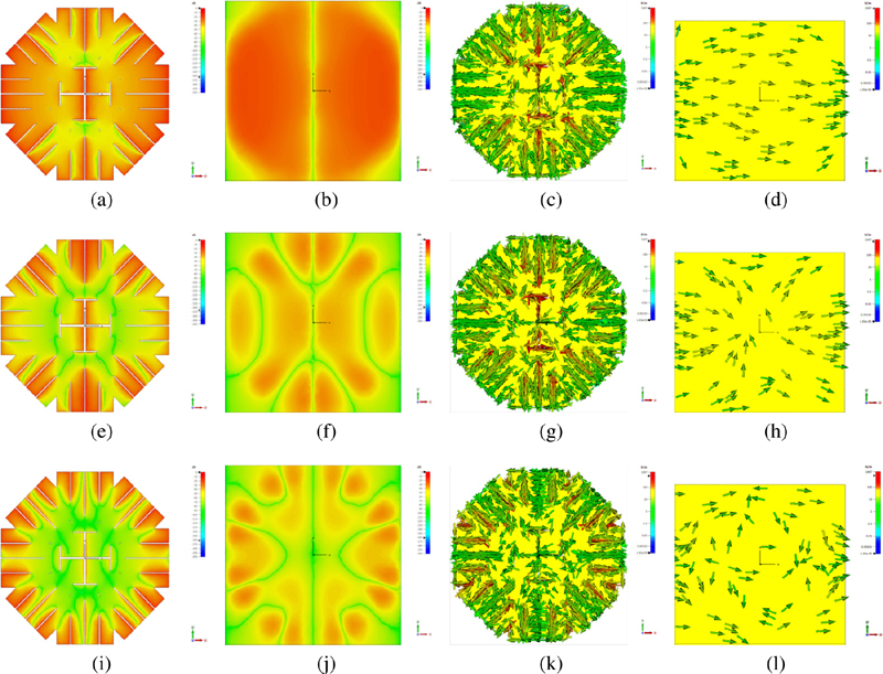
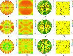
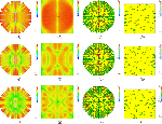
The electric field and surface current distributions for the proposed MMA were simulated using CST at 2.35 GHz, 6.97 GHz, and 11.87 GHz under TE and TM wave excitations to analyze the absorption mechanism in the proposed MMA unit cell. In TE mode excitation, the electric field on the top layer is more concentrated along the y-direction. The electric field intensity decreases at the center of the MMA unit cell as the resonance frequency increases as shown in Figs. 6, 6, and 6. Additionally, on the bottom layer, the electric field concentration becomes more weakened as the resonance frequency increases, leading to a greater reduction in capacitive leakage loss as indicated in Figs. 6, 6, and 6. In the TM mode, the electric field distribution remains the same as in the TE mode, but the electric field is concentrated along the x-axis on the top and bottom layers as shown in Figs. 7, 7, 7, 7, 7, and 7. As the resonance frequency increases, there is a corresponding increase in the number of metallic gaps, which consequently leads to higher dielectric losses [2]. However, there is a greater decrease in the concentration of the electric field across a larger area on the top and bottom layers, thereby causing a reduction in capacitive leakage losses. The increase in resonance frequency results in an overall-decrease in losses and the imaginary part value of permittivity associated with electric field distribution under both TE and TM as indicated in Fig 5. In the TE mode excitation at 2.35 GHz, surface currents on the top and bottom layers flow in opposite directions, creating cyclic current loops in the y-axis direction as shown in Figs. 6 and6.
Figure 6: Electric field and surface current distributions for the proposed MMA under TE mode excitation: (a) TE mode - top layer (E-field at 2.35 GHz), (b) TE mode - bottom layer (E-field at 2.35 GHz), (c) TE mode - top layer (surface current at 2.35 GHz), (d) TE mode - bottom layer (surface current at 2.35 GHz), (e) TE mode - top layer (E-field at 6.97 GHz), (f) TE mode - bottom layer (E-field at 6.97 GHz), (g) TE mode - top layer (surface current at 6.97 GHz), (h) TE mode - bottom layer (surface current at 6.97 GHz), (i) TE mode - top layer (E-field at 11.87 GHz), (j) TE mode - bottom layer (E-field at 11.87 GHz), (k) TE mode - top layer (surface current at 11.87 GHz), and (l) TE mode - bottom layer (surface current at 11.87 GHz).
This leads to high permeability due to magnetic resonances along the y-axis. With increasing resonance frequency, these current loops gradually shift away from the y-axis and begin to flow in multiple directions, as depicted in Figs. 6, 6, 6, and 6, leading to reduced magnetic resonances and a decrease in the imaginary part value of permeability as shown in Fig. 5. Similarly, in the TM mode, cyclic current loops are formed in the x-axis direction, with the imaginary part value of permeability decreasing as the resonance frequency increases as illustrated in Figs. 7, 7, 7, 7, 7, and 7.
Figure 7: Electric field and surface current distributions for the proposed MMA under TM mode excitation: (a) TM mode - top layer (E-field at 2.35 GHz), (b) TM mode - bottom layer (E-field at 2.35 GHz), (c) TM mode - top layer (surface current at 2.35 GHz), (d) TM mode - bottom layer (surface current at 2.35 GHz), (e) TM mode - top layer (E-field at 6.97 GHz), (f) TM mode - bottom layer (E-field at 6.97 GHz), (g) TM mode - top layer (surface current at 6.97 GHz), (h) TM mode - bottom layer (surface current at 6.97 GHz), (i) TM mode - top layer (E-field at 11.87 GHz), (j) TM mode - bottom layer (E-field at 11.87 GHz), (k) TM mode - top layer (surface current at 11.87 GHz), and (l) TM mode - bottom layer (surface current at 11.87 GHz).
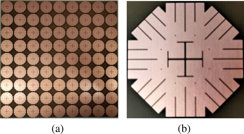
Figure 8: Fabricated prototype of the proposed MMA: (a) 9 9 unit cells and (b) enlarged unit cell.
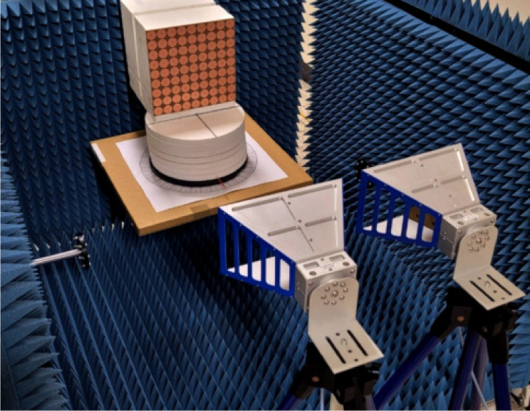
Figure 9: Experimental setup for the proposed MMA.
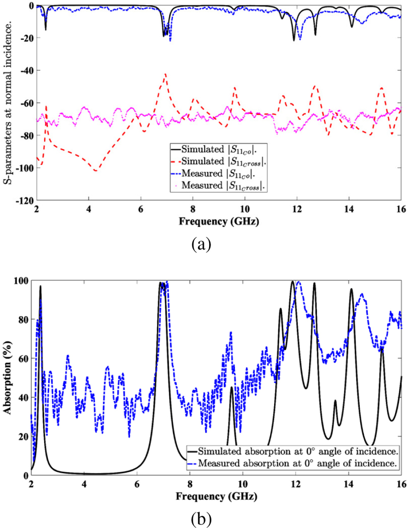
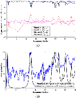
Figure 8 shows the fabricated prototype of the proposed MMA consisting of 9 9 unit cells. The experimental setup for the proposed MMA is shown in Fig. 9. The experimental setup utilizes a pair of double-ridged waveguide horn antennas operating in the frequency band of 0.8–18 GHz. The S-parameters were measured using a Rohde Schwartz ZNB 40 vector network analyzer. Initially, the S-parameters of a metallic sheet were measured as a reference. Subsequently, the metallic sheet was replaced with the fabricated prototype, and the S-parameters were remeasured and normalized. The S-parameter corresponding to the reflection coefficient with the reflected and transmitted waves in TE mode () is used to determine the perpendicular polarization reflection coefficient as . Furthermore, the cross S-parameter representing the reflection coefficient with the reflected wave in the TE mode and the incident wave in the TM mode is used to calculate the reflection coefficient for parallel polarization as . In order to measure the parameter, the alignment of the transmitting and receiving horn antennas is crucial, with both antennas being oriented vertically and parallel to the y-axis as indicated in Fig. 9. Furthermore, the transmitting horn antenna will be horizontally positioned, while the receiving antenna will be vertically positioned to measure the parameter. The simulated and measured magnitudes of the S-parameters and are depicted inFig. 10.
Figure 10: Simulated and measured S-parameters and absorption at normal incidence for the proposed MMA: (a) simulated and measured magnitudes of the S-parameters at normal incidence and (b) simulated and measured absorption at normal incidence.
Absorptivity, also known as absorption, refers to the ability of a designed structure to absorb electromagnetic radiation that is incident upon it within a specific frequency range. For the proposed MMA, the absorption can be expressed as: . Figure 10 shows the simulated and measured absorption at normal incidence for the proposed MMA. The measured results indicate that across the frequency bands of 2.22–2.38 GHz, 6.86–7.24 GHz, 11.68–12.71 GHz, 14.1–14.8 GHz, and 15.47–16 GHz, the measured absorption exceeds 75%, indicating the multiple-band absorption characteristics for the proposed MMA.
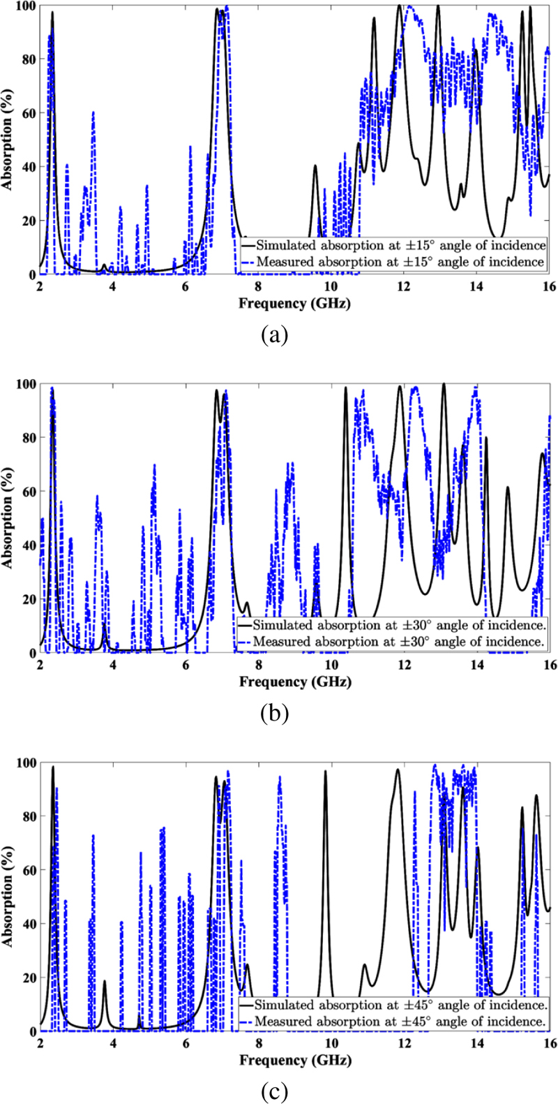
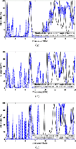
Although the decrease in losses is observed within the proposed MMA structure at higher resonance frequencies, the proposed MMA exhibits higher measured absorption in the frequency ranges of 6.86–7.24 GHz and 11.68–12.71 GHz due to better matching and lower values of the reflection coefficient (). The absorption characteristics of the proposed MMA depend on the incident angle. At angle of incidence, the frequency bands exhibiting absorption exceeding 75% are almost the same as those observed under normal incidence, as shown in Fig. 11. Conversely, when the incident angle is increased to , the frequency bands with absorption rates exceeding 75% will shift to be 2.29–2.41GHz, 6.9–6.95 GHz, 7.05–7.21 GHz, 10.6–11.14 GHz, 12.09–12.6 GHz, 13.71–14.09 GHz, and 15.96–16 GHz as indicated in Fig. 11. Additionally, the frequency bands with absorption rates higher than 75% vary as the angle of incidence increases, as indicated in Fig. 11.
The variations observed between the simulated and measured results can mainly be attributed to the small size of the fabricated sample. The proposed MMA can be valuable in a wide range of practical applications across various fields. This is particularly relevant in situations where normal or near-normal incidence is prevalent, and where efficient absorption is crucial. The developed MMA could be utilized in the future for wireless energy harvesting applications.
Figure 11: Simulated and measured absorption at oblique incidence for the proposed MMA: (a) simulated and measured absorption at angle of incidence, (b) simulated and measured absorption at angle of incidence, and (c) simulated and measured absorption at angle of incidence.
Table 1: Comparison of the proposed MMA with recently published studies on metamaterial absorbers
| Ref | Structure | Unit Cell Size | Thickness | Center Freq. (GHz) | Absorption Bandwidth (at -3 dB) | PI |
| [2] | An FSS hexagonal unit cell based on an inter-digital capacitor pattern. | 0.49 0.49 | 0.058 | 9.61 10.35 |
10% 10% |
yes |
| [4] | Two resonators printed on the upper surface of dual side copper coated Fr-4 epoxy glass substrate. | 0.11 0.11 | 0.011 | 4.195 9.345 11.48 |
4% 3.75% 4.12% |
yes |
| [5] | Modified segmented split-ring-based symmetric metamaterial. | 0.34 0.34 | 0.059 | 11.23 14.18 17.37 19.18 |
1.74% 2.92% 2.8% 3.7% |
yes |
| [9] | An octagonal ring, cross-wires, and cut-off circle artificial structure. | 0.423 0.423 | 0.031 | 12.2 | 0.05% | yes |
| [25] | Two split rings and two arms with outer square split-ring resonator. | 0.08 0.08 | 0.013 | 2.5 4.9 6 |
3.2% 3.54% 3.57% |
no |
| [26] | Modified square split ring resonator structure with a cross-strip line. | 0.44 0.44 | 0.088 | 4.62 16.3 |
2.5% 2.7% |
yes |
| [28] | Four groups of dipoles lying around a metallic ring connected by four groups of pins. | 0.12 0.12 | 0.022 | 3.25 9.45 10.9 |
5.6% 4.3% 4.6% |
yes |
| [29] | Top of the unit cell consists of eight circular sector. | 0.31 0.31 | 0.025 | 9.26 | 5.5% | yes |
| [30] | Metallic split ring resonators surrounded by E-shaped fractals. | 1.73 1.73 | 0.08 | 24 | 33.3% | yes |
| [31] | MMA unit cell with three elongated patch resonators of identical size and shape. | 0.82 0.82 | 0.068 | 16.919 21.084 25.266 |
4.73% 2.37% 3.96% |
yes |
| This work | MMA unit cell features a symmetrical structure with a slotted octagonal metallic patch. | 0.21 0.21 | 0.001 | 2.3 7.05 12.19 14.45 15.73 |
6.96% 5.39% 8.45% 4.84% 3.37% |
yes |
Table 1 presents a comparison between the proposed MMA and the previously published works on MMA. The proposed MMA offers a simple symmetrical structure characterized by a compact size, low profile, and insensitivity to polarization. Moreover, the proposed MMA exhibits a greater number of absorption bands compared to previous studies published on MMA.
IV. CONCLUSION
In this study, a new design has been proposed to achieve a compact, thin, polarization-insensitive, and multiple-band MMA using an FR4 substrate without resistive lumped elements. The proposed MMA features a symmetrical structure with a slotted octagonal metallic patch printed on an FR4 dielectric substrate, backed by a grounded metallic layer. Furthermore, the simulations and experimental results indicate that the proposed MMA can efficiently absorb incident waves. The proposed MMA can provide five absorption bands with measured absorptivity exceeding 75%. The developed absorber structure has the potential for use in various wireless communication and defenseapplications.
ACKNOWLEDGMENT
This work was supported in part by the Korean Government (MSIT) through the National Research Foundation of Korea, South Korea, under Grant 2019R1C1C1008102 and in part by the Institute of Information & Communications Technology Planning & Evaluation (IITP) grant funded by the Korea government (MSIT), under Grant RS-2022-00156409 (ICT innovation human resources 4.0).
REFERENCES
[1] I. Catalkaya and S. Kent, “An optimized microwave absorber geometry based on wedge absorber,” Applied Computational Electromagnetics Society (ACES) Journal, vol. 32, no. 7, pp. 621-627, 2017.
[2] J. Lee, M. Yoo, and S. Lim, “A study of ultra-thin single layer frequency selective surface microwave absorbers with three different bandwidths using double resonance,” IEEE Transactions on Antennas and Propagation, vol. 63, no. 1, pp. 221-230, 2014.
[3] F. Erkmen, T. S. Almoneef, and O. M. Ramahi, “Scalable electromagnetic energy harvesting using frequency-selective surfaces,” IEEE Transactions on Microwave Theory and Techniques, vol. 66, no. 5, pp. 2433-2441, 2018.
[4] N. Mishra, D. K. Choudhary, R. Chowdhury, K. Kumari, and R. K. Chaudhary, “An investigation on compact ultra-thin triple band polarization independent metamaterial absorber for microwave frequency applications,” IEEE Access, vol. 5, pp. 4370-4376, 2017.
[5] S. Hannan, M. T. Islam, N. M. Sahar, K. Mat, M. E. Chowdhury, and H. Rmili, “Modified-segmented split-ring based polarization and angle-insensitive multi-band metamaterial absorber for X, Ku and K band applications,” IEEE Access, vol. 8, pp. 144051-144063, 2020.
[6] K. Lee and S. K. Hong, “Rectifying metasurface with high efficiency at low power for 2.45 GHz band,” IEEE Antennas and Wireless Propagation Letters, vol. 19, no. 12, pp. 2216-2220, 2020.
[7] W. Xin, Z. Binzhen, W. Wanjun, W. Junlin, and D. Junping, ‘‘Design and characterization of an ultrabroadband metamaterial microwave absorber,” IEEE Photonics Journal, vol. 9, no. 3, pp. 1-13, 2017.
[8] Y. Wei, J. Duan, H. Jing, Z. Lyu, J. Hao, Z. Qu, J. Wang, and B. Zhang, “A multiband, polarization-controlled metasurface absorber for electromagnetic energy harvesting and wireless power transfer,” IEEE Transactions on Microwave Theory and Techniques, vol. 70, no. 5, pp. 2861-2871, 2022.
[9] M. J. Uddin, M. H. Ullah, and S. Z. Islam, “A broadband polarized metamaterial absorber driven by strong insensitivity and proximity effects,” IEEE Access, vol. 9, pp. 131672-131684, 2021.
[10] M. D. Banadaki, A. A. Heidari, and M. Nakhkash, “A metamaterial absorber with a new compact unit cell,” IEEE Antennas and Wireless Propagation Letters, vol. 17, no. 2, pp. 205-208, 2017.
[11] F. Erkmen and O. M. Ramahi, “A scalable, dual-band absorber surface for electromagnetic energy harvesting and wireless power transfer,” IEEE Transactions on Antennas and Propagation, vol. 69, no. 10, pp. 6982-6987, 2021.
[12] D. Kundu, S. Baghel, A. Mohan, and A. Chakrabarty, “Design and analysis of printed lossy capacitive surface-based ultrawideband low-profile absorber,” IEEE Transactions on Antennas and Propagation, vol. 67, no. 5, pp. 3533-3538, 2019.
[13] M. Hossain, N. Nguyen-Trong, K. Sayidmarie, and A. Abbosh, “Equivalent circuit design method for wideband nonmagnetic absorbers at low microwave frequencies,” IEEE Transactions on Antennas and Propagation, vol. 68, no. 12, pp. 8215-8220, 2019.
[14] S. Sambhav, J. Ghosh, and A. K. Singh, “Ultra-wideband polarization insensitive thin absorber based on resistive concentric circular rings,” IEEE Transactions on Electromagnetic Compatibility, vol. 63, no. 5, pp. 1333-1340, 2021.
[15] F. Costa, S. Genovesi, A. Monorchio, and G. Manara, “Low-cost metamaterial absorbers for sub-GHz wireless systems,” IEEE Antennas and Wireless Propagation Letters, vol. 13, pp. 27-30, 2013.
[16] M. S. Islam, M. Samsuzzaman, G. K. Beng, N. Misran, N. Amin, and M. T. Islam, “A gap coupled hexagonal split ring resonator based metamaterial for S-band and X-band microwave applications,” IEEE Access, vol. 8, pp. 68239-68253, 2020.
[17] X. Duan, X. Chen, and L. Zhou, “A metamaterial electromagnetic energy rectifying surface with high harvesting efficiency,” AIP Advances, vol. 6, no. 12, pp. 1-7, 2016.
[18] P. Zuo, T. Li, M. Wang, H. Zheng, and E.-P. Li, “Miniaturized polarization insensitive metamaterial absorber applied on EMI suppression,” IEEE Access, vol. 8, pp. 6583-6590, 2019.
[19] M. M. Zargar, A. Rajput, K. Saurav, and S. K. Koul, “Single-layered flexible dual transmissive rasorbers with dual/triple absorption bands for conformal applications,” IEEE Access, vol. 9, pp. 150426-150442, 2021.
[20] M. A. Shukoor and S. Dey, “Novel dual-mode polarization insensitive wide angular stable circular ring based deca-band absorber for RCS and EMI shielding applications,” IEEE Transactions on Electromagnetic Compatibility, vol. 64, no. 5, pp. 1337-1345, 2022.
[21] T. Liu, X. Cao, J. Gao, Q. Zheng, W. Li, and H. Yang, “RCS reduction of waveguide slot antenna with metamaterial absorber,” IEEE Transactions on Antennas and Propagation, vol. 61, no. 3, pp. 1479-1484, 2012.
[22] A. F. Almutairi, M. S. Islam, M. Samsuzzaman, M. T. Islam, N. Misran, and M. T. Islam, “A complementary split ring resonator based metamaterial with effective medium ratio for C-band microwave applications,” Results in Physics, vol. 15, pp. 1-10, 2019.
[23] U. Farooq, A. Iftikhar, M. F. Shafique, M. S. Khan, A. Fida, M. J. Mughal, and D. E. Anagnostou, “C-band and X-band switchable frequency-selective surface,” Electronics, vol. 10, no. 4, pp. 1-15, 2021.
[24] S. Dey and S. Dey, “Conformal multifunction FSS with enhanced capacitance loading for high angle stable stopband filtering and microwave absorption,” IEEE Transactions on Electromagnetic Compatibility, vol. 64, no. 2, pp. 315-326, 2022.
[25] M. L. Hakim, M. T. Islam, T. Alam, S. K. Abdul Rahim, B. Bais, M. S. Islam, and M. S. Soliman, “Triple-band square split-ring resonator metamaterial absorber design with high effective medium ratio for 5G sub-6 GHz applications,” Nanomaterials, vol. 13, no. 2, pp. 1-15, 2023.
[26] M. L. Hakim, T. Alam, M. S. Soliman, N. M. Sahar, M. H. Baharuddin, S. H. Almalki, and M. T. Islam, “Polarization insensitive symmetrical structured double negative (DNG) metamaterial absorber for Ku-band sensing applications,” Scientific Reports, vol. 12, no. 1, pp. 479-497, 2022.
[27] Z. Szabó, G.-H. Park, R. Hedge, and E.-P. Li, “A unique extraction of metamaterial parameters based on Kramers–Kronig relationship,” IEEE Transactions on Microwave Theory and Techniques, vol. 58, no. 10, pp. 2646-2653, 2010.
[28] H. Zhai, C. Zhan, Z. Li, and C. Liang, “A triple-band ultrathin metamaterial absorber with wide-angle and polarization stability,” IEEE Antennas and Wireless Propagation Letters, vol. 14, pp. 241-244, 2014.
[29] T. T. Nguyen and S. Lim, “Wide incidence angle-insensitive metamaterial absorber for both TE and TM polarization using eight-circular-sector,” Scientific Reports, vol. 7, no. 1, pp. 3204-3215,2017.
[30] R. M. H. Bilal, M. A. Baqir, P. K. Choudhury, M. Karaaslan, M. M. Ali, O. Altłntas, A. A. Rahim, E. Unal, and C. Sabah, “Wideband microwave absorber comprising metallic split-ring resonators surrounded with E-shaped fractal metamaterial,” IEEE Access, vol. 9, pp. 5670-5677, 2021.
[31] H. Wu, S. Ji, J. Zhao, Z. Luo, and H. Dai, “Design and analysis of a triple-band non-zonal polarization electromagnetic metamaterial absorber,” Applied Computational Electromagnetics Society (ACES) Journal, vol. 36, no. 6, pp. 697-706, 2021.
BIOGRAPHIES

Mohamed Elhefnawy received B.S. and M.S. Degrees in Electronics and Communications Engineering from Tanta University and the Arab Academy for Science & Technology, Egypt, in 1999 and 2005, respectively. He received a Ph.D. degree in Communications Engineering from USM University, Malaysia, in 2010. Since 2023, he has been working as a senior researcher in the Department of Electronic Engineering at Gyeongsang National University (GNU) in Jinju, South Korea. He is currently on leave from the Department of Electrical Engineering at the Faculty of Engineering, October 6 University, Egypt. He has a strong academic background that includes electromagnetic field theory, wave propagation, antenna theory, and RF/Microwave engineering. His research interests include the design and development of antennas and RF/microwave components.

Kyoung Hun Kim received B.S. Degree in Electronics Engineering from Gyeongsang National University (GNU), Jinju, South Korea, in 2023. He is currently an M.S. student in the Department of Electronic Engineering at Gyeongsang National University (GNU) in Jinju, South Korea. His research interests include antenna design and the development of wireless power transfer systems.

Tae-Hyeon Kim received B.S. Degree in Electronics Engineering from Gyeongsang National University (GNU), Jinju, South Korea, in 2023. He is currently an M.S. student in the Department of Electronic Engineering at Gyeongsang National University (GNU) in Jinju, South Korea. His research interests include the design and development of antennas and measurement and improve electrical performance of aircraft radome.

Wang-Sang Lee received the B.S. degree from Soongsil University, Seoul, South Korea, in 2004, and the M.S. and Ph.D. degrees in electrical engineering from the Korea Advanced Institute of Science and Technology (KAIST), Daejeon, South Korea, in 2006 and 2013, respectively. From 2006 to 2010, he was with the Electromagnetic Compatibility Technology Center, Digital Industry Division, Korea Testing Laboratory (KTL), Ansan-si, South Korea, where he was involved in the international standardization for radio frequency identification (RFID) and photovoltaic systems as well as electromagnetic interference (EMI)/EMC analysis, modeling, and measurements for information technology devices. In 2013, he joined the Korea Railroad Research Institute (KRRI), Uiwang-si, South Korea, as a Senior Researcher, where he was involved in the position detection for high-speed railroad systems and microwave heating for low-vibration rapid tunnel excavation systems. Since 2014, he has been a Professor with the Department of Electronic Engineering, Gyeongsang National University (GNU), Jinju, South Korea. From 2018 to 2019, he was a Visiting Scholar with the ATHENA Group, Georgia Institute of Technology, Atlanta, GA, USA. His current research interests include near- and far-field wireless power and data communications systems, RF/microwave antenna, circuit, and system design, RFID/Internet of Things (IoT) sensors, and EMI/EMC. Dr. Lee is a member of IEC/ISO JTC1/SC31, KIEES, IEIE, and KSR. He was a recipient of the Best Paper Award at IEEE RFID in 2013, the Kim Choong-Ki Award Electrical Engineering Top Research Achievement Award at the Department of Electrical Engineering, KAIST, in 2013, the Best Ph.D. Dissertation Award at the Department of Electrical Engineering, KAIST, in 2014, the Young Researcher Award at KIEES in 2017, and the Best Paper Awards at IEIE in 2018 and KICS in 2019.
ACES JOURNAL, Vol. 39, No. 5, 440–451
doi: 10.13052/2024.ACES.J.390508
© 2024 River Publishers
