A Tunable Broadband Absorber Based on Active Frequency Selective Surface
Bingmei Zhang, Xianglin Kong, Ruofeng Xu, Lei Zhao, Hang Song, Shengjun Zhang, and Jiaqi Liu
1School of Information and Control Engineering
China University of Mining and Technology, Xuzhou 221116, China
bmzhangmax@163.com, xlkong@cumt.edu.cn, xuruofeng@cumt.edu.cn, leizhao@cumt.edu.cn
2Test Physics & Numerical Mathematical,
National Key Laboratory of Science and Technology, Beijing, China
songhang0412@163.com, zhangsj98@sina.com, ljq006@vip.sina.com
Submitted On: March 29, 2024; Accepted On: September 13, 2024
ABSTRACT
In this paper, a tunable metamaterial absorber (MMA) based on active frequency selective surface (FSS) is proposed, which can dynamically tune three absorption bands. The equivalent circuit model (ECM) was used to design the MMA and elucidate its mechanism of switchable absorption. By changing the state of the PIN diode in the lossy layer and FSS layer, the absorption frequency can be tuned continuously. The tuning of the three absorption bands from S- to C-band is achieved. The numerical simulation results show that the described MMA can achieve a bandwidth of 6.2 GHz and can dynamically tune between 1.86-2.70 GHz, 2.42-5.29 GHz, and 4.16-8.10 GHz. The reflectivity is lower than -10 dB, and the fractional bandwidth reaches 125.3%. In addition, the MMA’s prototype was produced and measured. The measurement results are generally consistent with the simulation results.
Index Terms: Frequency selective surface, microwave absorber, pin diode, tunable absorber.
I. INTRODUCTION
Metamaterial absorber (MMA) is a new type of artificial electromagnetic structure [1, 2] which converts the energy of incident electromagnetic waves into other energy to achieve perfect absorption. MMA is used in a variety of applications, such as stealth systems [3], electromagnetic interference [4], and reducing radar cross section (RCS) [5, 6]. In recent years, there has been much research based on MMA. Landy firstly proposed a perfect MMA [7]. Although the advantages in thickness and absorption rate are obvious, the bandwidth still needs to be expanded. As a result, the researchers began to study methods to achieve broadband absorption and obtained fruitful results [8–10]. An ultra-wideband MMA based on the cascade of multilayer resistive films has been reported, achieving an absorption rate of over 98% between 4.9-22.6 GHz and stable performance at oblique incidence [11]. However, due to the complexity of the electromagnetic environment, the absorber with fixed frequency bands has certain limitations. Tennant and Chambers utilized dipoles loaded with PIN diodes instead of resistance films to tune the reflectivity covering the spectrum from 9 GHz to 13 GHz, providing a new idea for absorption performance [12].
A tunable MMA based on four split semi-circle resonators was proposed in [13], which tunable bandwidth covered 3.8-6.8 GHz. To enhance the controllable range, an MMA based on four-axis symmetry was introduced, which can attain a tunable bandwidth of 1.6-8.0 GHz [14]. Although the tunable bandwidth increased, the absorption rate was less than 90%. Then, an active MMA based on a circular open-loop band splice strategy was demonstrated, ensuring perfect absorption of each resonant peak and achieving bandwidth reconfigurability from 2.9 GHz to 8.12 GHz [15]. However, the complex feed network was difficult to apply. To solve this problem, a MMA based on the parasitic capacitance of the PIN diode has been designed [16]. Even though it had a great advantage in adjustable bandwidth, it was limited by the unpredictable parasitic capacitance of PIN diodes and could not be applied in practice. Therefore, designing a broadband tunable MMA is technically very challenging.
This paper designs a bandwidth-reconfigurable MMA. The absorber consists of a lossy layer and a switchable frequency selective surface (FSS) layer. The loss layer is equipped with PIN diodes, which are responsible for adjusting the impedance of the absorber to change the absorption frequency. The switchable FSS layer is loaded with PIN diodes, which control the transmission and reflection states. The absorber can achieve the continuously varying reflection coefficient below -10dB in the band of 1.86-8.10 GHz, and the thickness is only 11.5 mm.
II. DESIGN AND ANALYSIS
A. Structure of the absorber
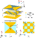
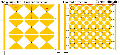
The unit structure is shown in Fig. 1. The lossy layer is designed with two opposite irregular hexagons in which a PIN diode NXP BAP 70-03 [17] is inserted into the gap. The switchable FSS layer consists of four 90 crossed slotted metal strips in an array arrangement, where a PIN diode SMP1340-079LF [18] is inserted at the split of each cross-metal strip. There is also a metal ground at the bottom of the MMA. The metallic portion of the lossy layer and switchable FSS layer are composed of copper and printed in periodic arrangement on the Rogers 5880 with thickness of d and d (relative permittivity of 2.2, dielectric loss of 0.0009), respectively. Each layer is separated by a polymethacrylimide (PMI) foam with thickness of h and h. The period of the unit cell is p. The parameters are (mm): d d 0.254, h h5.5, p19.5, b2.7, a1.5, t1.5, w0.5, v18, s3.2, m2.4, g1.2.
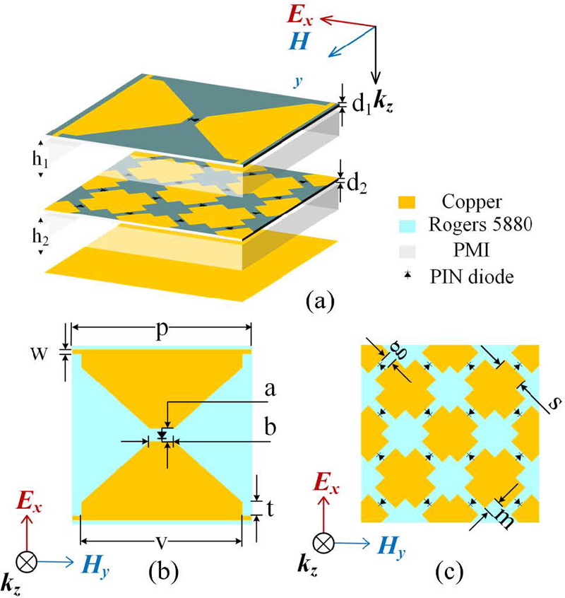
Figure 1: Structure of the design: (a) the primary structure of the proposed MMA, (b) the primary structure of the lossy layer, and (c) the primary structure of the switchable FSS layer.
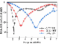
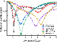
CST Microwave Studio was adopted to simulate the electromagnetic response of MMA. The reflection coefficient was obtained by simulation as shown in Fig. 2. Three different states cover the frequency band of 1.86-8.10 GHz. The lossy layer is equivalent to two dipoles with a quarter-wavelength. Depending on the resistance and current characteristics of the PIN diodes, their resistance can be controlled by the forward current of the external bias voltage. The resistance shown is the equivalent resistance of the active device of the lossy layer at different currents. The on-state and off-state of the PIN diode in the switchable FSS layer are denoted by ON and OFF, respectively. The PIN diodes loaded on the switchable FSS layer are treated as radio frequency (RF) switches, which are equivalent to small resistors and inductors in the on-state. However, they are equivalent to large resistors and capacitors in the off-state. The simulation results show that the reflection coefficient of the MMA is changed by adjusting the equivalent resistance of the lossy layer and the state of the switchable FSS layer. When the PIN diodes of the switchable FSS layer are in the off-state, the equivalent resistance of the lossy layer is 75 , and the reflection coefficient is lower than -10 dB in the frequency band of 1.86-2.77 GHz. Simultaneously, the equivalent resistance of the lossy layer is adjusted to 175 , and the reflection coefficient is less than -10dB in the frequency band from 2.43 GHz to 5.20 GHz. In order to produce absorption effects in the frequency band of 4.14-8.10 GHz, the PIN diodes of the switching FSS layer are in the on-state, and the equivalent resistance of the lossy layer is 200.
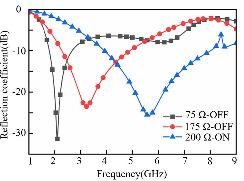
Figure 2: Reflection coefficient of the MMA calculated from CST for normal incidence.
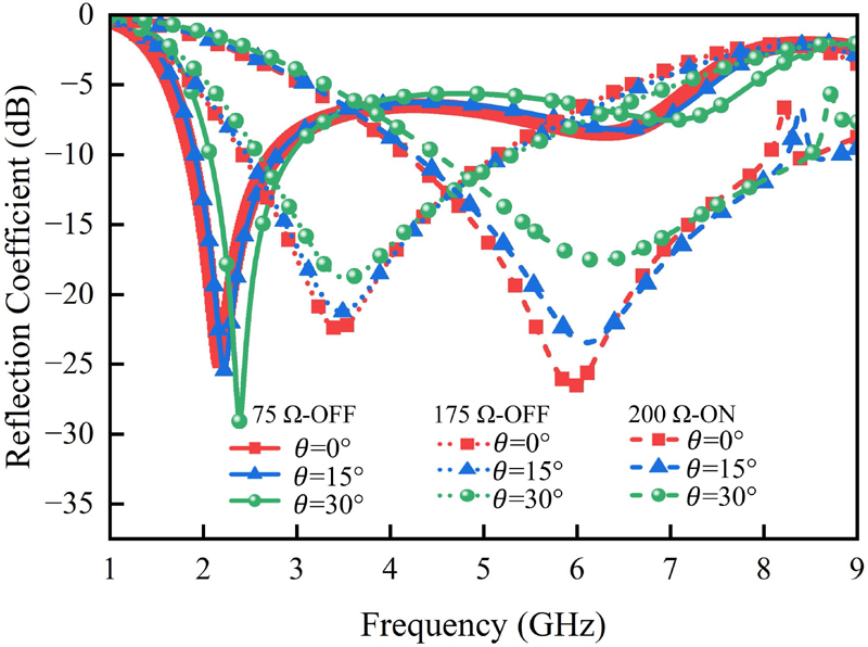
Figure 3: Simulated reflectivity at different oblique incidence
When the PIN diode is in the on-state, the switchable FSS layer presents a reflective plane. Based on the metal shielding characteristics, incident electromagnetic waves cannot penetrate this layer, and the effective thickness of the MMA is h. When the PIN diodes are in the off-state, the incoming electromagnetic wave passes the switchable FSS layer to reach the metal ground, and the effective thickness of the MMA is h+h. Therefore, the effective thickness of MMA can be changed by adjusting the state of the PIN diodes on the switchable FSS layer, which enables switching between different frequency bands. Under oblique incidence , the reflection coefficient of the MMA is shown in Fig. 3. MMA has little effect on performance between 0 and 30.
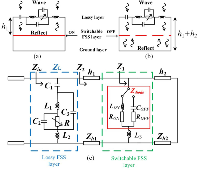
Figure 4: ECM of the proposed wideband reconfigurable MMA.
B. Equivalent circuit of the absorber
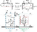
Figure 4 shows the equivalent circuit model (ECM) of this MMA. The ECM of MMA consists of two parts, including the lossy layer circuit and the switchable FSS layer circuit. The equivalent circuit structure of the lossy FSS layer includes C, C, C, L, L, and R. C is the capacitance effect generated by the gap between the units in the lossy layer. The gap capacitance between the hypotenuse sides of the hexagonal in the lossy layer is regarded as C. C is the gap capacitance in the middle gap of the lossy layer. L and L both represent the equivalent inductance of the hexagonal to the lossy layer. The equivalent circuit of the switchable FSS layer includes L and Z. L is the equivalent inductance of the metal strip on the switchable FSS layer. Z has two states, including the on-state and the off-state. The substrate is equivalent to lossy transmission line models, where the substrate thickness is represented by h and h, and their characteristic impedances are represented by Z and Z, respectively. In this paper, the absorption rate is improved by reducing the reflectivity. When the input impedance Z of the MMA matches the free space impedance Z, the reflectivity of the MMA is diminished.
The input impedance of the overall MMA is:
| (1) | ||
| (2) | ||
| (3) | ||
| (4) | ||
| (5) |
where Z represents the impedance of the loss FSS later, and and are the phase constants of the substrate (Z) and the substrate (Z).
The reflection coefficient of this MMA is expressed as:
| (6) |
When the resistance is very small, it is equivalent to the PIN diode in the on-state. The PIN diode of the switching FSS layer is in the on-state, causing the gaps in the structure to connect. This layer acts as an ideal reflector, and the equivalent thickness of the MMA is shortened to h At this point, if the equivalent resistance of the PIN diode in the lossy layer is adjusted to 200 , this MMA produces a wide absorption band at high frequency. The PIN diode is in the off-state when the equivalent resistance is large. When the switchable FSS layer’s PIN diodes are turned off, this layer is regarded as a transparent window. The thickness of the MMA increases and the absorption peak is generated in the medium frequency band. In addition, when the equivalent resistance of the lossy layer’s PIN diodes was tuned to 75 , the absorption band moved to a lower frequency. Therefore, the absorption frequency band variation of the absorber is affected by the combined action of the PIN diode in the lossy layer and the switchable FSS layer.
Comparison between the simulation results of ECM and the simulation results of CST can well verify the correctness of the equivalent circuit model. As shown in Fig. 5, the curve of the two results coincides well.
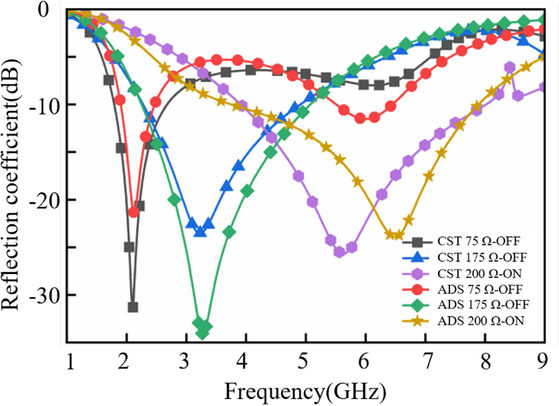
Figure 5: Reflection coefficient of MMA from CST and ECM.
C. Analysis of absorption mechanism
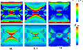
Figures 6 (a) and (b) show the vector current density and electric field distribution of resonant points at 2.1 GHz and 3.47 GHz, at which point all PIN diodes in the switchable FSS layer can be in the off-state. Figure 6 (c) shows the vector current density and electric field distribution at the resonance point of 6.0 GHz when the PIN diodes in the switchable FSS layer are in the on- state.

Figure 6: Vector current density distribution and electric field distribution of MMA: (a) f 2.1 GHz, (b) f 3.47 GHz, and (c) f 6.0 GHz.
At different resonance points, the PIN diode of the lossy layer exhibits induced current and correspondingly generates a strong electric field. This indicates that the energy of the incident wave is dissipated by the equivalent resistance of the PIN diode in the lossy layer. At 2.1 GHz and 3.47 GHz, the electric field is distributed on the conductive metal of the lossy layer and the switchable FSS layer. The current is distributed across the conductive metal of the lossy layer. The difference equivalent resistance of the PIN diode in the lossy layer changes the input impedance of the MMA and thus affects the resonant frequency of the MMA. At 6.0 GHz, the electric field is distributed over the lossy layer conducting the metal, while the current flows between the lossy layer and the switchable layer. The existence of the FSS layer is equivalent to a switching ground plane, which realizes the thickness change of the MMA.
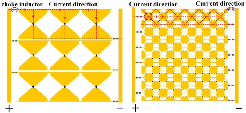
Figure 7: MMA’s vector current density and electric field origin of resonance: (a) feed network of the lossy layer and (b) feed network of the switchable layer.
III. EXPERIMENTAL VERIFICATION
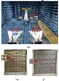
The DC bias feed network of the MMA is shown in Fig. 7. The lossy layer’s feed network arrangement is shown in Fig. 7 (a), which has paths that allow DC flow. Figure 7 (b) shows a switchable FSS layer feed network arrangement. The switchable FSS layer separately sets multiple dedicated bias lines and connects the anode and the cathode of the PIN diode to different bias lines without affecting the absorption effect of the structure. In addition, the main reason for introducing RF chokes is to eliminate the effect of the feed network on MMA. Based on the analysis of the above simulated results, a 1313 absorber sample was fabricated using printed circuit board (PCB) technology. The overall size of the sample is 277.5 mm257.5 mm.
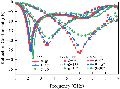
To affirm the proposed MMA, the reflection coefficient is measured by the free space method in the direct measurement method in the microwave darkroom. The measurement environment and the sample to be tested are shown in Fig. 8. Two wideband horn antennas (LB-10125-SF) working in 1-12.5 GHz [19], one for transmitting and one for receiving, are connected to the vector network analyzer via coaxial cable. During measurement, the DC voltage sources provide different bias voltages for the lossy layer and the switchable FSS layer PIN diodes. The resistance value of each PIN diode under different bias voltages is predicted by measuring the forward current value of the channel. To prevent the absorber to be measured from being damaged by excessive voltage, a resistor can be inserted into the circuit for voltage division. Figure 9 shows comparisons between simulation results and measure results. In general, the absorber has frequency reconfiguration characteristics. The simulation results are in agreement with the measured results.
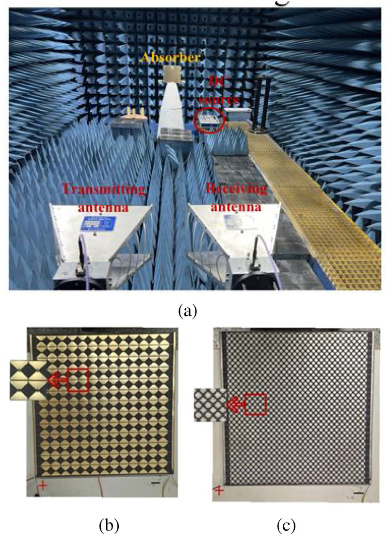
Figure 8: (a) Measurement environment of the proposed MMA, (b) the lossy layer, and (c) the switchable FSS layer.
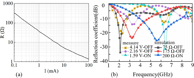
Figure 9: (a) Relationship between on-state current and resistance and (b) comparison between simulation results and measured results.
IV. CONCLUSION
This paper proposes a wideband reconfigurable MMA for electromagnetic shielding in different bands (S, C). The MMA structure comprises a lossy layer and a switchable FSS layer. The absorption band tuning can be achieved by reasonably adjusting the PIN diode state of each layer. Under normal incident conditions, the absorber can achieve a bandwidth of 6.2 GHz and is dynamically tuned between 1.86-2.70 GHz, 2.42-5.29 GHz, and 4.16-8.10 GHz. The thickness of the MMA is only 11.5 mm, with a fractional bandwidth of 125.3%. Additionally, this design holds promising applications in electromagnetic cloaking and shielding.
ACKNOWLEDGMENT
Bingmei Zhang and Xianglin Kong contributed equally to this work. This work was supported in part by the Fundamental Research Funds for the Central Universities under Grant 2023XSCX026; in part by the Postgraduate Research & Practice Innovation Program of Jiangsu Province under KYCX23_2707; in part by the Graduate Innovation Program of China University of Mining and Technology under Grant 2023WLKXJ094; and in part by the National Natural Science Foundation of China under Grant 61771226. (Corresponding author: Lei Zhao and Jiaqi Liu.)
REFERENCES
[1] S. Narayan, J. Sreeja, V. V. Surya, B. Sangeetha, and R. U. Nair, “Radar absorbing structures using frequency selective surfaces: Trends and perspectives,” Journal of Electronic Materials, vol. 49, no. 3, pp. 1728-1741, Jan. 2020.
[2] H. Lv, Z. Yang, H. Pan, and R. Wu, “Electromagnetic absorption materials: Current progress and new frontiers,” Progress in Materials Science, vol. 127, p. 100946, June 2022.
[3] J. Wen, Q. Ren, R. Peng, and Q. Zhao, “Ultrabroadband saline-based metamaterial absorber with near theoretical absorption bandwidth limit,” IEEE Antennas and Wireless Propagation Letters, vol. 21, no. 7, pp. 1388-1392, July 2022.
[4] M. A. Shukoor and S. Dey, “Novel dual-mode polarization insensitive wide angular stable circular ring based Deca-band absorber for RCS and EMI shielding applications,” IEEE Transactions on Electromagnetic Compatibility, vol. 64, no. 5, pp. 1337-1345, Oct. 2022.
[5] S. Dey and S. Dey, “Conformal multifunction FSS with enhanced capacitance loading for high angle stable stopband filtering and microwave absorption,” IEEE Transactions on Electromagnetic Compatibility, vol. 64, no. 2, pp. 315-326, Apr. 2022.
[6] A. Dhumal, M. Bisht, A. Bhardwaj, M. Saikia, S. Malik, and K. Srivastava, “Screen printed polarization independent microwave absorber for wideband RCS reduction,” IEEE Transactions on Electromagnetic Compatibility, vol. 65, no. 1, pp. 96-103, Feb. 2023.
[7] N. I. Landy, S. Sajuyigbe, J. J. Mock, D. R. Smith, and W. J. Padilla, “Perfect metamaterial absorber,” Physical Review Letters, vol. 100, no. 20, May 2008.
[8] X. Kong, S. Zhang, X. Pang, Y. Fu, L. Zhao, and Z. Shen, “Fast design of ultra-wideband absorbers based on equivalent circuit model,” IEEE Antennas and Wireless Propagation Letters, pp. 1-5, 2024.
[9] P. Chen, X. Kong, J. Han, W. Wang, K. Han, H. Ma, L. Zhao, and X. Shen, “Wide-angle ultra-broadband metamaterial absorber with polarization-insensitive characteristics,” Chinese Physics Letters, vol. 38, no. 2, p. 027801, Feb. 2021.
[10] X. Kong, L. Zhao, F. Wang, S. Zhang, Y. Fu, X. Pang, X. Liu, and X. Shen, “A fast design method for ultra broadband absorbers using RC equivalent circuit model,” in 2022 International Applied Computational Electromagnetics Society Symposium (ACES-China), Dec. 2022.
[11] C. Liang, X. Kong, F. Wang, R. Xu, Y. Fu, X. Pang, S. Zhang, X. Shen, and L. Zhao, “A broadband perfect metamaterial absorber with angle-insensitive characteristics,” Journal of Electromagnetic Waves and Applications, vol. 37, no. 3, pp. 401-410, Feb. 2022.
[12] A. Tennant and B. Chambers, “Adaptive radar absorbing structure with PIN diode controlled active frequency selective surface,” Smart Materials and Structures, vol. 13, no. 1, pp. 122-125, Dec. 2003.
[13] S. An, H. Xu, Y. Zhang, S. Wu, J. Jiang, Y. He, and L. Miao, “Design of a polarization-insensitive wideband tunable metamaterial absorber based on split semi-circle ring resonators,” Journal of Applied Physics, vol. 122, no. 2, July 2017.
[14] H. Wang, P. Kong, W. Chen, W. Bao, X. Yu, L. Miao, and J. Jiang, “Broadband tunability of polarization-insensitive absorber based on frequency selective surface,” Scientific Reports, vol. 6, no. 1, Mar. 2016.
[15] T. Wu, W. Li, S. Chen, and J. Guan, “Wideband frequency tunable metamaterial absorber by splicing multiple tuning ranges,” Results in Physics, vol. 20, p. 103753, Jan. 2021.
[16] Z. A. P. Jibran and K. R. Jha, “Design of active tunable wide frequency covering absorber,” in 2021 International Conference on Intelligent Technologies (CONIT), June 2021.
[17] NXP Semiconductors, “BAP70-03 Silicon PIN Diode Rev. 6 – 7 March 2014,” https://www.nxp.com/docs/en/data-sheet/BAP70-03.pdf
[18] Skyworks Solutions Inc, “SMP1340 Series:Fast Switching-Speed, Low-Capacitance, Plastic-Packaged PIN Diodes,” https://www.mouser.cn/datasheet/2/472/SMP1340˙Series˙200051U-3050131.pdf
[19] Ainfoinc, “LB-10125-SF LB Specification Brochure,” https://www.ainfoinc.cn/tianxian-chanpin/laba-tianxian/kuandai-laba-tianxian/lb-10125-sf-kuandai-labatianxian-1-12-5-ghz-zengyi-11db-sma-zuo
BIOGRAPHIES

Xianglin Kong (Member, IEEE) is currently pursuing the Ph.D. degree with the China University of Mining and Technology, Xuzhou, China. His research interests include the design of RF/microwaves antennas and metasurface.

Ruofeng Xu received the B.S. (2004) degree from Suzhou University in electronics and science and technology, and the M.S. (2006) and Ph.D. (2010) degrees in electronic engineering from the University of Kent, UK. He joined the China University of Mining and Technology, Xuzhou, China, in 2011. His main interests include microwave technology and applications.

Lei Zhao (Senior Member, IEEE, Fellow, ACES), received the B.S. degree in mathematics from Jiangsu Normal University, China, in 1997, and the M.S. degree in computational mathematics and the Ph.D. degree in electromagnetic fields and microwave technology from Southeast University, Nanjing, China, in 2004 and 2007, respectively.
He joined the China University of Mining and Technology, Xuzhou, China, in 2019, where he is currently a full Professor. From August 2007 to August 2009, he worked with the department of electronic engineering, The Chinese University of Hong Kong, as a research associate. From February 2011 to April 2011, he worked with the department of electrical and computer engineering, National University of Singapore, as a research fellow. From September 2016 to September 2017, he worked with the department of electrical and computer engineering, University of Illinois at Urbana-Champaign, Champaign, IL, USA, as a visiting scholar. He has authored or coauthored more than 120 refereed journal and conference papers. His current research interests include spoof surface plasmon polaritons theory and its applications, RF/microwave antenna and filter design, computational electromagnetics, and electromagnetic radiation to human’s body.
Dr. Zhao serves as an Associate Editor for IEEE Access, an Associate Editor-in-Chief for Applied Computational Electromagnetics Society (ACES) Journal and a reviewer for multiple journals and conferences including the IEEE Trans. on Microwave Theory and Techniques, IEEE Trans. Antennas and Propagation, IEEE Antennas and Wireless Propagation Letters, ACES Journal, and other primary electromagnetics and microwave related journals.

Hang Song is a doctoral candidate at the National Key Laboratory of Experimental Physics and Computational Mathematics. He obtained his master’s degree from Beihang University. His research interests focus on target feature control technology, and he possesses specialized knowledge in the design of low-scattering characteristic metamaterials.

Shengjun Zhang received the B.Sc. degree from China University of Geosciences (Wuhan), Wuhan, China, in 1995, M.Sc. degree from China University of Geosciences (Beijing), Beijing, China, in 1998, and Ph.D. degree in Optics from Beijing University of Technology, Beijing, China, in 2001. After that, he joined National Key Laboratory of Science & Technology on Test Physics & Numerical Mathematics. He is currently the full professor of China Academy of Launch Vehicles Technology, and adjunct professor of Xi’Dian University. He is a member of space security committee of International Astronautics Federation (IAF). His research interests include electromagnetic signature simulation and control approaches, effects of cold plasma on electromagnetic waves, FSS, tuning of scattering by active array, and space security.

Jiaqi Liu was born in Yueyang, China, in 1963. He received the Ph.D. degree in circuit and systems from Beihang University, Beijing, China, in 2007. He currently serves as the Vice Director and leading Research Fellow with the National Key Laboratory of Science and Technology on Test Physics and Numerical Mathematics. His research area is signal processing and target recognition.
ACES JOURNAL, Vol. 39, No. 7, 651–657
doi: 10.13052/2024.ACES.J.390709
© 2024 River Publishers