Design of DC to 40 GHz GaAs-based MMIC Attenuators by Utilizing Full-chip Numerical Analyses
Mehmet Emin Bayrak, Harun Tekin, and Huseyin Serif Savci
Department of Electrical and Electronics Engineering
Istanbul Medipol University, Istanbul, 34810, Turkey
hsavci@medipol.edu.tr
Submitted On: March 30, 2024; Accepted On: September 1, 2024
ABSTRACT
In this study, a numerical analysis-based design methodology of monolithic microwave integrated circuit (MMIC) attenuators on a GaAs-based microwave integrated passive device (IPD) technology is presented. The designs have 0 dB, 3 dB, 4 dB, 6 dB, 10 dB, 12 dB, 20 dB, and 30 dB attenuation from DC to 40 GHz. The attenuators are designed for a maximum RF power of 26 dBm and a maximum die area of 0.25 mm. The circuits are physically compact but electrically large. The finite element method and Method of Moments (MoM)-based analyses are used. The MoM-based solutions show close correlations with the measurements. The measured return losses are better than 20 dB, and insertion loss variation is less than 0.5 dB across the entire band. This paper explains the detailed design steps and numerical electromagnetic setup to achieve first-pass success.
Index Terms: Finite element method, GaAs integrated passive device, Method of Moments, monolithic microwave integrated circuit, wideband attenuator.
I. INTRODUCTION
In recent years, millimeter wave radios entered our daily lives as integrated with several different types of consumer equipment, from 5G cellular handsets to automotive radars. These radios utilize many die products, packaged chips, or modules in their architectures. The type of architecture varies depending on the application. While high-volume products use all integrated solutions on a single die, mostly on complementary metal oxide semiconductor (CMOS) technology, the others favor combining bare dies from different technologies for several different reasons, such as design flexibility, performance, and lower development costs. The advancement of packaging technology resulted in reduced associated costs and rises in yield. Therefore, many applications utilize system-in-package (SiP) solutions where dies developed on cost-effective semiconductor processes are put together. This, coupled with the high overhead cost of the modern semiconductor process, made the system architects revisit every portion of the system for proper technology considerations. The integrated passive device (IPD) process is one of the cost-efficient solutions for passive microwave networks. The IPD can be developed on different bases such as high-resistance silicon wafers, GaAs wafers [1, 2, 3, 4, 5, 6, 7], layered ceramic substrates in either low-temperature co-fired ceramic (LTCC) [8] or high-temperature co-fired ceramic (HTCC) form [9], and several recent ones such as graphene [10, 11]. Although they essentially serve the same purpose, their electrical specs vary. The silicon and GaAs-based IPD processes are widely used for SiP solutions. Even though silicon has several times higher thermal conductivity than GaAs with less risk of local overheating under high power, the GaAs devices are more resilient to radiation exposure owing to the high proton absorption coefficient. In addition, the GaAs process allows higher voltage ratings than silicon, such as 8V, 28V, and 50V, by utilizing epitaxial layers with proper electrical properties, enabling them to be compatible with GaN power processes. GaAs IPD technologies have been used for the design of various microwave circuits.
Modern wireless communication systems, from beamformers to RF front-ends, utilize many control products, such as attenuators, switches, and phase shifters in the signal chain. They are used for conditioning the signal’s amplitude, phase, and direction through the multi-throw switches. Among all the control products, attenuators are used ubiquitously, after almost every other component in a cascaded system, for the proper amplitude adjustments of the signals. Three types of attenuators are used in RF systems; fixed, voltage-variable, and digital-step.
Fixed-value attenuators, which are also called PADs, are passive devices that provide a flat attenuation value across the specified frequency range. The fixed attenuators are classified as narrow-band (tuned), broadband, or high-power. Voltage-variable attenuators use analog DC control voltages for the attenuation level adjustment in a continuous manner [18], whereas digital step attenuators use serial or parallel control bits for discrete attenuation adjustment. Step attenuators are cascaded blocks of switchable fixed attenuators that utilize single-pole single-throw (SPST) switches to be switched in or bypassed using digital bits [16], [17]. The on-resistance and off-capacitance of these SPST switches should be considered in the design of the attenuator. These attenuators have binary-weighted attenuation values and usually take values such as 0.25, 0.5, 1, 2, 4, 8, and 16 dB [19]. The switch structures in digital attenuators can be realized using PIN diodes, MESFET, MOSFET, and pHEMT devices [20].
The building blocks of all the attenuators are resistors. However, several different topologies can be constructed with these resistors. The three significant topologies of attenuators are Tee, Pi, and Bridged-Tee topologies, as seen in Fig. 1. Although all topologies can essentially be used to obtain the desired attenuation levels, some topologies are preferred over others depending on the number and value of the resistors as well as the system requirements.
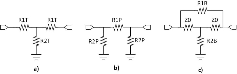
Figure 1: Attenuator topologies: (a) Tee, (b) PI, and (c) Bridged-Tee.
The value of series and shunt resistors are calculated by solving the voltages and currents using Kirchoff’s voltage and current laws. The attenuators are symmetrical and reciprocal devices allowing identical component values around the mid-symmetry line. The resistance values can be extracted using the characteristic impedance and attenuation value in dB [23], [24]. Equations (1) and (2) show the calculation of the series resistor values, R1T, and the shunt resistor value, R2T, in Tee topology. Equations (3) and (4) show the calculation of the series resistor values, R1P, and the shunt resistor value, R2P, in PI topology. Equations (5) and (6) show the calculation of the series resistor values, R1B and the shunt resistor value, R2B in Bridged-Tee topology.
| (1) | ||
| (2) | ||
| (3) | ||
| (4) | ||
| (5) | ||
| (6) | ||
| (7) |
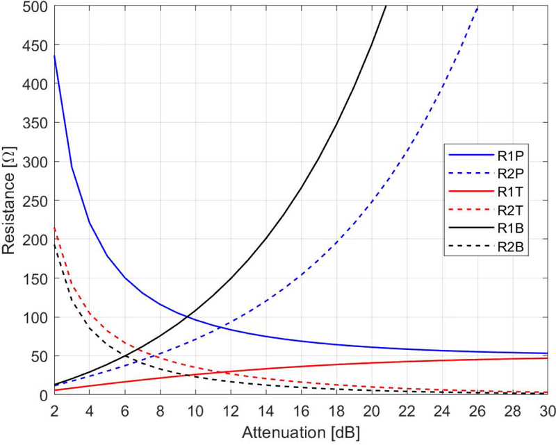
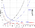
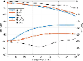
Figure 2: Resistance versus attenuation curves: blue: PI, red: Tee, black: Bridged-Tee.
These formulas are for ideal resistors without taking real resistor models and the connecting metals into account. However, resistors have parasitic capacitors and inductors dependent on their sizes, which are dictated by the resistance values and the level of current they must handle. The formulas can be updated by replacing each ideal resistor with a complex model of a real resistor. However, solving analytical equations will be error-prone as electromagnetic couplings between the structures would also affect the solutions. As an optimum solution, we analyzed the topologies to find the one with the smallest-sized resistors. The resistance values change with the attenuation levels. The IPD process used in this study has only one resistor type: thin film resistor (TFR), which has a sheet resistance of 50 per square. Considering the attenuator family would include attenuation levels from as low as 2 dB to as high as 30 dB, it would be ideal to have the lower value of resistors and not change too much with attenuation levels. It would be a prime concern to have all the designs fitting the same die area and maintaining a broadband response without introducing too much capacitance. Figure 2 shows the resistor values versus attenuation levels for the three attenuator topologies. In general, the solid lines are for the series resistance, and the dashed lines represent the shunt resistance. The blue curves are for PI-type attenuators, the red curves are for Tee-type attenuators, and the black curves are for Bridged-Tee-type attenuators. It is seen from the plots that the red curves in Fig. 2, which are for theTee-type attenuator, have lower resistance values and present the least variance over the attenuation levels. In PI topology, the value of the shunt resistor becomes as high as 790 , and in Bridged-Tee topology, the value of the series resistor is as high as 1530 . It is concluded that the Tee topology or its distributed derivative should be adopted for this study.
II. DESIGN METHODOLOGY
The attenuator family is designed using a 28V GaAs-based IPD process. The process contains three active metal layers, two capacitor options with different capacitance densities, and voltage durability. The GaAs substrate has a dielectric constant of 12.88 and roughly 0.0004 tangent loss. The die thickness is around 100 um. A half-wavelength, 50 line is 70 m wide and around 1.3 mm long at 40 GHz.
The process has only a 50 per square TFR, which is co-planar with the first metal layer. The process has two metal-insulator-metal capacitors and backvia.
All the attenuators designed in this family have broadband response between DC to 40 GHz frequency range. The circuits’ die size is as small as possible to have 0.470 mm 0.430 mm and 0.430 mm 0.570 mm, almost the minimum valid die size in this process. The attenuators can withstand up to 26 dBm of continuous RF signal power as the power levels beyond that cause excessive joule heating on the metal traces. Also, the size of resistors is adjusted to withstand up to 140C temperature values, which complies with a maximum power level of 26 dBm.
Most of today’s monolithic microwave integrated circuit (MMIC) attenuators have performance requirements such as high power handling, compact area size, and broadband operation. These requirements are contradictory. The broadband nature of the design favors small resistor sizes to reduce the associated parasitic capacitance, whereas the high input power requirements dictate larger resistors. A high-power broadband attenuator with a flat response requires a distributed design with a detailed device model and its parasitic compensation over the frequency range.
The Tee-type attenuator has two 150 m pitch Ground-Signal-Ground pads, at least two backvias for ground connection, and a minimum of three resistors. A complex equivalent circuit model for the TFR resistor and its value-limited simplified model are given in Fig. 3, where Rcore models the resistor value, Cpar models the parallel capacitor between metal connections, Csub and Rsub models shunt substrate parasitic, Lcont, and Rcont model the parasitic of metal1 to TFR connection. Although the complex model reflects a physics-based generic model for a broad range of resistance values, the simplified model also holds its validity for the range of values used in this study. The Ground-Signal-Ground pad also has a significant effect on the circuit performance with its capacitive behavior due to the large bonding plate. The backvia has an inductive behavior with roughly 0.4nH per mm.
The attenuator design starts with calculating the resistor values based on the topology and sizing it according to the required power. After the resistances are sized to cope with the rated current, their equivalent model is constructed. To compensate for the capacitive parasitic elements of the resistor and capacitance coming from the pads, low-impedance transmission lines between series resistors and high-impedance transmission lines between resistors and pads are used. The line’s rated current handling ability in those sections limits the minimum width of high-impedance lines. Sizing the width of metals below the minimum value specified in the design manual causes different failure mechanisms for different types of currents. It is electromigration failure for direct-current, whereas a joule heating failure is triggered for the RF currents. The reactive parts will be matched through these transmission lines to obtain a broadband attenuator response [21], [22]. The transmission lines are designed mainly with top metal due to their low sheet resistance, less parasitic capacitance, and higher power handling. Matching the circuits by tuning the characteristic impedance and electrical length of transmission lines is done using the equivalent schematic models. Ultra-wide-band design techniques through simplified real frequency techniques or parametric representation of Brune functions can be utilized for the desired performance [25], [26]. The desired performance should be achieved by constructing the layout within the designated area. Fitting the transmission lines, resistances, bond pads, and ground vias within such a tight area causes lots of electric and magnetic inter-couplings. Furthermore, the chip ring also causes unwanted feed, which should also be considered and embedded in the final response. The size of the die is more than a quarter wavelength at the frequency of interest, making the designs electrically large. Therefore a successful design can only be achieved with full-die electromagneticsimulations.
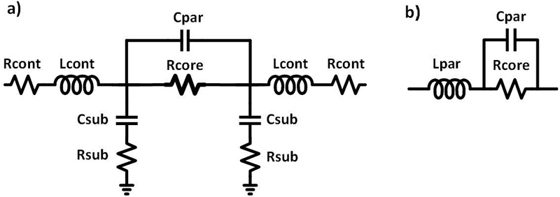
Figure 3: Equivalent circuit of the TFR: (a) complex and (b) simplified.
The broadband operation of the designs from DC to Ka-band dictates solving the complex electromagnetic interactions within the die. Keysight ADS software is used to find full-chip electromagnetic solutions utilizing FEM (Finite-Element-Method) and MoM (Method-of-Moments) numerical methods. Although commercial software guides the user to set up the simulations, the parameters such as mesh frequency, mesh density, how to mesh the vias, how to mesh the transmission line edges, method of matrix solving (direct, iterative), delta error level, order of basis function should be tailored for each structure as these would directly affect the accuracy, the convergence and the duration of analyses. The optimum settings are structure-dependent and require a good insight into the method itself [28]. For MoM simulations, an adaptive frequency plan is selected between 1 MHz and 40 GHz with a maximum of 50 points. The mesh is generated based on the highest frequency of simulation, 40 GHz. The mesh density is adjusted to have 50 cells per wavelength. The computation is done by enabling the edge mesh and transmission line mesh options, which help to improve the accuracy. The matrix is solved using the iterative dense method where the post-solvers are enabled. For FEM simulations, the same adaptive frequency plan is used. The mesh refinement is done based on the maximum frequency. The edge and vertex meshing are adjusted with 0.2 and 0.06 multiples of the estimated conductor width, respectively. As the computation stop criterion, the delta error is chosen as 0.02, along with the minimum and maximum number of adaptive passes of 2 and 15, respectively. The iterative matrix-solving method with 2nd order basis functions is used.
Besides the planar solutions, to observe the package, wire-bond, and die interactions, the dies are attached to 50 launcher through the bond wires. The wire bond effects are captured by using the 3D full-wave electromagnetic simulations of various wire and ribbon transitions based on the FEM. Keysight EmPro software is used for the 3D simulations. Wire bonding was performed with 25 μm diameter, Au-based wires, whereas 250 μm 25 μm, Au-based connections are used for ribbon bonding. Among different profiles, spline shape and JEDEC5 profile with five-defined coplanar points are used. It is verified that bond-wire length is more critical to obtaining better insertion loss than having better impedance matching [27]. The setup details and parameters of both planar and 3D numerical methods are presented throughout the paper, and the solutions are compared with the measurement results to give the reader a good insight into the setup dependency and accuracy of the solution of interest. It is shown that without correctly setting up a full-die electromagnetic numerical analysis, it is nearly impossible to achieve a first-pass success MMIC design at millimeter wave frequencies.
In the EM simulations configured with the MoM, the solution is obtained for 50 adaptive frequency points swept between DC and 40 GHz. The mesh frequency is set to 40 GHz with a mesh density of 40 cells per wavelength. The edge mesh and transmission line mesh are used for increased accuracy. The matrix is solved using the iterative dense method. The port solver is also enabled. The circular shapes in Through-Wafer-Via (TWV) are simplified with an arc resolution of 45 degrees.
A. 0 dB (THRU) design
Although considered a part of the attenuator family, THRU design is a substitute for attenuators in the system wherever no attenuation is needed. The primary target spec of the THRU design is to provide a broad matching and minimum insertion loss in the DC-40 GHz band. This circuit has the same die size and pad locations as other attenuators. The return loss value will be better than 27 dB.
Figure 4 provides an equivalent design schematic for the THRU circuit. The circuit has a single transmission line designed as a symmetrical structure. The maximum value of the line impedance is limited by the minimum metal width that can handle the current for the 26 dBm power requirement. The 0 dB attenuator layout is seen in Fig. 10 (a).
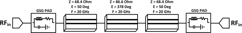
Figure 4: Schematic of 0 dB attenuator circuit model.
B. 3 dB attenuator design
Figure 5 gives the schematic model design of the 3 dB attenuator. The attenuator complies with the maximum RF power of 26 dBm. Since a 3 dB attenuator dissipates half of that power, the transmission lines and the resistors are sized wide enough to handle as high as 90 mA rms current. It has a flat response from DC to 40GHz with less than 0.6 dB variation. The resistor values are calculated as R1T8.6 and R2T141.9 according to equations (1) and (2) which corresponds to 0.17 square and 2.84 square of TFR resistors. The 3 dB attenuator layout is seen in Fig. 10 (c). The design has 0.26 mm area.
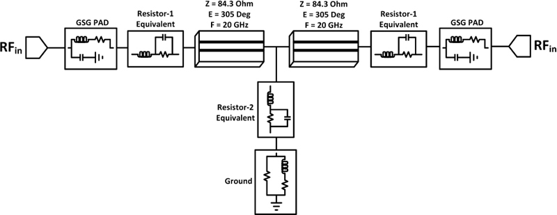
Figure 5: Schematic of 3 dB attenuator circuit model.
C. 2 dB, 4 dB, and 6 dB attenuator designs
The 2 dB, 4 dB, and 6 dB attenuators use the same distributed topology as shown in Fig. 6. All the designs have a flat response from DC to 40 GHz with less than 10 variation. The circuit is well-matched with a return loss value of better than 17 dB.
The circuit is designed as a fully symmetrical distributed Tee-type architecture. The resistor values are calculated according to equations (1) and (2) as seen in Fig. 1. The 2 dB attenuator has the series resistor R1T of 5.7 and the shunt resistor R2T of 215.2 . The 4 dB attenuator has the series, R1T of 11.3 , and the shunt resistor, R2T of 104.8 . The 6 dB attenuator has the series resistor, R1T, of 16.6 , and the shunt resistor, R2T, of 66.9 where the series resistors correspond to 0.66 squares, and the shunt resistors correspond to 1.34 squares of TFR resistors. The 2 dB attenuator layout is seen in Fig. 10 (b). The 4 dB attenuator layout is seen in Fig. 10 (d), and the 6 dB attenuator layout is seen in Fig. 10 (e).
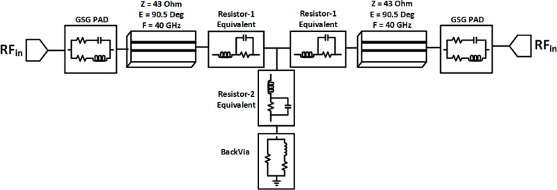
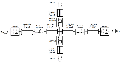
Figure 6: Schematic of 6 dB attenuator circuit model.
D. 10 dB and 12 dB attenuator designs
The 10 dB and 12 dB attenuators were designed with a tight variation of ±0.7 dB across the entire 40 GHz bandwidth using the same distributed topology. The flat insertion loss and good broadband matching performance are achieved by placing the resistors adjacent to each other and using low-impedance transmission lines for pad connections. The equivalent schematic is shown in Fig. 7. The shunt resistor splints into two parallel ones to achieve a broader response.
The resistor values are calculated as R1t26.0 and R2t35.1 for the 10 dB attenuator and R1t29.9 and R2t26.8 for the 12 dB attenuator according to equations (1) and (2). The series resistors correspond to 0.52 square, and the shunt resistors correspond to 0.7 square TFR resistors for the 10 dB attenuator. The 10 dB and 12 dB attenuator layouts are seen in Fig. 10 (f) and Fig. 10 (g), respectively.
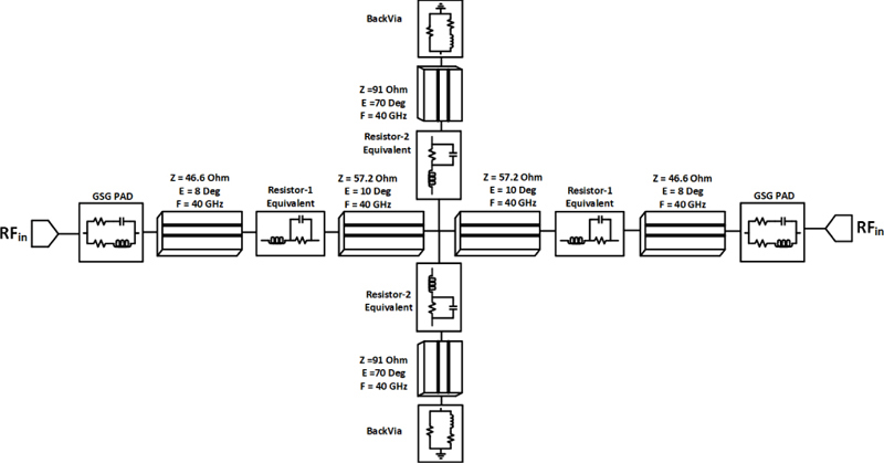
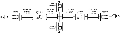
Figure 7: Schematic of 10 dB attenuator circuit model.
E. 20 dB and 30 dB attenuator designs
Both 20 dB and 30 dB attenuators were designed with a flatness target of ±1.6 dB throughout the frequency range. These designs are slightly larger than previous ones. The return losses are better than 20 dB. The shunt resistor in Tee-topology is distributed as two parallel resistors making it a cross-topology. The equivalent schematic for the 20 dB attenuator is shown in Fig. 9. The series and shunt resistors are 40.9 and 10 for the 20 dB attenuator. The EM simulation view of the 20 dB attenuator is given in Fig. 8. The 30 dB attenuator is realized as a cascade of two identical distributed cross topologies similar to the 20 dB one, where each one has 15 dB attenuation. The series resistors are 34.9 , and each parallel shunt resistor is 36.8 for the 15 dB attenuator. The 30 dB attenuator has four series and four shunt resistors. The 20 dB and 30 dB attenuator layouts are seen in Fig. 10 (h) and Fig. 10 (i), respectively.
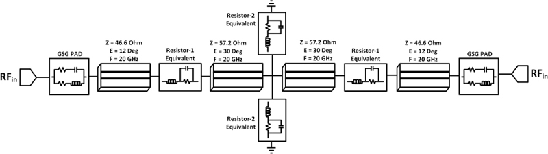
Figure 8: Schematic of 20 dB attenuator circuit model.
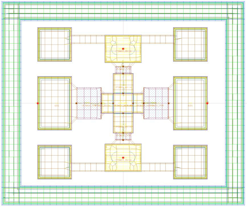
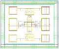
Figure 9: MoM-based EM view of 20 dB attenuator with meshes.
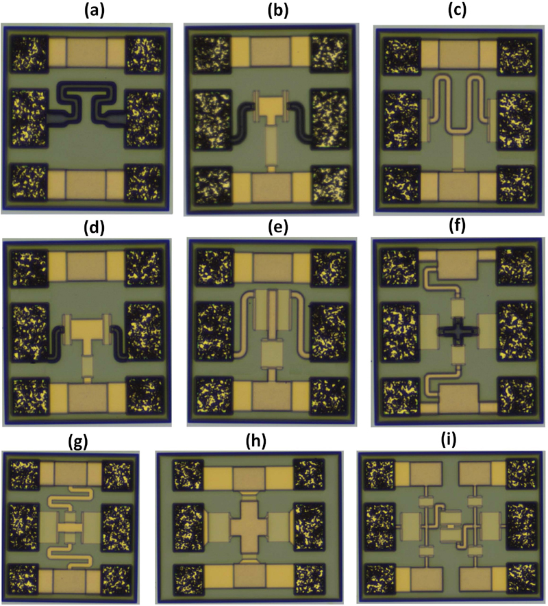
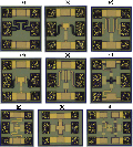
Figure 10: Die micrographs of (a) 0 dB, (b) 2 dB, (c) 3 dB, (d) 4 dB, (e) 6 dB, (f) 10 dB, (g) 12 dB, (h) 20 dB, and (i) 30 dB attenuators.
F. Die micrographs
The designed circuits were manufactured on a 6-inch 28V GaAs IPD process. The wafer has 112 reticles sized 10 mm 10 mm, including the process control monitors on the corners. The floor planning of the reticle is arranged to avoid sub-cuts and to yield the maximum number of dies. The photos of the selected circuits are shown in Fig. 10. The wafer is diced and placed on an expanded grip ring where the singulated dies remain in their original locations on the wafer. This allows a location-conscious measurement for determining the process spread across the wafer.
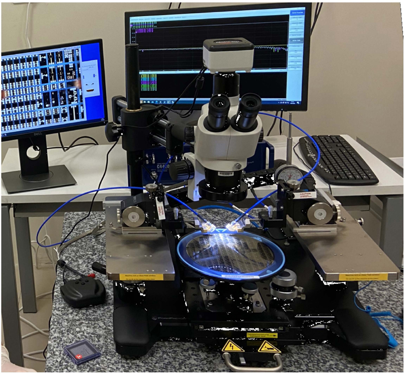
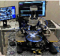
Figure 11: Probe station for die level measurement.
In Fig. 11, the FormFactor MPS150 probe station is used for measuring the singulated dies on various locations of the wafer. The pad metallization in the GaAs process is Au, which requires softer probe tips to avoid scratching and ensure better electrical contact. For this particular measurement, a pair of 150 m pitched Ground-Signal-Ground RF probes (Model 40A-GSG-150-P) with beryllium-copper tips are used. The measurements are taken using the Rohde & Schwarz ZVA67 Vector Network Analyzer, calibrated at the probe tips using the ISS 101-190 calibration substrate between DC and 40 GHz. The small signal measurements reported here are taken at room temperature, 25C.
G. 0 dB attenuator (THRU) results
Figure 12 has simulation and measurement results for the 0 dB attenuator, namely the THRU circuit. The measurement agrees with the simulation well for both insertion and return loss performance.
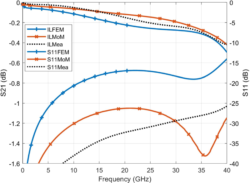
Figure 12: Sim vs Mea for 0 dB attenuator: (left) s21 in dB and (right) s11 in dB.
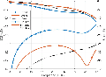
H. 3 dB attenuator result
Figure 13 shows the simulated and measured insertion loss and input reflection coefficient of the 3 dB attenuator. It is seen from the insertion loss plot that a 0.4 dB maximum variation is present. The measurement results were in good agreement with the full-chip electromagnetic simulations. The FEM simulations and the measurement results of the input reflection coefficient in dB for all designs are better than 22 dB.
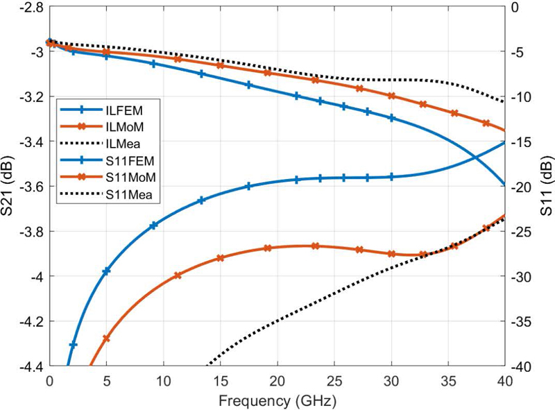
Figure 13: Sim vs Mea for 3 dB attenuator: (left) s21 in dB and (right) s11 in dB.
I. 4 dB and 6 dB attenuator results
Figure 14 has simulation and measurement results for the 4 dB attenuator. The 6 dB attenuator results are shown in Fig. 15. The simulated and measured insertion loss shows only a 0.6 dB variation across the frequency range.
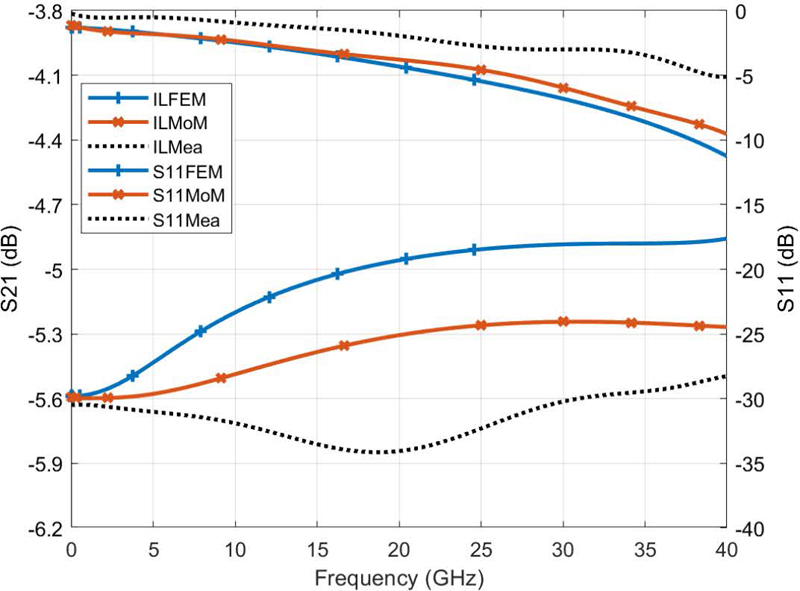
Figure 14: Sim vs Mea for 4 dB attenuator: (left) s21 in dB and (right) s11 in dB
The FEM simulations and the measurement results of the input reflection coefficient for all designs are better than 20 dB. The design’s distributed nature helped achieve such a wider frequency response.
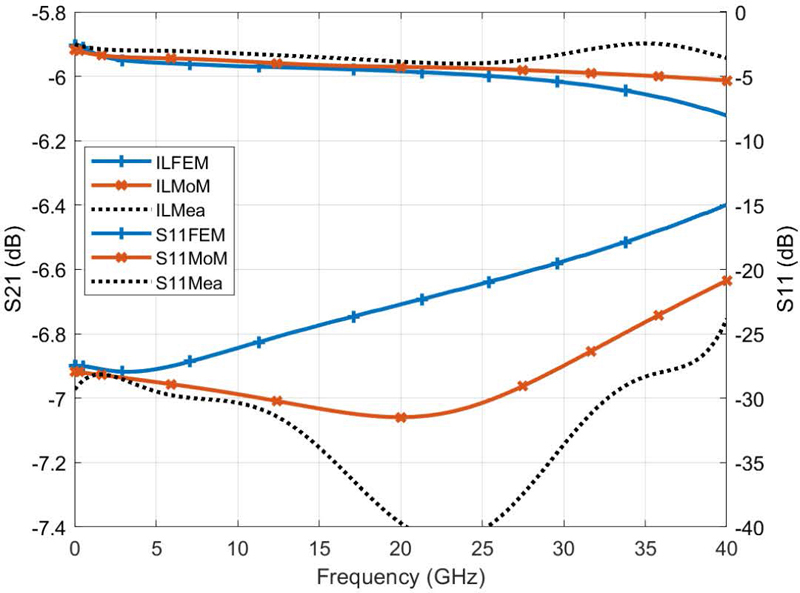
Figure 15: Sim vs Mea for 6 dB attenuator: (left) s21 in dB and (right) s11 in dB.
J. 10 dB and 12 dB attenuator results
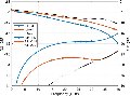
The simulated and measured performance plot of the 10 dB attenuator is shown in Fig. 16. The circuit has an ultra-flat broadband response with less than 0.25 dB variation from DC to 40 GHz, owning to its distributed design. The reflection coefficient is better than 22 dB. Insertion loss and return losses exceed the design targets and agree with the simulated performance.
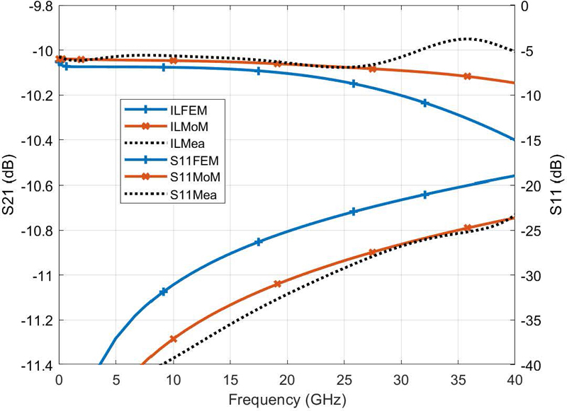
Figure 16: Sim vs Mea for 10 dB attenuator: (left) s21 in dB and (right) s11 in dB
Figure 17 has simulation and measurement results for the 12 dB attenuator.
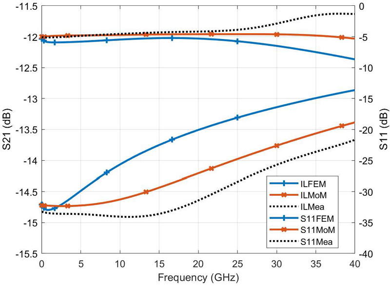
Figure 17: Sim vs Mea for 12 dB attenuator: (left) s21 in dB and (right) s11 in dB
K. 20 dB and 30 dB attenuator results
Figure 18 shows the simulated and measured results of the 20 dB attenuator with only a 0.48 dB variation across the band. The reflection coefficient is better than 23 dB for both measurement and FEM simulation. Figure 19 has simulation and measurement results for the 30 dB attenuator. Both designs have an ultra-flat response and highly matched behavior across the band.
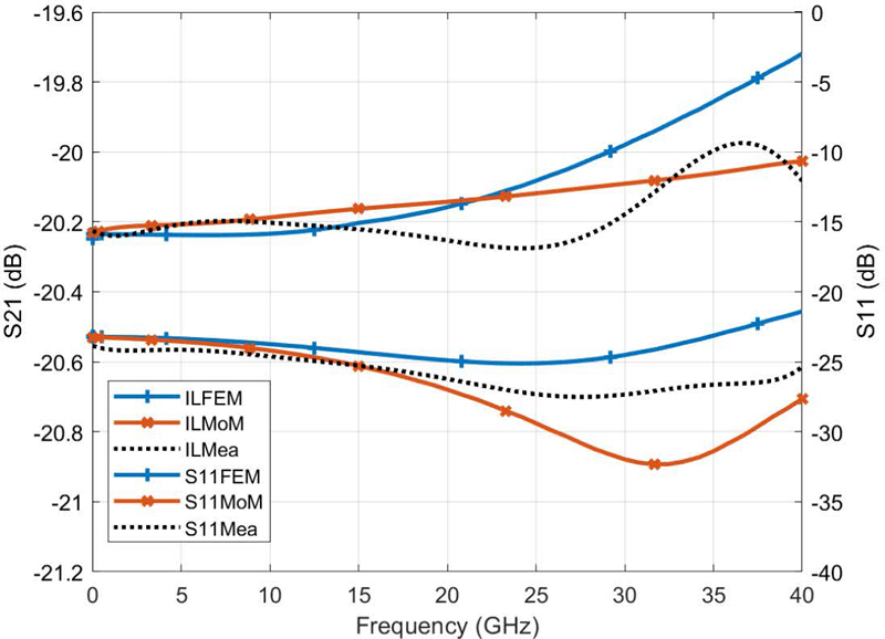
Figure 18: Sim vs Mea for 20 dB attenuator: (left) s21 in dB and (right) s11 in dB
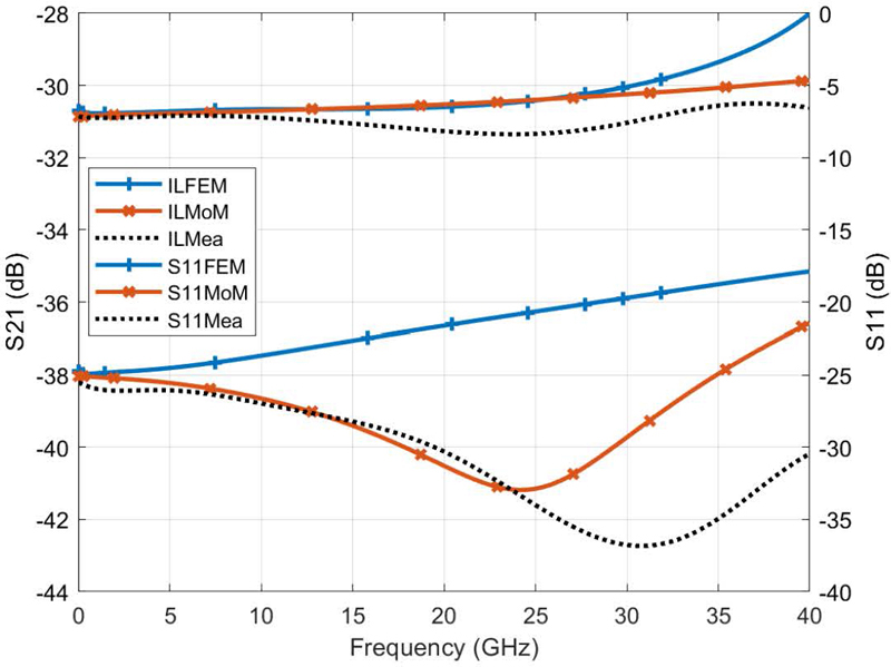
Figure 19: Sim vs Mea for 30 dB attenuator: (left) s21 in dB and (right) s11 in dB.
A comparison of this study and other published ones is demonstrated in Table 1. This study produced the most compact fixed attenuators to the best of the authors’ knowledge.
Table 1: Comparison of published fixed attenuators
| Ref | Atten | Freq | RL | Area | Process |
| (dB) | (GHz) | (dB) | (mm) | ||
| [29] | 3 /6 | DC-40 | 23 | 1 | GaAs |
| [29] | 20 | DC-40 | 24 | 2 | GaAs |
| [30] | 5 | DC-50 | 16 | 0.49 | Si |
| [31] | 20 | DC-20 | 27 | 0.45 | Si |
| [32] | 3 /6 | DC-18 | 18 | 4 | ThnFlm |
| [11] | 3 /6 | 5-40 | 15 | 0.35 | Graphn |
| Ours | 0 - 12 | DC-40 | 19 | 0.2 | GaAs |
| Ours | 20 / 30 | DC-40 | 24 | 0.27 | GaAs |
III. CONCLUSION
A family of Ka-band MMIC attenuator dies with different attenuation levels has been designed in GaAs-based IPD process using numerical analyses such as finite element method and Method of Moments. A classical attenuator topology is modified as a highly distributed network to fit in an ultra-compact area and to achieve the desired performance from DC to 40 GHz with the aid of a commercially available electromagnetic solver. The wafer-level s-parameter measurements are done at the probe station. The comparison of the different numerical solutions with the measurement data is also reported in the paper. The differences between the two solutions are due to the EM setup. The Method of Moments solution uses a finer mesh size and takes the edge and via effects into consideration; however, the finite element method is set up for faster simulation by trading the solution accuracy. The measurement results show a good agreement with the simulations and prove the viability of the design methodology.
ACKNOWLEDGMENT
The authors thank ASELSAN for the support and thank İbrahim Taha Gökçe for helping with the measurements.
REFERENCES
[1] J.-W. Jung, K.-K. Nae, J.-H. Bae, E.-J. Lee, H.-R. Oh, Y.-R. Seong, and J. Park, “Compact size directional coupler for mobile RFID reader,” in 2007 IEEE/MTT-S International Microwave Symposium, Honolulu, HI, pp. 987-989, 2007.
[2] S. Li, L. Ma, L. Wang, B. Wu, Y. Cheng, X. Lei, F. Liu, and G. J. Cheng, “An ultrawideband GaAs MMIC microstrip directional coupler with high directivity and very flat coupling,” IEEE Transactions on Microwave Theory and Techniques, vol. 70, no. 4, pp. 2271-2279, Apr. 2022.
[3] S. Hu and G. Qian, “Design of a miniature X-band broadband unequal power divider MMIC using bridged-T coils,” in 2021 International Applied Computational Electromagnetics Society (ACES-China) Symposium, Chengdu, China, pp. 1-2, 2021.
[4] Y. Chen, X. Yan, H. Wu, and L. Sun, “The design and miniaturization of 6-15 GHz lumped-element Wilkinson power divider based on GaAs IPD technology,” in 2018 IEEE Asia Pacific Conference on Circuits and Systems (APCCAS), Chengdu, China, pp. 207-210, 2018.
[5] K.-Y. Chen, B.-X. Fang, and H.-H. Yeh, “IPD broadband balun design for GSM applications,” in 2010 IEEE Electrical Design of Advanced Package & Systems Symposium, Singapore, pp. 1-4, 2010.
[6] Y. Lu, L. Shen, J. Wang, and Y. Shen, “The design of miniaturized broadband power divider utilizing GaAs-based IPD process and equivalent circuit model,” Chinese Institute of Electronics Journal of Semiconductors, vol. 38, no. 8, Aug. 2017.
[7] E. S. Kim, Y. Li, Z. Yao, and N. Y. Kim, “A compact Wilkinson power divider with high performance by GaAs-based optimized IPD process,” International Journal of Engineering and Technical Research, vol. 2, no. 10, Oct. 2014.
[8] X. Mi, T. Takahashi, and S. Ueda, “Integrated passives on LTCC for achieving chip-sized-modules,” in 2008 38th European Microwave Conference, Amsterdam, Netherlands, pp. 607-610, 2008.
[9] Y. Y. Zhu, Y.-J. Yang, and J.-X. Chen, “High performance bandpass filter using HTCC stepped-impedance resonators,” IET Microwaves, Antennas & Propagation, vol. 12, no. 1, pp. 56-62, Jan. 2018.
[10] P. Kuzhir, A. Paddubskaya, N. Valynets, K. Batrakov, T. Kaplas, P. Lamberti, R. Kotilkova, and P. Lambin, “Main principles of passive devices based on graphene and carbon films in microwave—THz frequency range,” Journal of Nanophotonics, vol. 11, no. 3, p. 032504, July 2017.
[11] K. Byun, Y. Ju Park, J.-H. Ahn, and B.-W. Min, “Flexible graphene-based microwave attenuators,” Nanotechnology, vol. 26 no. 5, p. 055201, Feb. 2015.
[12] K.-H. Lee, E.-S. Kim, J.-G. Liang, and N.-Y. Kim, “Design and realization of a compact high-frequency band-pass filter with low insertion loss based on a combination of a circular-shaped spiral inductor, spiral capacitor and interdigital capacitor,” Electronics, vol. 7, no. 9, p. 195, Sep. 2018.
[13] G. Shen, W. Che, W. Feng, Y. Shi, and Y. Shen, “Low insertion-loss MMIC bandpass filter using lumped-distributed parameters for 5G millimeter-wave application,” IEEE Transactions on Components, Packaging and Manufacturing Technology, vol. 11, no. 1, pp. 98-108, Jan. 2021.
[14] C.-Y. Hsiao, Y.-C. Huang, and T.-L. Wu, “An ultra-compact common-mode bandstop filter with modified-T circuits in Integrated Passive Device (IPD) process,” IEEE Transactions on Microwave Theory and Techniques, vol. 63, no. 11, pp. 3624-3631, Nov. 2015.
[15] K. W. Wong, R. R. Mansour, and G. Weale, “Reconfigurable bandstop and bandpass filters with wideband balun using IPD Technology for frequency agile applications,” IEEE Transactions on Components, Packaging and Manufacturing Technology, vol. 7, no. 4, pp. 610-620, Apr.2017.
[16] B. Lefebvre, A. Bessemoulin, H. Amara, R. Sevin, and P. Quentin, “High dynamic range, triple gate-based compact DC-40 GHz variable attenuator MMIC for Ka-band variable gain amplifier ICs,” in 25th Annual Technical Digest 2003. IEEE Gallium Arsenide Integrated Circuit (GaAs IC) Symposium, San Diego, CA, pp. 135-138, 2003.
[17] B. Khabbaz, A. Pospishil, E. R. Schineller, H. P. Singh, and J. Jorgenson, “DC-20 GHz MMIC multi-bit digital attenuators with on-chip TTL control,” in GaAs IC Symposium Technical Digest, Monterey, CA, pp. 239-242, 1991.
[18] R. Teja N. P. Verma, A. Kumar, and A. N. Bhattacharya, “A broadband high linearity voltage variable attenuator MMIC,” in 2015 6th International Conference on Computers and Devices for Communication (CODEC), Kolkata, India, pp. 1-4,2015.
[19] D. Hao, W. Zhang, X. Liu, and Y. Liu, “A wideband 6-bit digital attenuator in a GaAs pHEMT MMIC,” Electronics, vol. 11, no. 14, p. 2166, July 2022.
[20] R. Gupta, L. Holdeman, H. Carlson, J. Potukuchi, K. Hogan, and K. Pande, “Manufacturing technology and yield studies for MMIC 5-bit digital attenuators and phase-shifters,” in 12th Annual Symposium on Gallium Arsenide Integrated Circuit (GaAs IC), New Orleans, LA, pp. 305-308, 1990.
[21] G. Lizama, T. Andrade, and R. Benton, “1-6 GHz GaAs MMIC linear attenuator with integral drivers,” in Microwave and Millimeter-Wave Monolithic Circuits, Dallas, TX, pp. 105-107, 1987.
[22] H. Kondoh, “DC-50 GHz MMIC variable attenuator with a 30 dB dynamic range,” in IEEE MTT-S International Microwave Symposium Digest, New York, NY, pp. 499-502, 1988.
[23] Y. Tajima, T. Tsukii, R. Mozzi, E. Tong, L. Hanes, and B. Wrona, “GaAs monolithic wideband (2-18 GHz) variable attenuators,” in MTT-S International Microwave Symposium Digest, Dallas, TX, pp. 479-481, 1982.
[24] B. Maoz, “A novel, linear voltage variable MMIC attenuator,” IEEE Transactions on Microwave Theory and Techniques, vol. 38, no. 11, pp. 1675–1683, Nov. 1990.
[25] A. Aksen, E. G. Çimen, and B. S. Yarman, “A numerical real frequency broadband matching technique based on parametric representation of scattering parameters,” in IEEE APCCAS’98, Asia Pacific Conference on Circuits and Systems, Chiangmai, Thailand, pp. 351-354, 1998.
[26] B. S. Yarman and A. Fettweis, “Computer-aided double matching via parametric representation of Brune functions,” IEEE Transactions on Circuits and Systems, vol. 37, no. 2, pp. 212-222, Feb.1990.
[27] J. Lim, D. Kwon, J.-S. Rieh, S.-W. Kim, and S. W. Hwang, “RF characterization and modeling of various wire bond transitions,” IEEE Transactions on Advanced Packaging, vol. 28, no. 4, pp. 772-778, Nov. 2005.
[28] A. Sadigh, K. Kottapalli, and P. Petre, “EM simulation of packaged MMIC and microstrip antennas using ‘Microwave Explorer’,” ACES Journal, vol. 10, no. 3, pp. 146–152, Mar. 1995.
[29] A. S. Zagorodny, N. N. Voronin, I. V. Yunusov, G. G. Goshin, A. V. Fateev, and A. Y. Popkov, “Microwave microstrip attenuators for GaAs monolithic integrated circuits,” in International Conference and Seminar of Young Specialists on Micro/ Nanotechnologies and Electron Devices, Altai, Russia, pp. 67-71, 2012.
[30] L. Dong, Y. Huang and X. Chen, “Novel silicon-based attenuator chip,” in IEEE 4th International Conference on Electronics and Communication Engineering (ICECE), Xi’an, China, pp. 324-329, 2021.
[31] Q. Zhong, X. Liang, and Z. Liu, “Design of single thin film resistor network as 20dB attenuator for DC-20GHz application,” in 16th International Conference on Electronic Packaging Technology (ICEPT), Changsha, China, pp. 297-300, 2015.
[32] H. J. Finlay, L. G. T. Hopkins, and J. M. Ozamiz, “Design and applications of precision microstrip multioctave attenuators and loads,” in 6th European Microwave Conference, Rome, Italy, pp. 692-696, 1976.
BIOGRAPHIES

Mehmet Emin Bayrak received his B.S. degrees in both Biomedical Engineering and Electrical & Electronics Engineering as double major in 2019 and 2020, respectively. He graduated with M.S. degree from Electrical Electronics Engineering and Cyber Systems program at Istanbul Medipol University in 2022. His master’s thesis was on passive MMIC devices. Since 2021, he has been working at TUBITAK, BILGEM as a Researcher. His research interests are III-V-based active and passive MMIC design.

Harun Tekin was born in Istanbul, Turkey, in 1997. He received his B.S. in Electrical & Electronics Engineering from Istanbul Medipol University, Istanbul, Turkey, in 2020. He is currently pursuing an M.S. student in the Electrical Electronics Engineering and Cyber Systems program at Istanbul Medipol University. Since 2022, he has been working as an RF Hardware Design Engineer at NETA Communications. His research topics are the design of passive MMIC, antennas, receiver, and transmitter systems.

Huseyin Serif Savci received the B.S. in Electronics & Communication Engineering from Yildiz Technical University, Istanbul, Turkey in 2001 and the M.S. and Ph.D. degrees in Electrical Engineering from Syracuse University, Syracuse, NY, USA, in 2005 and 2008, respectively. From 2008 to 2013, he was with Skyworks Solutions Inc., Cedar Rapids, IA, USA, as a Senior RFIC Design Engineer. Between 2013 and 2020, he worked as a Principal Design Engineer for Hittite Microwave Corporation, Chelmsford, Massachusetts, and Analog Devices Inc., Istanbul, Turkey. Over the years, he designed and released many RFIC and MMIC products on CMOS, SiGe, SOI, GaN, and GaAs technologies. He is currently an Associate Professor in the Department of Electrical and Electronics Engineering at Istanbul Medipol University, Istanbul, Turkey. He leads the RFMicroSense Research Group, which focuses on the design and modeling of RF and Microwave Integrated Circuits, devices, systems, and antennas. He is also an Associate Editor for the Applied Computational Electromagnetics Society.
ACES JOURNAL, Vol. 39, No. 7, 658–667
doi: 10.13052/2024.ACES.J.390710
© 2024 River Publishers