Compact-size Lightweight Beam-reconfigurable ESPAR Antenna with Parasitic Elements for UAV Applications
Min-Jae Kang, Yu-Seong Choi, and Wang-Sang Lee
1Department of Electrical Engineering
Gyeongsang National University (GNU), B405-401, 501, Jinju-daero, Jinju-si, Gyeongnam,
52828, Republic of Korea
hunt0919@gnu.ac.kr, wsang@gnu.ac.kr
*Corresponding author
2Korea Aerospace Industries (KAI), Ltd
78, Gongdan 1-ro, Sanam-myeon, Sacheon-si, Gyeongnam, 52529, Republic of Korea
cys4140@gnu.ac.kr
Submitted On: May 17, 2024; Accepted On: July 5, 2024
ABSTRACT
This paper presents a compact lightweight beam-reconfigurable antenna system for unmanned aerial vehicles (UAVs). The antenna system consists of a central active monopole element surrounded by eight parasitic elements, which can be controlled using PIN diodes to switch the beam across four elevation angles and eight azimuth beams. This beam-reconfigurable antenna system has several advantages over traditional UAV antennas, including light weight, efficiency, and compactness. The antenna system operates at 5.09 GHz and achieves a measured peak gain of 4.55 dBi, with a remarkably low weight of 9 g and a size of 1.001.000.22.
Index Terms: Beam-reconfigurable, compact, electronically steerable parasitic array radiator (ESPAR) antenna, PIN didoes, UAV applications.
I. INTRODUCTION
Unmanned aerial vehicles (UAVs) are increasingly being used in various military applications and mission scenarios, as they offer several advantages over traditional aircraft, including flexibility, maneuverability, and cost-effectiveness. In the context of the Fourth Industrial Revolution, UAVs are expected to play an even more critical role in diverse fields such as logistics, disaster relief, and environmental monitoring. One of the key challenges in designing UAVs is developing efficient and compact communication systems. Reconfigurable antennas offer a promising solution to this challenge, as they can dynamically adjust their radiation patterns to adapt to changing environmental conditions and communication requirements [1–8].
Electronically Steerable Parasitic Array Radiator (ESPAR) is a well-known type of reconfigurable antenna that has been widely studied for UAV applications. ESPAR antennas consist of a central active radiating element surrounded by passive radiating elements. The passive elements play a crucial role in reflecting or re-radiating the waves emitted by the central active element. The re-radiation process is controlled by variable loads or switches that are connected to each passive element. By adjusting the loads applied to the passive elements, it is possible to alter the phase of the re-radiated waves. This allows for precise control over the radiation pattern and direction of the entire antenna array [9–19].
In this paper, we propose a modified ESPAR antenna design for UAV applications. The modified design enables precise control over both azimuth and elevation angles, facilitating enhanced beam steering capabilities at a center frequency of 5.09 GHz.
II. BACKGROUND THEORY
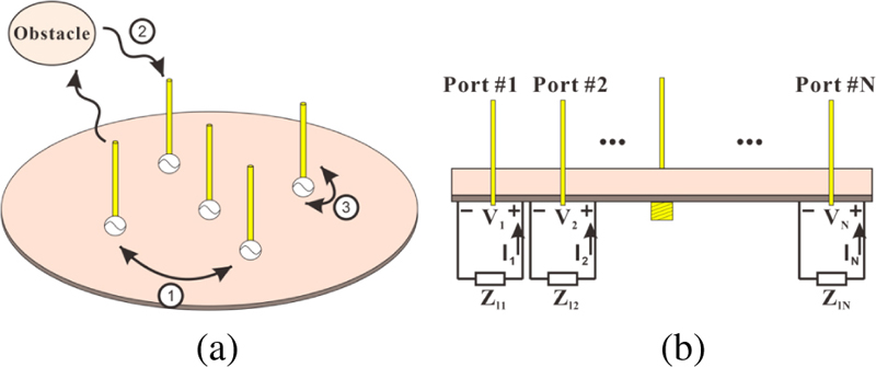
This section provides the theoretical foundation to comprehend the fundamental principles behind the functioning of the proposed antenna. To begin with, there are three mechanisms responsible for the mutual coupling in a multi-element ESPAR antenna, as depicted in Fig. 1 (a) [20]. These mechanisms include (1) direct spatial coupling between elements, (2) indirect coupling that can occur through scattering from nearby objects, such as support towers, and (3) a feed network that provides a pathway for coupling. Furthermore, there are elements in the multi-element antenna that do not generate their own current. Instead, they have significant currents induced by radiation from neighboring elements. These elements are referred to as parasitic elements, which have a significant impact on the performance of an antenna system that includes them. Let’s consider ESPAR antenna consisting of one active element and (N-1) passive elements (a total of N elements). This ESPAR antenna can be represented as an N-port network, as shown in Fig. 1 (b). The voltages and currents at the feeding point of each element can be defined using the following equation:
| (1) |
where ,, and represent the voltage, current, and self-impedance of the kth element, and represents the mutual impedance between the kth and ith elements. The variables k and i 1, 2, …N. In ESPAR antenna, the parasitic elements are typically terminated with reactive loads, short circuits (SC), or open circuits (OC). Therefore, in a general form, we can consider them loaded with complex impedances denoted as . Thus, the voltage of parasitic ports is expressed as:
| (2) |
where represents the impedance load of the kth element. By substituting (2) into (1), the matrix form can be obtained as in (3):
| (3) |
Figure 1: (a) Mechanisms for coupling between elements of a multi-element antenna and (b) a side view of the multi-port network representing the mutual coupling between active and parasitic elements.
The Method of Moments (MoM) and the Finite Element Method (FEM) are the most commonly used numerical methods for computing the mutual impedance matrix in (3) then the elements’ currents can be determined as given in (4):
| (4) |
The mutual impedance matrix governs the magnitude, phase, and distribution of the elements’ currents for the ESPAR antenna. The total field pattern of an N-element ESPAR antenna is the superposition of all elements’ radiation patterns and can be obtained by (5). In this ESPAR antenna, the parasitic elements are arranged in a circular pattern around the active element [21]:
| (5) |
where the angular position of the kth element is denoted by represents the position vector of the kth element is the unit vector toward the observation point. is the radiation patteren of the active element is the field pattern of the single kth element. is the phase constant. d is the distance between the active element and each passive element. is the complex current excitation coefficient of the kth element. This current coefficient includes both magnitude and phase information, enabling precise control of the antenna’s radiation pattern. The phase of these current coefficients determines the direction of maximum power radiation, while the magnitude influences the directivity, gain, and coverage characteristics of the antenna. In this paper, four different modes (Mode A, Mode B, Mode C, and Mode D) have been developed to generate multiple beams in the azimuth and elevation directions. Each mode can be constructed by activating one or more of the PIN diodes connected to the passive elements. The activation of the PIN diode connected to the kth passive element impacts its complex load impedance. Therefore, its complex current excitation coefficient varies, resulting in different beam directions as described in (5).
III. ANTENNA CONFIGURATION
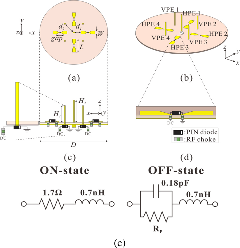
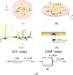
The proposed antenna consists of a central active element, which is a monopole, surrounded by passive elements, as illustrated in Figs. 2 (a-c). The active element at the center is fed by an RF signal, while the neighboring passive elements can either be connected or disconnected to the ground using the PIN diodes. The PIN diodes (SMP1331-079LF), which have a forward bias voltage of 0.8 V and reverse current of 10 A have been selected for implementation with the passive elements due to their high-power handling, switching, and low insertion loss characteristics [22, 23]. Figure 2 (e) shows the equivalent circuit of the PIN diode. The resistance in the ON state (1.7 ) can cause RF losses. In ESPAR antennas, beam steering can be achieved by configuring the passive elements using the PIN diodes. The passive elements consist of bow-tie-shaped HPEs and monopole-shaped VPEs forming an antenna structure. Each of these elements is controlled by PIN diodes. Crucial parameters for impedance matching include the distance between the active element and VPEs, as well as the height of the VPEs. Increasing the distance improves the reflection coefficient, while increasing the height raises the operational frequency and narrows the bandwidth. When the PIN diodes are activated, the HPEs’ arms connect, resulting in resonance at 5.09 GHz. These effectively act as reflectors. Similarly, when the PIN diodes of the VPEs are activated, they act as directors.
Figure 2: Proposed antenna configuration: (a) a top view, (b) a perspective view, (c) a side view, (d) a HPE cutting plane view with a diode junction diagram, and (e) on/off equivalent model of the PIN diode.
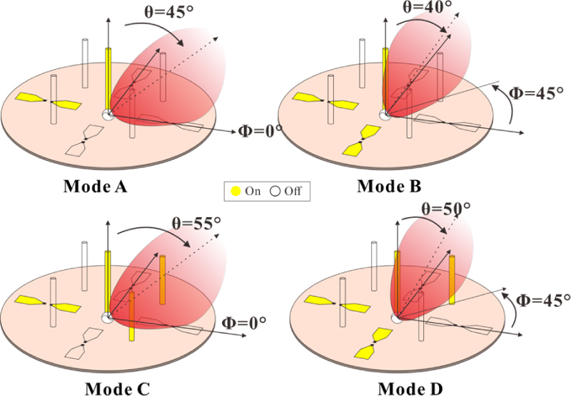
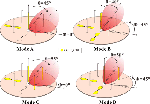
Figures 3 and 4 show that the number of activated passive elements controlled by PIN diodes determines the mode, and the simulated 3D gain patterns for Modes A, B, C, and D.
Figure 3: Schematic diagram according to the operation of parasitic elements.
Figure 4: Simulated 3-D realized gain patterns of different modes: (a) Mode A, (b) Mode B, (c) Mode C, and (d) Mode D.
The primary difference among modes lies in the elevation angle. In Mode A, the antenna uses a single HPE for beam steering and achieves azimuth angles of , , , and . The key feature of Mode A is that HPEs act as reflectors. In this mode, the antenna steers the beam in four different azimuth directions while maintaining an elevation angle of . This means that the antenna’s beam is tilted upward from the horizontal plane. Mode B offers specific beam steering capabilities, using only two HPEs for achieving azimuth angles of ,, and . Similar to Mode A, Mode B maintains a consistent elevation. Mode C employs one HPE and two VPEs for beam steering, achieving azimuth angles of , , , and . The presence of two VPEs helps to provide more precise beam direction while maintaining a relatively higher elevation angle of Mode D, the final operating mode, uses two HPEs and one VPE for beam steering at azimuth angles of , , , and . Similar to Mode B, this mode allows for diagonal beam steering, providing directional flexibility. This is particularly valuable when the target or communication point is not aligned with the primary azimuth points. One of the challenges in antenna design, especially when incorporating active components like PIN diodes, is managing potential interference between DC and RF signals. Such interference can degrade antenna performance, resulting in inconsistent radiation patterns and reduced efficiency. Figure 2 (d) shows how to address this challenge by integrating a chip inductor into the antenna design. This inductor, known as an RF choke, is connected in parallel to the HPE arm. Its purpose is to facilitate the smooth flow of the DC signal required to control the PIN diode while isolating it from the RF signal. This separation ensures that the DC signal does not interfere with the RF signal, enabling consistent and optimal antenna performance. The antenna’s design philosophy prioritizes both performance and structural simplicity. A simple design expedites manufacturing, reduces potential points of failure, and often leads to cost savings. To align with this philosophy, the placement of the RF choke inductor has been carefully selected. Instead of introducing an external component or a complex network, the inductor was positioned directly on the substrate. This was achieved by drilling a via at the junction of the HPE arm and the PIN diode. This strategic placement minimizes the length of the signal path, thereby reducing signal losses and ensuring efficient operation. Additionally, this placement contributed to a compact design.
IV. RESULTS AND DISCUSSION
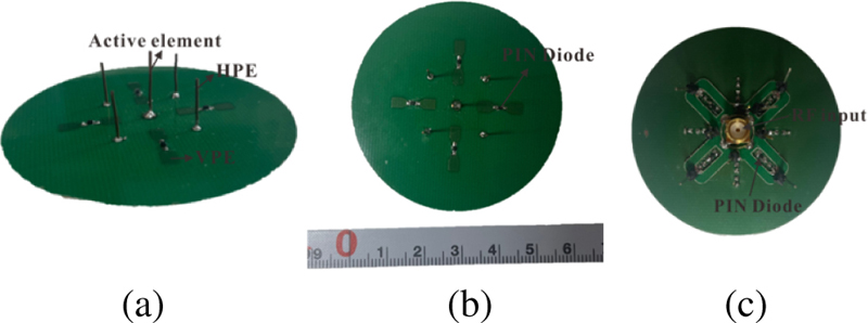
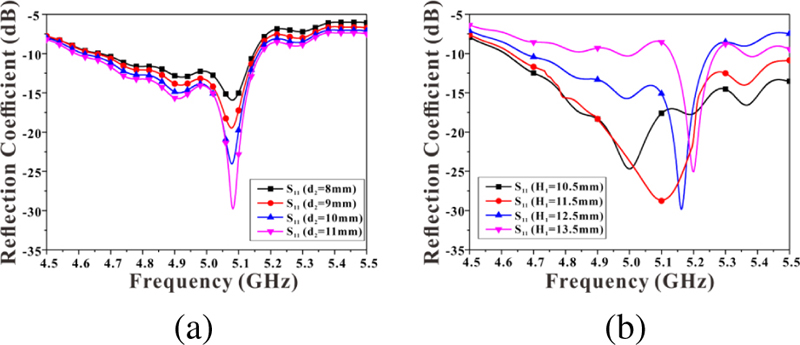
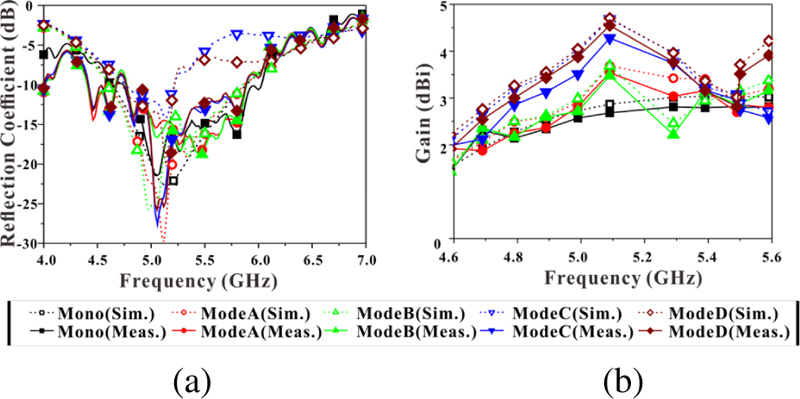
For the experimental verification, the substrate of the proposed antenna is used in the TACONIC RF-35 which has a dielectric constant () of 3.5, and loss tangent (tan ) of 0.0018. The substrate has a thickness of 0.76 mm, and the thickness of the copper layer is 0.018 mm. Figure 5 shows the fabricated proposed antenna. The optimal parameters of the proposed antenna are shown in Table 1. These design parameters define the structure of the proposed antenna, which has a significant impact on its radiation pattern and frequency response. For instance, and represent the distances between elements in the proposed antenna, while and denote the height of the elements. D, L, and W determine the size and shape of the antenna, and the selection of these parameters is crucial in achieving the desired antenna performance. In Figs. 6 (a-b), simulation results are presented based on design parameters related to the most critical aspect of the proposed antenna, namely VPE. As the distance () between the central active element and VPE increases, the reflection coefficient improves. Additionally, when the height of VPE () is increased, the operating frequency shifts to higher frequency bands, resulting in a narrower bandwidth. The comparison of simulated and measured results for various operating modes of the proposed antenna underscores its versatility and flexibility. Figure 7 (a) illustrates the measured 10-dB bandwidth of the proposed antenna, which spans from 4.61 GHz to 5.86 GHz. The operating frequency range of the proposed antenna makes it suitable for a wide range of applications. The measurements of the S-parameters were carried out using a vector network analyzer by Rohde & Schwarz (RS-ZND 40). The simulated and measured gains are shown in Fig. 7 (b), a peak gain of approximately 4.55 dBi can be obtained when Mode D is selected. The discrepancy between the simulated and measured results is attributed to the use of PIN diodes. PIN diodes exhibit non-ideal behavior in real-world applications, including parasitic inductance, resistance, and capacitance, which are often simplified or neglected in simulations. Consequently, PIN diodes can introduce additional impedance variations and losses that are difficult to accurately model in simulations. Modes C and D exhibit higher discrepancies between the simulated and measured results because they utilize more PIN diodes compared to the other proposed modes.
Figure 5: Fabricated proposed antenna: (a) a perspective view, (b) a top view, and (c) a bottom view.
Figure 6: Simulated impedance characteristics of the proposed antenna with regard to the design parameters: (a) impedance characteristics in regard to the distance () between active element and VPE and (b) impedance characteristics in regard to the height () of VPE.
Table 1: Geometric design parameters of the proposed antenna (unit mm)
| W | L | ||
|---|---|---|---|
| 6 | 13 | 2.8 | 12.28 |
| D | |||
| 6 | 10.5 | 13.3 | 58.93 |
Figure 7: The characteristics of the proposed antenna at operating mode.
Table 2: Comparison of the proposed antenna parameters with other antenna designs
| Antenna Parameters | [14] | [15] | [16] | [17] | [18] | Prop. | |
| 2.055 | 2.45 | 2.484 | 2.44 | 5.09 | 5.09 | ||
| BW (%) | 2.6 | 16 | N/A | N/A | 8.6 | 12.7 | |
| Peak gain (dBi) | 4.58 | N/A | 5.3 | 8.1 | 4.9 | 4.55 | |
| Num. of Az.Beams | 2 | 15 | 12 | 6 | 8 | 8 | |
| Num. of Ele.Beams | 2 | 3 | 1 | 3 | 1 | 4 | |
| Num. of Act.Elem. | 4 | 1 | 1 | 1 | 1 | 1 | |
| Num. of Para.Elem. | 4 | 8 | 12 | 12 | 8 | 8 | |
| Elect. Size () |
L () | 1.21 | 1.63 | 1.26 | 1.06 | 1.00 | 1.00 |
| W () | 1.17 | 1.63 | 1.26 | 1.06 | 1.00 | 1.00 | |
| H () | 0.05 | 0.26 | 0.25 | 0.36 | 0.25 | 0.22 | |
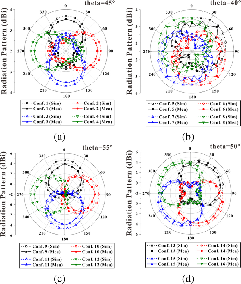
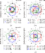
Figure 8: Radiation pattern with regard to the operating modes at 2D cutting plane: (a) Mode A at , (b) Mode B at , (c) Mode C at , and (d) Mode D at .
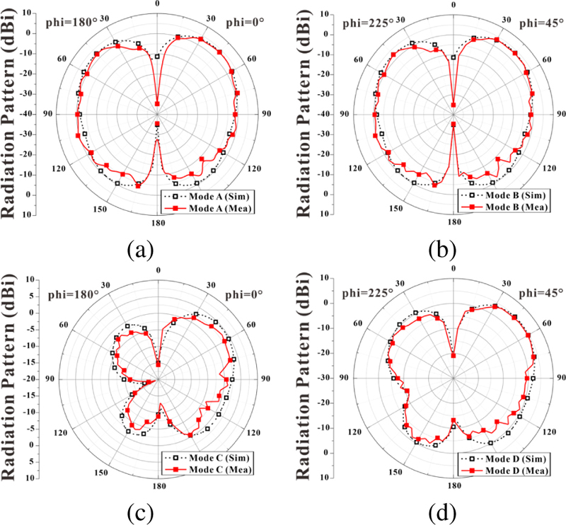
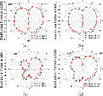
Figure 9: Radiation pattern by operating mode at 2D cutting plane: (a) Mode A, (b) Mode B, (c) Mode C, and (d) Mode D.
Figures 8 (a-d) illustrates the comparison between simulation and measurement values for the azimuth angles for each mode. In each operational mode, the configuration was systematically classified based on distinct azimuth angles. These radiation patterns in Modes A to D demonstrate the antenna’s ability to steer the beam in specific directions, offering precise directionality required in various application scenarios.
Modes A and C exhibit azimuth angles of , , , and , while Modes B and D show angles of , , , and . As previously mentioned, equivalent resistors in the PIN diodes cause RF losses. Since the proposed antenna utilizes up to three PIN diodes in a single mode, the actual measured gain of the antenna exhibits some discrepancies from the simulated gain. Figs. 9 (a-d) illustrate a comparison of elevation angles for all beam patterns from Mode A to Mode D. With a single reflector (HPE), Mode A has an elevation angle of . Mode C with added VPEs achieves a maximum elevation angle of . Mode B, with two reflectors, maintains a elevation angle, while Mode D, featuring an additional VPE, reaches an elevation angle of . The proposed antenna has the highest number of elevation-beams compared to the other antenna designs. Furthermore, the performance of the proposed antenna, in terms of compact size, wide bandwidth, high gain, simple structure, and a high number of azimuth-beams, is comparable to that of the previous antenna designs, as indicated in Table 2. Compared to the other antenna designs in Table 2, the proposed antenna has the smallest size. When compared to [17] and [18], which also utilize a single active element, the proposed antenna uses fewer parasitic elements while achieving control over two additional azimuth angles and one additional elevation angle compared to [17]. Despite having the same number of parasitic elements as [18], the proposed antenna can control four elevation angles, unlike [18], which cannot control elevation angles.
V. CONCLUSION
A 5.09 GHz beam-reconfigurable antenna for U2X communications is presented in this paper. The proposed antenna consists of VPEs and HPEs parasitic elements, each using PIN diodes, and it switches the beam direction to eight azimuth and four elevation angles. This indicates that fewer parasitic elements are used compared to the number of reconfigurable modes, while still using a small number of active elements. The RF choke of this antenna is inserted through via in the substrate, making it more compact and reducing signal loss, thus increasing efficiency. The antenna was fabricated and tested in an anechoic chamber, and the results show that the antenna achieves a peak gain of 4.55 dBi and a low weight of 9 g. The proposed antenna design has the potential to significantly improve the communication, radar, and search and rescue capabilities of UAVs. It is also lightweight and compact, making it ideal for UAV applications.
ACKNOWLEDGMENT
This work was supported in part by the Korean Government (MSIT) through the National Research Foundation of Korea, South Korea, under Grant RS-2024-00338277, in part by the Institute of Information & Communications Technology Planning & Evaluation (IITP) grant funded by the Korea government (MSIT), under Grant RS-2022-00156409 (ICT innovation human resources 4.0).
REFERENCES
[1] F. Grimaccia, F. Bonfante, M. Battipede, P. Maggiore, and E. Filippone, “Risk analysis of the future implementation of a safety management system for multiple RPAS based on first demonstration flights,” Electronics, vol. 6, no. 3, pp. 50, 2017.
[2] H. Baek and J. Lim, “Design of future UAV-relay tactical data link for reliable UAV control and situational awareness,” IEEE Communications Magazine, vol. 56, no. 10, pp. 140-150, 2018.
[3] H. Ullah, N. G. Nair, A. Moore, C. Nugent, P. Muschamp, and M. Cuevas, “5G communication: An overview of vehicle-to-everything, drones, and healthcare use-cases,” IEEE Access, vol. 7, pp. 37251-37268, 2019.
[4] R. Kovalchukov, D. Moltchanov, A. Samuylov, and A. Ometov, “Analyzing effects of directionality and random heights in drone-based mmwave communication,” IEEE Transactions on Vehicular Technology, vol. 67, no. 10, pp. 10064-10069, 2018.
[5] S. A. R. Naqvi, S. A. Hassan, H. Pervaiz, and Q. Ni, “Drone-aided communication as a key enabler for 5G and resilient public safety networks,” IEEE Communications Magazine, vol. 56, no. 1, pp. 36-42, 2018.
[6] M. S. Sharawi, O. A. Rawashdeh, and D. N. Aloi, “Performance of an embedded monopole antenna array in a UAV wing structure,” in Melecon 2010 - 2010 15th IEEE Mediterranean Electrotechnical Conference, Valletta, Malta, pp. 835-838, 2010.
[7] X. Miao, W. Wan, Z. Duan, and W. Geyi, “Design of dual-mode arc-shaped dipole arrays for indoor base-station applications,” IEEE Antennas and Wireless Propagation Letters, vol. 18, no. 4, pp. 752-756, 2019.
[8] C. U. Lee, G. Noh, B. Ahn, J.-W. Yu, and H. L. Lee, “Tilted-beam switched array antenna for UAV mounted radar applications with 360 coverage,” Electronics, vol. 8, no. 11, pp. 1240, 2019.
[9] M. Taromaru and T. Ohira, “Electronically steerable parasitic array radiator antenna: Principle control theory and its applications,” Proc. Int. Union of Radio Science General Assembly, 2005.
[10] R. Harrington, “Reactively controlled directive arrays,” IEEE Transactions on Antennas and Propagation, vol. 26, no. 3, pp. 390-395, 1978.
[11] T. Ohira and K. Iigusa, “Electronically steerable parasitic array radiator antenna,” Electronics and Communications in Japan (Part II: Electronics), vol. 87, no. 10, pp. 25-45, 2004.
[12] C. Sun, A. Hirata, T. Ohira, and N. C. Karmakar, “Fast beamforming of electronically steerable parasitic array radiator antennas: Theory and experiment,” IEEE Transactions on Antennas and Propagation, vol. 52, no. 7, pp. 1819-1832, 2004.
[13] J. Costantine, Y. Tawk, S. E. Barbin, and C. G. Christodoulou, “Reconfigurable antennas: Design and applications,” Proceedings of the IEEE, vol. 103, no. 3, pp. 424-437, 2015.
[14] S. V. S. Nair and M. J. Ammann, “Reconfigurable antenna with elevation and azimuth beam switching,” IEEE Antennas and Wireless Propagation Letters, vol. 9, pp. 367-370, 2010.
[15] Z. Shi, R. Zheng, J. Ding, and C. Guo, “A novel pattern-reconfigurable antenna using switched printed elements,” IEEE Antennas and Wireless Propagation Letters, vol. 11, pp. 1100-1103, 2012.
[16] M. Groth, M. Rzymowski, K. Nyka, and L. Kulas, “ESPAR antenna-based WSN node with DoA estimation capability,” IEEE Access, vol. 8, pp. 91435-91447, 2020.
[17] M. Rzymowski and L. Kulas, “Two-row ESPAR antenna with simple elevation and azimuth beam switching,” IEEE Antennas and Wireless Propagation Letters, vol. 20, no. 9, pp. 1745-1749, 2021.
[18] Y.-S. Choi and W.-S. Lee, “Reconfigurable beam switching antenna with horizontal parasitic element reflector (HPER) for UAV applications,” in 2020 IEEE International Symposium on Antennas and Propagation and North American Radio Science Meeting, Montreal, QC, Canada, pp. 433-434, 2020.
[19] H. Kawakami and T. Ohira, “Electrically steerable passive array radiator (ESPAR) antennas,” IEEE Antennas Propag. Mag., vol. 47, no. 2, pp. 43-50, Apr. 2005.
[20] R. Movahedinia, “Low-cost beam steerable antennas using parasitic elements,” Dissertation, Concordia University, 2018.
[21] C. A. Balanis, Antenna Theory: Analysis and Design. Hoboken, NJ: Wiley, 2016.
[22] C. G. Christodoulou, Y. Tawk, S. A. Lane, and S. R. Erwin, “Reconfigurable antennas for wireless and space applications,” Proceedings of the IEEE, vol. 100, no. 7, pp. 2250-2261, 2012.
[23] D. Piazza, P. Mookiah, M. D’Amico, and K. R. Dandekar, “Experimental analysis of pattern and polarization reconfigurable circular patch antennas for MIMO systems,” IEEE Transactions on Vehicular Technology, vol. 59, no. 5, pp. 2352-2362, 2010.
BIOGRAPHIES

Min-Jae Kang received the B.S. degrees in electronic engineering from Gyeongsang National University (GNU), Jinju, South Korea, in 2023. His research interests are reconfigurable antennas for unmanned aeronautics, wireless power transfer, high-power microwave systems, and communications systems, RFID/IoT sensors, and RF/microwave circuit and antenna designs.

Yu-Seong Choi received the B.S. and the M.S. degrees in electronic engineering from Gyeongsang National University (GNU), Jinju, South Korea, in 2019 and 2021, respectively. Since 2022, he is currently working in Korea Aerospace Industries.
His research interests include reconfigurable antenna design & analysis, RF/Microwave circuits and systems, and RFID/IoT sensors.

Wang-Sang Lee received the B.S. degree from Soongsil University, Seoul, South Korea, in 2004, and the M.S. and Ph.D. degrees in electrical engineering from the Korea Advanced Institute of Science and Technology (KAIST), Daejeon, South Korea, in 2006 and 2013, respectively.
From 2006 to 2010, he was with the Electromagnetic Compatibility Technology Center, Digital Industry Division, Korea Testing Laboratory (KTL), Ansan-si, South Korea, where he was involved in the international standardization for radio frequency identification (RFID) and photovoltaic systems as well as electromagnetic interference (EMI)/EMC analysis, modeling, and measurements for information technology devices. In 2013, he joined the Korea Railroad Research Institute (KRRI), Uiwang-si, South Korea, as a Senior Researcher, where he was involved in the position detection for high-speed railroad systems and microwave heating for low-vibration rapid tunnel excavation system. Since 2014, he has been an Associate Professor with the Department of Electronic Engineering, Gyeongsang Nat’l University (GNU), Jinju, South Korea. From 2018 to 2019, he was a Visiting Scholar with the ATHENA Group, Georgia Institute of Technology, Atlanta, GA, USA. His current research interests include near- and far-field wireless power and data communications systems, RF/microwave antenna, circuit, and system design, RFID/Internet of Things (IoT) sensors, and EMI/EMC.
Dr. Lee is a member of IEC/ISO JTC1/SC31, KIEES, IEIE, and KSR. He was a recipient of the Best Paper Award at IEEE RFID in 2013, the Kim Choong-Ki Award Electrical Engineering Top Research Achievement Award at the Department of Electrical Engineering, KAIST, in 2013, the Best Ph.D. Dissertation Award at the Department of Electrical Engineering, KAIST, in 2014, the Young Researcher Award at KIEES in 2017, and the Best Paper Awards at IEIE in 2018 and KICS in 2019.
ACES JOURNAL, Vol. 39, No. 5, 433–439
doi: 10.13052/2024.ACES.J.390507
© 2024 River Publishers
