Accelerated Extraction of Parasitic Capacitance in Metal Interconnects using Floating Random Walk Method
Dongyan Zhao, Yanning Chen, Fang Liu, Yang Zhao, Yali Shao, Dong Zhang, Yucheng Pan, and Xiangyu Meng
1State Grid Key Laboratory of Power Industrial Chip Reliability Technology
Beijing Smartchip Microelectronics Technology Co. Ltd., 100192, China
dongyan-zhao@sgchip.sgcc.com.cn, chenyanning@sgchip.sgcc.com.cn, liufang@sgchip.sgcc.com.cn, zhaoyang@sgchip.sgcc.com.cn, shaoyali@sgchip.sgcc.com.cn, zhangdong@sgchip.sgcc.com.cn
2School of Electronics and Information Technology
Sun Yat-sen University, 510006, China
panych7@mail2.sysu.edu.cn, mengxy26@mail.sysu.edu.cn
Submitted On: May 8, 2024; Accepted On: December 3, 2024
ABSTRACT
This paper presents a novel and efficient approach for the rapid extraction of parasitic capacitance in metal interconnects of large-scale integrated circuit (IC) layouts. By conducting detailed electromagnetic field simulations, we propose a streamlined method that significantly reduces both computational complexity and runtime, making the extraction process more efficient. At the heart of this approach is the use of the floating random walk (FRW) algorithm, which precisely estimates both self-capacitance and mutual capacitance of conductors. A distinguishing feature of this method is the incorporation of error thresholds, which provide a dynamic mechanism to adjust the trade-off between extraction speed and accuracy. This flexibility allows the method to adapt to varying layout complexities while maintaining a high level of precision. Experimental results reveal that, compared to traditional electromagnetic simulation tools such as ANSYS Maxwell, the proposed method achieves up to 120 times faster capacitance extraction, with accuracy deviations containedwithin 20%.
Index Terms: Capacitance extraction, electromagnetic analysis, floating random walk, interconnects.
I. INTRODUCTION
In the integrated circuit (IC) design process, the rapid simulation of interconnect parasitic capacitance is crucial. It effectively conducts signal integrity analysis, identifying and resolving issues such as signal delay, reflection, and crosstalk in advance, ensuring stable signal transmission. Additionally, it aids in power optimization by evaluating various routing schemes and selecting the optimal strategy to reduce power consumption. Rapid simulation also accurately predicts timing variations, ensuring the circuit operates within prescribed timing constraints, and forecasts circuit performance, thereby reducing post-design modifications and shortening the development cycle. Quick capacitance extraction enables early identification of potential issues, enhancing circuit performance and reliability, accelerating design iterations, and improving design efficiency and quality. As technology scales down to nanometer dimensions, increased complexity and heightened sensitivity to manufacturing process variations and environmental conditions present significant challenges to traditional capacitance extraction methods [1]. Therefore, rapid simulation is even morevital.
Efficiency, accuracy, and runtime are crucial for full-chip parasitic extraction. However, existing methods are typically divided into field solver and rule-based extraction methods [2], each requiring trade-offs between these key parameters. Field solver extraction methods are numerical methods used to solve Maxwell’s equations for capacitance extraction in ICs. These methods provide high accuracy by precisely modeling the electric fields and potential distributions in complex geometries. The main categories of field solver extraction methods include finite element method (FEM) [3], boundary element method (BEM) [4], finite difference method (FDM) [5], method of moments (MoM) [6] and floating random walk (FRW) [7]. Rule-based extraction methods are another class of methods used for capacitance extraction in ICs. These methods rely on pre-defined rules and heuristics to estimate capacitance values based on the geometric and material properties of the IC layout. Rule-based methods are generally faster and more efficient than numerical field solvers but may sacrifice some accuracy, particularly in complex scenarios. The main categories of rule-based extraction methods include polynomial fitting method, look-up table method, and analytical formula method.
Compared to other algorithms, the FRW method boasts lower memory consumption, higher potential for large-scale parallelization, and adjustable accuracy, making it highly suitable for the rapid evaluation of interconnect capacitance. Therefore, our work will focus on the study of the FRW method.
Numerous research advancements have been made in FRW. By employing variance reduction techniques on the first transition cubes, significant convergence speedup has been achieved [8]. Furthermore, the method has been extended to support dedicated spatial indices for faster maximal empty cube detection [9], net-based extraction [10], cylindrical inter-tier vias [11], dummy metal fills [12], and arbitrarily oriented conductors [13, 14]. In recent years, the integration of FRW with neural networks [15] has emerged as a promising new research direction.
In order to achieve an adaptive balance between accuracy and runtime, combining field solving extraction methods with rule-based extraction methods is a possible approach [16]. Our work combines FRW with rule-based extraction methods, allowing for adaptive control of error and runtime by setting an error threshold, thereby enhancing efficiency while maintaining excellent flexibility.
In comparison to other works using the FRW algorithm, our method offers improvements in automation and computational efficiency. For instance, the RWCap [7] method by Yu et al. provides high accuracy and is suitable for large-scale parasitic capacitance extraction, but its performance may decrease with more complex geometries. Zhang et al. [11] further optimized FRW by introducing space management techniques for better performance in large-scale interconnects, although balancing speed and accuracy remains a challenge. Visvardis et al. [15] integrated deep learning with FRW to enhance extraction paths, but their method lags in automation and speed. Our approach, by employing capacitance weight coefficients and error thresholds, adaptively minimizes unnecessary calculations, resulting in higher efficiency and flexibility for large-scaleinterconnects.
In the next section, we will introduce the mathematical model of FRW. In section III, we will introduce the electromagnetic analysis of the interconnect models. In section IV, we will present our improvements to the capacitance extraction method. In section V, we will discuss the experimental results of combining the improved capacitance extraction method with FRW. Finally, in section VI, we will summarize ourwork.
II. MATHEMATICAL MODEL
The FRW method originates from the integral equation that defines electric potential:
| (1) |
where r is an arbitrary point in space, (r) is the electric potential at point r, S is a closed surface surrounding point r, and P is the surface Green’s function corresponding to region S. The function P can be regarded as a probability density function, which related to the shape of region S and the distribution of the medium. According to equation (1), we can randomly select a large number of points on S and use the average value of their potentials to estimate (r).
To calculate the capacitance associated with conductor i (called the master conductor), we first construct a Gaussian surface G to enclose it (see Fig. 1). According to Gauss’s theorem, the charge on conductor i is:
| (2) |
When (r) is unknown, equation (1) needs to be applied recursively to equation (2), which means repeating the sampling procedure until the potential of a sample point is known. The recursive computation can be viewed as the FRW procedure: for the j-th hop of a walk, centered at r, a transition domain is constructed and then a point r is randomly selected on its boundary according to the discrete probabilities obtained with P(r, r). The recursion terminates after n hops, when (r) is known, e.g. it is on the surface of a conductor with known potential (see Fig. 1).
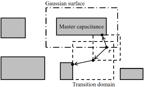
Figure 1: Two cases of random walk in the FRW algorithm for capacitance extraction (2-D view) [17].
After the procedure of FRW, the statistical mean of the weight values for the walks terminating at conductor j approximates mutual capacitance C between conductors i and j (if ij) or the self-capacitance C of master conductor i.
The iterative stopping condition of the FRW algorithm is primarily governed by predefined boundary conditions and a step limit. The boundary conditions are defined by expanding the region around the input layout. The algorithm performs random walks, and the iteration terminates once the path reaches the target boundary. Additionally, a step limit is enforced to prevent infinite iterations, ensuring the algorithm operates efficiently. The capacitance is then calculated based on these boundary conditions and step constraints.
III. ELECTROMAGNETIC ANALYSIS OF INTERCONNECT MODELS
In general, the rapid and accurate extraction of capacitance between interconnect conductors is challenging due to their arbitrary spatial positions and geometric shapes. When a potential difference exists between the interconnect conductors, the resulting charge distribution becomes uneven, leading to a non-uniform electric field distribution between the conductors (see Fig. 2).
In traditional CMOS structures, the two interconnect conductors i and j whose capacitance C needs to be evaluated are referred to as an interconnect pair (ICP). The substrate and other conductors are considered interference sources that can affect the electric field distribution of the ICP, leading to an overestimation or underestimation of the extracted capacitance. The closer the interference sources are to the ICP, the stronger their interference. When both the ICP and the substrate are present, the interference is less significant if there are projection overlapping regions within the ICP (see Fig. 3). However, if there are no projection overlapping regions within the ICP, the interference increases as the distance between conductor i and conductor j increases (see Figs. 4 and 5).
Figure 2: Electric field and potential distribution between two conductors.
Therefore, the presence of interference sources hinders the extraction of capacitance, resulting in prolonged capacitance extraction times.
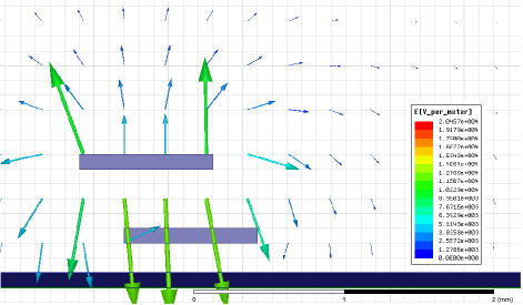
Figure 3: Electric field distribution between two near conductors with projection overlap region.
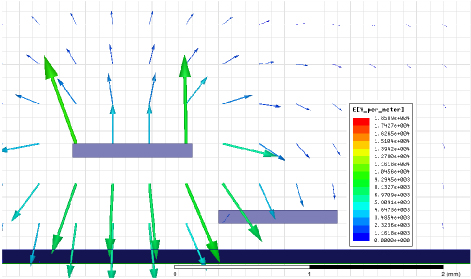
Figure 4: Electric field distribution between two near conductors without projection overlap region.
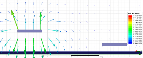
Figure 5: Electric field distribution between two distant conductors without projection overlap region.
IV. IMPROVED CAPACITANCE EXTRACTION METHOD
In the network structure of interconnect conductors, the conductor i whose total coupling capacitance needs to be extracted is referred to as the master conductor, while other conductors j (j i) are referred to as external conductors. Throughout the layout, some external conductors are in close proximity to the masterconductor, contributing significantly to the coupling capacitance C of the master conductor in its total coupling capacitance C. Conversely, some external conductors are further from the master conductor, and their coupling capacitance C contributes less to C. In methods such as solving the Laplace differential equation, BEM, and random walk methods, calculating the coupling capacitance between these distant external conductors and the master conductor consumes considerable memory and time without significantly improving the accuracy of C. Therefore, to enhance the solving speed, it is necessary to avoid calculating the coupling capacitance between these distant interconnect conductors and the master conductor while ensuring the accuracy of the total coupling capacitance. This approach is crucial for improving extraction speed and reducing memory consumption.
To minimize the number of other conductors that need to be considered when extracting the coupling capacitance of the master conductor, it is essential to comprehensively evaluate the effects of other conductors’ shapes, sizes, and relative positions on the master conductor’s coupling capacitance. Hence, we introduce the interconnect capacitance weight coefficient W, a variable used to calculate the proportion of the coupling capacitance C of an interconnect conductor in the master conductor’s total coupling capacitance C. To compute the weight coefficient W, we first determine whether there is an overlapping region between the master conductor and the external conductor and then apply the corresponding calculation method.
When there is a projection overlap region between the master and external conductors (see Fig. 3), we use the parallel plate capacitance model (see equation 3) to estimate a capacitance value as the weight coefficient W. In this case, the variable S in the model represents the area of the overlapping region, d is the dielectric thickness between the master and external conductors, and is the relative dielectric constant of the insulating layer between the conductors:
| (3) |
When there is no projection overlap region between the master and external conductors (see Figs. 4 and 5), we still use the parallel plate capacitance model to estimate the weight coefficient W. We connect the centers of the master and external conductors and generate a plane PA perpendicular to this line at its midpoint, projecting the master and external conductors onto plane PA as shown in Fig. 6. In this case, the variable S in the model represents the smaller projection area of the master and external conductors on plane PA, and d is the distance between the centers of the master and external conductors.
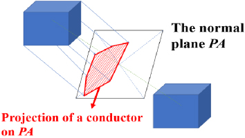
Figure 6: Projection of master and external conductors on normal plane PA for capacitance weight calculation.
After calculating the capacitance weight coefficient W for each external conductor relative to the master conductor, our goal is to use W to reduce the number of external conductors considered in field-solving methods while ensuring the estimation error of C remains within a specific range. To achieve this, we quickly extract the capacitance weight coefficients W of external conductors in the layout, compute the coupling capacitance weight coefficient W, and sort the external conductors in descending order based on W. Starting from the external conductor with the smallest W, we iteratively remove external conductors. After each removal, we record the removed capacitance weight coefficient W. We set an error threshold E. When the ratio of W to W exceeds E, we terminate the removal process.
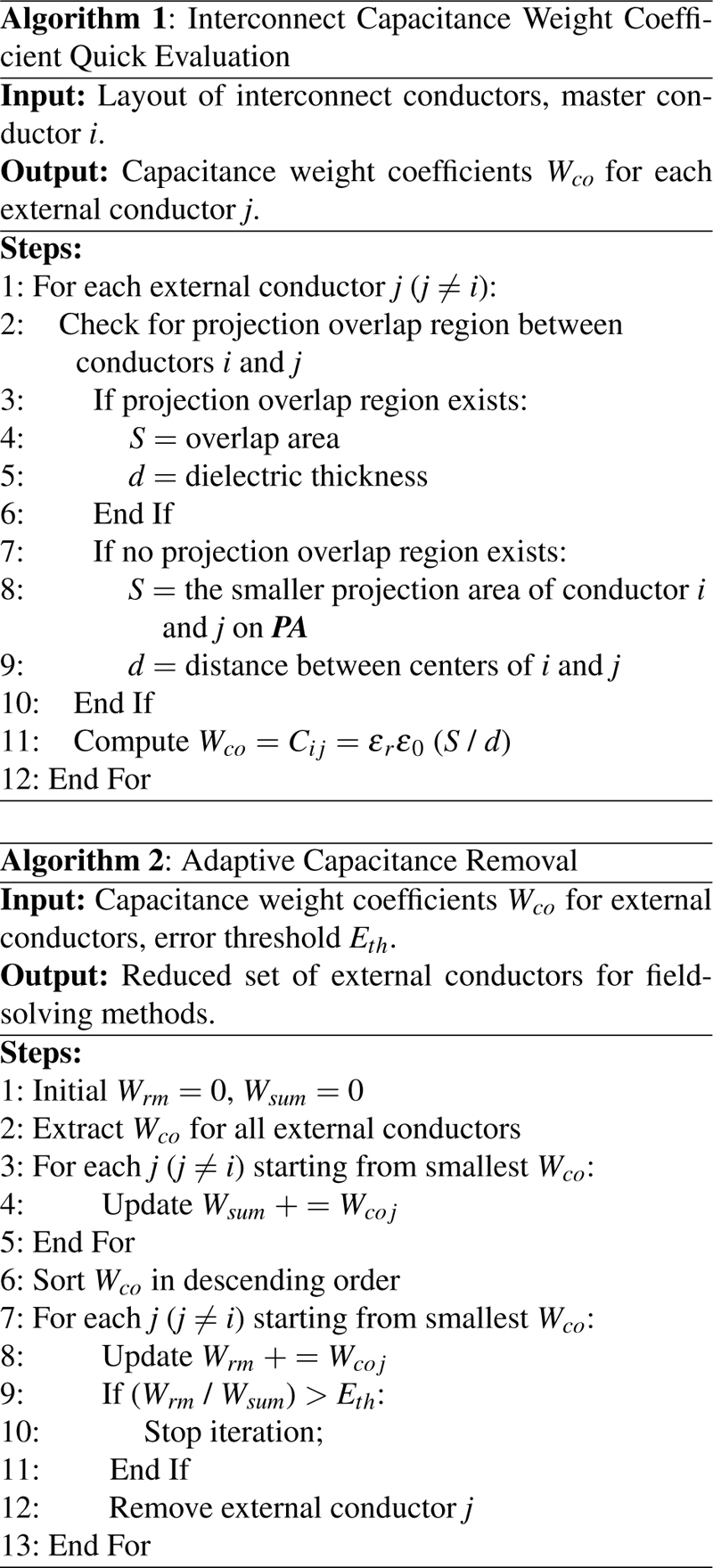
In summary, for the 3-D network structure of interconnect conductors, the improved capacitance extraction process is as follows. For the master conductor i we use the interconnect capacitance weight coefficient quick evaluation algorithm (Algorithm 1) to calculate the corresponding weight coefficients W for other external conductors j. Then, we use the adaptive capacitance removal algorithm (Algorithm 2) to reduce the number of external conductors considered in field-solving methods. Finally, we employ the field-solving method (FRW) for computation.
V. RESULTS
The test layout (called Sample 1) of the TSMC 65 nm process shown in Fig. 7, which includes 5991 conductors, is the sample layout for capacitance extraction, with the red-circled area indicating the master conductor for which the total coupling capacitance needs to be extracted. The experiments were conducted on a laptop with the following specifications: Intel Core i5-8300H CPU, 8 GB of RAM, and a 128 GB SSD. The operating system used was CentOS7, except for ANSYS Maxwell, which ran on Windows 10. In our work, although the actual scenario involves multiple dielectric materials, for the sake of computational simplicity, we have approximated the multi-dielectric environment as a single dielectric with an equivalent dielectric constant of 2.9 in the deployed FRW algorithm. This causes the FRW algorithm to have an error of less than 10% from the exact value. In our experimental setup, the boundary conditions of FRW algorithm were set to an expanded region that is 10 times the size of the input layout area. The maximum number of steps was fixed at 1000, with each step length restricted to 1 μm.
In general accuracy mode, using ANSYS Maxwell software, it takes 20 minutes to extract the coupling capacitance of the master conductor, yielding a capacitance value of 6.23 fF. However, after applying the improved capacitance extraction method to the FRW algorithm, we developed a more efficient field solver that adaptively balances time and extraction accuracy by setting an error threshold.
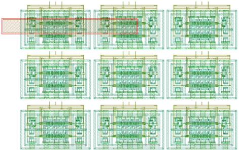
Figure 7: The layout for capacitance extraction (Sample 1).
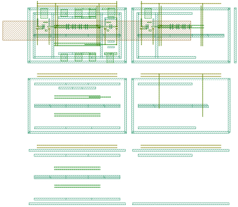
Figure 8: Simplified layout of conductors when E is 0.35.
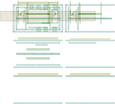
Figure 9: Simplified layout of conductors when E is 0.4.
When the error threshold is set to 0.35, the number of conductors in the layout decreases to 251 (see Fig. 8), resulting in a capacitance value of 5.79 fF. The extracted capacitance accuracy is maintained at over 92.9%, with a runtime of 13.66 seconds.
When the error threshold is set to 0.4, the number of conductors in the layout decreases to 167 (see Fig. 9), resulting in a capacitance value of 5.70 fF. The extracted capacitance accuracy is maintained at over 91.4%, with a runtime of 13.28 seconds.
When the error threshold is set to 0.4, the number of conductors in the layout decreases to 167 (see Fig. 9), resulting in a capacitance value of 5.70 fF. The extracted capacitance accuracy is maintained at over 91.4%, with a runtime of 13.28 seconds.
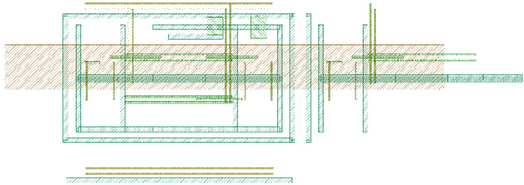
Figure 10: Simplified layout of conductors when E is 0.5.
Table 1: Capacitance extraction at different E values
| ErrorThreshold (E) | Number ofConductors | Total CouplingCapacitance Value | Capacitance Accuracy | ConductorRemoval Time | TotalRuntime | |
| Maxwell Data | / | 5991 | 6.23 fF | 100% | / | 20 min |
| Origin FRW Data | 0 | 5991 | 5.92 fF | 94.9% | / | 32.3 s |
| Improve FRW Data 1 |
0.35 | 251 | 5.79 fF | 92.9% | 0.271 s | 13.66 s |
| Improve FRW Data 2 |
0.4 | 167 | 5.70 fF | 91.4% | 0.280 s | 13.28 s |
| Improve FRW Data 3 |
0.5 | 68 | 5.43 fF | 87.1% | 0.296 s | 9.66 s |
When the error threshold is set to 0.5, the number of conductors in the layout decreases to 68 (see Fig. 10), resulting in a capacitance value of 5.43 fF. The extracted capacitance accuracy is maintained at over 87.1%, with a runtime of 9.66 seconds.
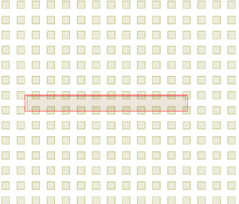
Figure 11: Layout for capacitance extraction (Sample 2).
Table 1 demonstrates the performance of the original FRW algorithm versus the improved method with conductor removal across different error thresholds (E). Despite the notable acceleration, which reduces the runtime from 32.3 seconds in the original FRW to just 9.66 seconds at E of 0.5, the time required for conductor removal remains minimal, ranging from 0.271 to 0.296 seconds. This demonstrates that the overhead introduced by conductor removal is negligible. Additionally, the method maintains high accuracy, with capacitance errors remaining within 10%, even at higher thresholds, ensuring a strong balance between computational speed and precision.
We have expanded our experiments by including two additional test cases (Sample 2 and Sample 3, shown in Figs. 11 and 12, respectively) to demonstrate the scalability and robustness of the proposed conductor removal method. The layout of Sample 2 contains 229 conductors, and the layout of Sample 3 contains 26 conductors, whereas the layout of Sample 1 consists of 5991 conductors. Figures 13 and 14 provide a clearer understanding of the impact of our algorithm on error and acceleration effects across different layout complexities.
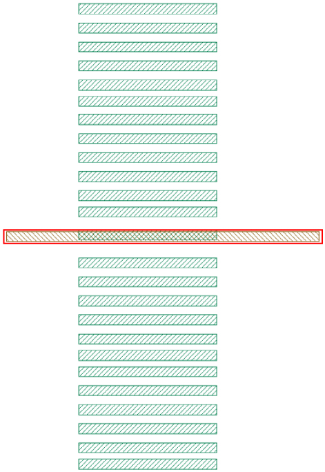
Figure 12: Layout for capacitance extraction (Sample 3).
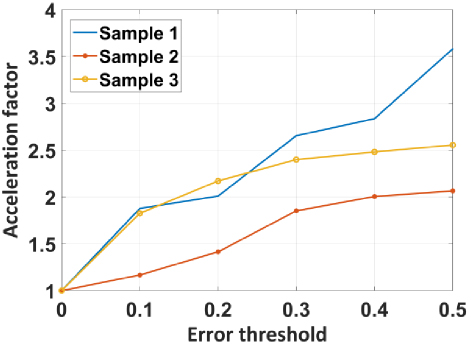
Figure 13: Impact of error threshold on relative capacitance error for different samples.
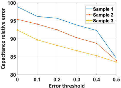
Figure 14: Impact of error threshold on acceleration factor for different samples.
Clearly, the performance of our algorithm is correlated with the complexity of the layout. The more complex the layout, the better the acceleration performance of our algorithm. However, a higher error threshold is likely to result in more significant capacitance extraction errors.
Experimental results demonstrate that by adjusting the error threshold in the improved capacitance extraction method applied to the FRW algorithm, a significant reduction in computation time can be achieved with only a minor loss in accuracy. In all three experimental samples, when E reached 0.5, a 2x acceleration was achieved compared to the scenario without conductor removal. This indicates that the improved method greatly enhances the efficiency of the capacitance extraction process while maintaining a high level of precision. The adaptive approach allows for a flexible trade-off between computational time and extraction accuracy, making it highly suitable for large-scale layout analysis where both factors are critical.
VI. CONCLUSION
This paper introduces an improved capacitance extraction method, proposing new concepts of capacitance weight coefficients and error thresholds. By removing conductors with low capacitance weight coefficients, the number of external conductors that need to be evaluated for extracting the capacitance of the master conductor is significantly reduced. The proposed improved capacitance extraction method can be applied to all field-solving methods and can adaptively balance accuracy and runtime while accelerating the process. In this paper, the FRW method is selected for combination with the proposed method to achieve faster runtime. This approach allows for high-accuracy and low-time assessments when evaluating interconnect delays. Experimental results show that, compared to the electromagnetic field simulation software ANSYS Maxwell, combining the improved capacitance extraction method with FRW achieves a 120x speedup with error control within 20%. Additional experimental cases demonstrate that our algorithm is highly suited for use in high-complexitylayouts.
In our research, we recognize that combining the conductor removal method with FEM/BEM-based approaches is certainly feasible and would broaden the applicability of our algorithm. By integrating the conductor removal technique, FEM can benefit from a reduced mesh volume or surface area, leading to smaller linear systems and improved computational efficiency, especially in large-scale 3-D models. Similarly, BEM would gain from a simplified boundary discretization process, as removing non-critical conductors would reduce the number of boundary points, thereby accelerating the solving process without compromising accuracy. These enhancements could extend the utility of our method in various scenarios, including FEM/BEM-based capacitance extraction. However, given the inherent advantages of the FRW algorithm—particularly its efficiency and scalability—we have chosen to focus on combining conductor removal with FRW in this study, as it aligns closely with the challenges we are addressing. Consequently, the simulation results in this paper specifically pertain to the integration of conductor removal with the FRW method.
ACKNOWLEDGMENT
This work was supported by Laboratory Specialized Scientific Research Projects of Beijing Smartchip Microelectronics Technology Co. Ltd.
REFERENCES
[1] S. Patidar and R. M. Bodade, “Evaluation trends and development in integrated circuit parasitic extraction,” in 2024 IEEE International Students’ Conference on Electrical, Electronics and Computer Science (SCEECS), Bhopal, India, pp. 1-7, 2024.
[2] D. Yang, W. Yu, Y. Guo, and W. Liang, “CNN-cap: Effective convolutional neural network based capacitance models for full-chip parasitic extraction,” in 2021 IEEE/ACM International Conference On Computer Aided Design (ICCAD), Munich, Germany, pp. 1-9, 2021.
[3] H. Q. Jin, Y. M. Wu, W. J. Wang, and H. J. Zhou, “Study on extraction of capacitance parameters of three dimensional interconnect structures based on finite element method,” in 2021 International Applied Computational Electromagnetics Society (ACES-China) Symposium, Chengdu, China, pp. 1-2, 2021.
[4] W. Yu and Z. Wang, “Organizing and storing of discretized BEM equations in 3D multi-dielectric parasitic capacitance extraction,” in ASICON 2001. 2001 4th International Conference on ASIC Proceedings, Shanghai, China, pp. 677-680, 2001.
[5] R. Ohnishi, D. Wu, T. Yamaguchi, and S. Ohnuki, “Numerical accuracy of finite-difference methods,” in 2018 International Symposium on Antennas and Propagation (ISAP), Busan, Korea, pp. 1-2, 2018.
[6] H. M. Yao, Y. W. Qin, and L. J. Jiang, “Machine learning based MoM (ML-MoM) for parasitic capacitance extractions,” in 2016 IEEE Electrical Design of Advanced Packaging and Systems (EDAPS), Honolulu, HI, pp. 171-173, 2016.
[7] W. Yu, H. Zhuang, C. Zhang, G. Hu, and Z. Liu, “RWCap: A floating random walk solver for 3-d capacitance extraction of very-large-scale integration interconnects,” IEEE Transactions on Computer-Aided Design of Integrated Circuits and Systems, vol. 32, no. 3, pp. 353-366, Mar. 2013.
[8] W. Yu, K. Zhai, H. Zhuang, and J. Chen, “Accelerated floating random walk algorithm for the electrostatic computation with 3-D rectilinear-shaped conductors,” Simul. Model. Pract. Theory, vol. 34, pp. 20-36, May 2013.
[9] C. Zhang and W. Yu, “Efficient space management techniques for large-scale interconnect capacitance extraction with floating random walks,” IEEE Trans. Comput.-Aided Design Integr. Circuits Syst., vol. 32, no. 10, pp. 1633-1637, Oct. 2013.
[10] C. Zhang and W. Yu, “Efficient techniques for the capacitance extraction of chip-scale VLSI interconnects using floating random walk algorithm,” in Proc. 19th Asia South Pac. Des. Autom. Conf. (ASP-DAC), pp. 756-761, 2014.
[11] C. Zhang, W. Yu, Q. Wang, and Y. Shi, “Fast random walk based capacitance extraction for the 3-D IC structures with cylindrical inter-tier-vias,” IEEE Trans. Comput.-Aided Design Integr. Circuits Syst., vol. 34, no. 12, pp. 1977-1990, Dec. 2015.
[12] W. Yu, Z. Xu, B. Li, and C. Zhuo, “Floating random walk-based capacitance simulation considering general floating metals,” IEEE Trans. Comput.-Aided Design Integr. Circuits Syst., vol. 37, no. 8, pp. 1711-1715, Aug. 2018.
[13] Z. Xu, C. Zhang, and W. Yu, “Floating random walk-based capacitance extraction for general non-Manhattan conductor structures,” IEEE Trans. Comput.-Aided Design Integr. Circuits Syst., vol. 36, no. 1, pp. 120-133, Jan. 2017.
[14] M. Visvardis, S. Stefanou, and E. Lourandakis, “Method of extracting capacitances of arbitrarily oriented 3D interconnects,” U.S. Patent 10,013,522, 3 July 2018.
[15] M. Visvardis, P. Liaskovitis, and E. Efstathiou, “Deep-learning-driven random walk method for capacitance extraction,” IEEE Transactions on Computer-Aided Design of Integrated Circuits and Systems, vol. 42, no. 8, pp. 2643-2656, Aug.2023.
[16] M. S. Abouelyazid, S. Hammouda, and Y. Ismail, “Accuracy-based hybrid parasitic capacitance extraction using rule-based, neural-networks, and field-solver methods,” IEEE Transactions on Computer-Aided Design of Integrated Circuits and Systems, vol. 41, no. 12, pp. 5681-5694, Dec. 2022.
[17] W. Yu, M. Song, and M. Yang, “Advancements and challenges on parasitic extraction for advanced process technologies,” in 2021 26th Asia and South Pacific Design Automation Conference (ASP-DAC), Tokyo, Japan, pp. 841-846, 2021.
BIOGRAPHIES

Dongyan Zhao received the B.S. degree and the M.S. degree in mechanical manufacturing from Shanghai Jiao Tong University in 1992 and 1998, respectively. Zhao is professor senior engineer, expert obtaining the special allowance of State Council, IEEE Senior member. Zhao is general manager of Beijing Smartchip Microelectronics Technology Co. Ltd, established the first chip R & D team in China’s power industry, built the largest industrial chip design enterprise in China. Zhao was duly elected a chief expert of State Grid Corporation of China in 2022.

Yanning Chen received the B.S. degree in computer science from Capital Normal University in 2002 and received the M.S. degree in electronic and communication engineering from Beijing University of Posts and Telecommunications in 2018. She is senior engineer, director of Research and Development center, Beijing Smartchip Microelectronics Technology Co. Ltd. She has significantly contributed to industrial chip reliability by addressing key technical challenges, developing technical standards, and establishing a quality assurance system for industrial chips.
Fang Liu received the Ph.D. degree from Tianjin University, Tianjin, China, in 2010. In 2015, she joined Beijing Smartchip Microelectronics Technology Co. Ltd., Beijing, China. Her current research interests include reliability of integrated circuits and semiconductor devices.
Yang Zhao Senior Engineer, manager of R&D Department of BeijingSmartchip Microelectronics Technology Co. Ltd. He has long beenengaged in the technical work ofindustrial chip testing and verification. He has more than 10 years of technical experience in the fields of IC-EMC, IC failure analysis and reliability. He is mainly responsible for the monitoring and analysis of the electric power field environment and the formulation of the related technical standards for the chips used in the electric power terminal. He has participated in the formulation /revision standard for more than 10 items, published six articles and 13 patents.

Yali Shao received the B.S. and M.S. degrees in electronic engineering from Zhejiang University, Hangzhou, China, in 2008 and 2011, respectively. She was in Texas Instruments from 2011 to 2017, and then in Analog Devices Inc. from 2017 to 2021. She current is in Beijing Smartchip Microelectronics Technology Co. Ltd. since 2021. Her research interests include analog IC design (Power IC, Driver IC, Isolation IC, and ADC IC), analog mixed-signal design and automation, process and device basic IP, such as OTP, IO, ESD, STD.
Dong Zhang received the B.S degree in applied physics from Lanzhou University of Technology, Lanzhou, China, in 2008. He then worked at RFMD (Beijing) where he was engaged in IC testing, reliability and failure analysis. In 2011, he joined Beijing Smartchip Microelectronics Technology Co. Ltd. and is responsible for analog IC automated design related work. His current research interests include analog circuit sizing and layout automation.
Yucheng Pan received his B.S. degree from Sun Yat-sen University, Guangdong, China, in 2022. He is currently a second-year graduate student at Sun Yat-sen University. His research interests include EDA technology for analog integrated circuits, with a particular focus on analog integrated circuit layout and routing.
Xiangyu Meng received the B.Sc. and Ph.D. degrees in electrical engineering from Tsinghua University, Beijing, China, in 2011 and 2017, respectively. From 2017 to 2018, he was a Post-Doctoral Fellow with the Electronic and Computer Engineering, Hong Kong University of Science and Technology, Hong Kong. He is currently an Associate Professor with the School of Electronics and Information Technology, Sun Yat-sen University, Guangzhou, China. His research interests include analog and RF IC design automation.
ACES JOURNAL, Vol. 39, No. 11, 970–979
doi: 10.13052/2024.ACES.J.391105
© 2024 River Publishers