Ultra Miniaturization and Transparency Frequency Selective Surface for Dual Band ISM Shielding
Dongming Guo and Huaxin Zhu
School of Science
Jiangnan University, Wuxi 214122, China
1422737299@qq.com, zhuhuaxin1312@163.com
Submitted On: May 28, 2024; Accepted On: August 27, 2024
ABSTRACT
This article presents an ultraminiaturized frequency selective surface (FSS) for shielding 2.4 GHz and 5.8 GHz (ISM) signals. The unit cell size is 0.056 0.056 ( is the free space wavelength at the first resonant frequency). It has smaller cell size and good transparency compared to previous ISM band studies, and transparency at 54%. The proposed FSS design consists of a wall structure and a compound square loop with 2.4 GHz and 5.8 GHz resonance frequencies for ISM band coverage. This FSS structure was fabricated on float glass with a dielectric constant of 8 by a photolithographic process. The fabricated FSS structure has excellent angular stability and polarization stability, which is further verified by experimentation. An easy optimization method is proposed to tune the independent resonant frequencies by optimizing the geometries individually. This FSS is interpreted by filtering through surface induced currents and equivalent circuit models. A prototype of the proposed FSS is fabricated and measured. The simulation results are in good agreement with the measured results. The proposed FSS has polarization insensitivity and 80 angle stability and is suitable for solving the EMI problem in ISM band.
Index Terms: frequency selective surface (FSS), ISM shielding, polarization stability, transparency, ultraminiaturized.
I. INTRODUCTION
With the rapid development of wireless communications, many unauthorized radios populate daily life, especially in the industrial, scientific and medical radio (2.4 GHz and 5.8 GHz ISM) bands. Interference in these frequency bands reduces communication performance and can even affect human health [1–8]. How to minimize interference and even protect your security in a complex wireless network environment is a critical issue. To solve this problem, indoor surfaces are usually converted to frequency selective surfaces (FSS) [9–15].
FSS consist of two dimensional planar or curved periodic arrays printed on dielectric substrates that exhibit frequency selection characteristics. FSS can effectively control the transmission and reflection of electromagnetic waves in order to screen electromagnetic waves of different frequencies [16]. Meanwhile, the filtering characteristics of FSS are affected by different geometry structures, dielectric substrates, and cell sizes. Based on the above characteristics, FSS is widely used in electromagnetic shielding [17], high impedance surfaces [18], radomes [19], and so on.
In recent years, miniaturized bandstop FSS for 2.4 GHz and 5.8 GHz have been widely studied. For example, a novel narrowband FSS hindering 2.4 GHz is mentioned in [20], achieving a narrower bandwidth and stable polarization response at 2.45 GHz by reducing the distance between the bottom legs and improving the three-legged periodic geometry. Reference [21] investigates the filtering properties of different geometries at 5.8 GHz, comparing the geometries of square, octagonal and hexagonal loops, and obtains a more stable FSS structure. However, but the above two FSS structures can only be used in a single frequency band, which is not able to satisfy the demand for dual-band in daily life. Furthermore, [22] used a double-layer convolution technique to obtain an FSS structure for shielding the 2.4 GHz and 5.8 GHz ISM bands with a miniaturization of 0.240.24. However, the double-layer structure increases the complexity of production. A miniaturized dual-bandstop FSS realized using geometrical nesting is proposed in [23]. The FSS structure consists of two complex geometries for hindering ISM bands. However, the angular stability of this FSS is 45, which has limitations for higher angle applications. None of the above FSS structures for shielding ISM signals have explored optical transparency. This is difficult to apply indoors, so an ultraminiaturized FSS with optical transparency is urgently needed.
In this paper, we design and fabricate a single layer, optically transparent FSS structure for shielding ISM bands. The proposed FSS has better miniaturization and good optical transparency compared to other studies, with FSS cell sizes up to 0.0560.056 and 54% transparency. In addition, the FSS structure has excellent polarization stability and large incidence angle stability. We also analyzed the surface induced currents of the proposed FSS and deduced the equivalent circuit model of the FSS. Finally, the prototype of this FSS was fabricated and measured in the field, and favorable reflections are obtained in all the desired frequency bands. Simulation and measurement results agree quite well.
II. STRUCTURE DESIGN
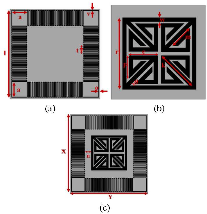
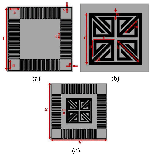
This paper proposes FSS printed on float glass [24] with a thickness of 1.6 mm and a dielectric constant of 8. It consists of a wall structure and a complex square loop. First step starts by designing the wall structure and the complex square loop in separate cells. The wall structure is an evolution of the square loop, and increases the effective electrical size by convolution, and makes it resonate at the first frequency and achieves miniaturization. The complex square loop is a modification of the square loop in order to achieve higher frequency resonance by adding four 45 diagonal arms to the square loop as well as eight triangular structures to optimize the internal geometry to a frequency slightly above 5.8 GHz. Finally, the two geometries are combined in the same cell to shield the ISM (2.4 GHz and 5.8 GHz) signals.
Figure 1: FSS geometries: (a) wall structure, (b) complex square loop, and (c) suggested dual-band FSS unit cell.
In addition, due to the mutual effect generated by stacking and nesting of the two structures, the distance between the two structures needs to be controlled to minimize interference, where the overall metal length and the operating frequency are in a specific relationship. FSS structures for individually shielded 2.4 GHz and 5.8 GHz are shown in Figs. 1 (a) and (b). Both structures are designed on a 77 mm cell. Figure 1 (c) shows the dual-bandstop characteristic FSS. Table 1 shows the parameters of the optimized FSS.
Table 1: The parameters of the optimized FSS
| Parameter | X | Y | n | l | a |
| Value (mm) | 7 | 7 | 0.1 | 6.92 | 1.44 |
| Parameter | v | t | o | r | w |
| Value (mm) | 0.04 | 0.12 | 0.04 | 3.8 | 0.2 |
| Parameter | p | e | k | m | |
| Value (mm) | 1.2 | 1.5 | 4.08 | 1.5 | 45 |
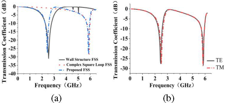
Figure 2 shows the frequency response curves of the three structures and the frequency response curves of TE and TM polarized vertical incidence. From Fig. 2 (a), we can observe that the wall structure has bandstop characteristic at 2.3-2.6 GHz (10 dB), which covers 2.4 GHz (WALN). The complex square loop has bandstop characteristic at 5.6-6 GHz (10 dB), which covers 5.8 GHz (ISM). The proposed FSS has two transmission zeros at 2.4 GHz and 5.8 GHz with transmission coefficients up to 28.3 dB and one transmission pole at 3.16 GHz. This confirms that two different resonators can be individually optimized to achieve the desired filtering characteristics. From Fig. 2 (b), it is observed that the two curves of TE polarization and TM polarization overlap, showing that the 90 rotation-symmetric design provides a polarization-insensitive response.
Figure 2: Simulated frequency response curve: (a) transmission coefficient for three structures and (b) TE and TM polarization for the proposed FSS.
III. SIMULATION ANALYSIS
A. Analysis of angular stability at different polarizations
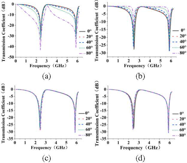
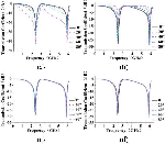
It is particularly important for the FSS structure to work stably at different polarization and incidence angles, thus Fig. 3 shows TE and TM wave polarization at different angles. From Fig. 3, it can be seen that the proposed FSS can provide a stable response to different and angles under TE and TM polarization waves without any significant change in transmission coefficients. The stability of the two polarizations is attributed to the compact periodic cell and symmetry of the periodic structure. Under TE polarization, the maximum frequency shift is 0.05 GHz (2%) at the first frequency and 0.01 GHz (0.17%) at the second frequency. Similarly, under TM polarization, the maximum frequency shift is 0.05 GHz (2%) at the first frequency and 0.049 GHz (0.8%) at the second frequency, which is due to the interactions that arise from the combination of two different structures. Interaction of the two different structures results in a weak shift of the resonance frequency.
Figure 3: Frequency curves for different polarizations and angles: (a) 0-80 angle TE polarization, (b) 0-80 angle TM polarization, (c) 0-80 angle TE polarization, and (d) 0-80 angle TM polarization.
In Figs. 3 (a) and (b), it can be seen that as the angle increases, the bandwidth of TE polarization increases and the bandwidth of TM polarization decreases. The wave impedance under TE polarization is and the angle change increases the wave impedance of TE polarization. Similarly, the wave impedance under TM polarization is , and the angle change decreases the wave impedance of TM polarization [25]. Wave impedance is directly proportional to the quality factor, and the relationship between the quality factor and the bandwidth is shown in the equation (1), which is the reason for the above mentioned change in bandwidth.
| (1) |
B. Analysis of current distribution and equivalent circuit
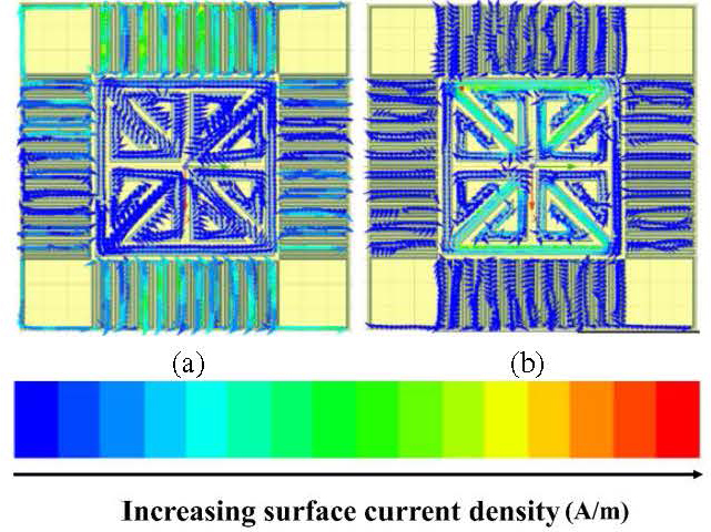
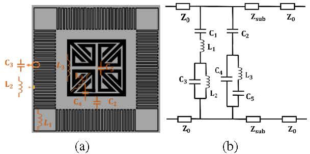
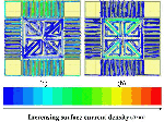
In order to have a deeper understanding of the working principle of FSS, the FSS current distribution as well as the equivalent circuit are further analyzed. Two transmission zeros at 2.4 GHz and 5.8 GHz are observed in Fig. 2 (b), and the vector current distribution at the two frequencies is shown in Fig. 4, where the colors and arrows denote the intensity and direction of the current, respectively. Figure 4 (a) shows the current distribution at frequency 2.4 GHz. The current flows in the walled structure and finally forms a closed loop, while there is little accumulation of current in the interior. Figure 4 (b) shows the current distribution at frequency 5.8 GHz. The current is mainly concentrated in the 45 diagonal arm as well as the square ring. It also proves that the two structures control the 2.4 GHz and 5.8 GHz ISM frequency bands, respectively. The equivalent circuit diagram of the FSS can be plotted from the current distribution graph and the complete equivalent circuit model is shown in Fig. 5.
Figure 4: FSS surface current distribution: (a) current distribution at frequency 2.4 GHz and (b) current distribution at frequency 5.8 GHz.
Figure 5: LC model visualization and simplified equivalent circuit model of the proposed FSS: (a) visualization of LC model and (b) simplified equivalent circuit model.
Based on the metal gap equivalent as capacitance and the metal dipole equivalent as inductance, Fig. 5 (a) shows the LC model visualization of the proposed FSS. In Fig. 5 (b), (= 377 ) is the wave impedance in free space and (= 134 ) is the wave impedance of the dielectric substrate, where . At 2.4 GHz, the current is concentrated on the wall structure. Current is more concentrated on , , and . The loop formed by these capacitive inductors exhibits low impedance, which leads to the mismatch of branch impedance. FSS exhibits band stopping characteristics, and the impedance of this FSS layer is . At 5.8 GHz, the reflection pattern of this FSS mainly involves a square loop, a 45 diagonal arm, and a triangular structure, so it is represented in the circuit by the series-parallel connection of , , and . The impedance of this FSS layer is []. The equivalent capacitance is mainly related to the gap and gap width of the periodic structure and the equivalent inductance value is related to the length and width of the periodic structure [26]. Equivalent circuit related equations are: , , , , , , , . M is the interaction between the two structures (M n), which is important for higher order resonance. An increase in the values of ‘a’ and ‘t’ parameters decreases the first resonant frequency (2.4 GHz). An increase in the values of ‘o’ and ‘v’ parameters increases the first resonant frequency. Similarly, an increase in the value of ‘r’ parameter decreases the second resonant frequency (5.8 GHz). An increase in the values of ‘w’ and ‘n’ parameters increases the second resonant frequency. A decrease in the value of ‘n’ parameter decreases the M value.
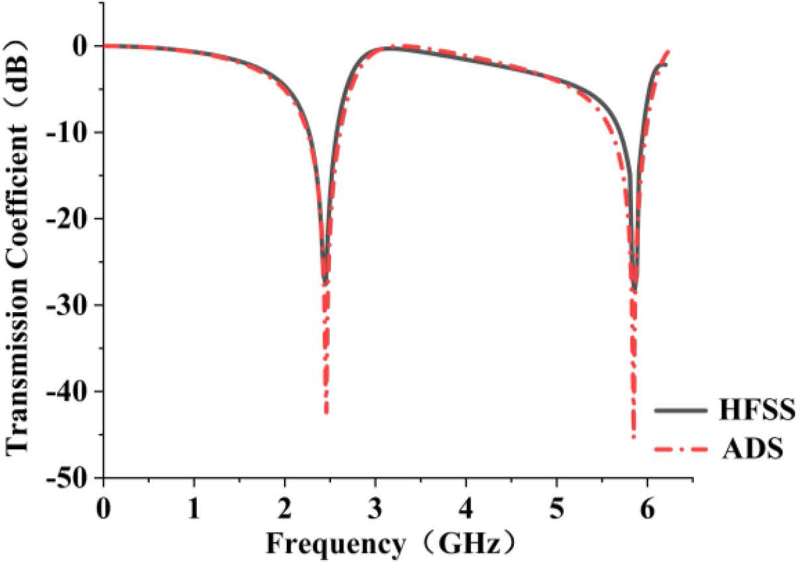
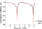
Figure 6: ADS software and HFSS software transmission coefficient.
In order to obtain the capacitance and inductance values of the equivalent circuit, we fitted capacitance and inductance in ADS by transmitting zeros, transmitting poles as well as bandwidths. Table 2 shows the optimized capacitance and inductance values of the fitted optimized counterparts as shown in Fig. 6, where we observed that the two models are very close to each other, thus verifying the reliability of the equivalent circuit model.
Table 2: Capacitive inductance values after fitting optimization
| Parameter | ||||
| Value (nH/pF) | 0.495 | 4.95 | 0.504 | 0.682 |
| Parameter | ||||
| Value (nH/pF) | 0.515 | 2.44 | 2.07 | 0.806 |
IV. EXPERIMENTAL VERIFICATION
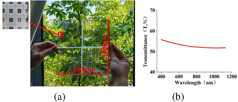
In the production of FSS prototypes, the float glass is first cleaned with alcohol. After a series of operations, such as spin-coating and drying, the float glass is placed inside the photolithography machine. The mask plate is placed on top of the photolithography machine, exposed using contact exposure, and finally dried and coated. The proposed FSS prototype is shown in Fig. 7 (a) A 9090 mm array of 1212 cells is printed on float glass by photolithography process, which has the advantages of high transmittance and low cost and can be perfectly suitable for indoor use. The photolithography process ensures the accuracy of the printed lines. The wall structure has an area of 11.6 mm, and the complex square structure has an area of 11.3 mm. With an optical transparency of 54%, leaves and trees can be seen clearly through the FSS, making it perfectly suited for indoor use.
Figure 7: Prototype and optical transmission spectra of the proposed FSS: (a) prototype of proposed FSS array and (b) optical transmission spectra of FSS.
Table 3: Comparison of the proposed FSS structure with previous miniaturized dual-band bandstop FSS studies
| REF | Operational Bands (GHz) | Transmission Coefficient (dB) | Bandwidths (MHz) | Polarization Insensitive | Angular Stability | Period of Unit Cell | (mm) | T% |
| [22] | 2.4 and 5.8 | 35 and 30 | 800 and 820 | NO | 60 | 0.24 | 125 | NO |
| [23] | 2.4 and 5.8 | 43 and 30 | 1100 and 700 | YES | 45 | 0.11 | 125 | NO |
| [27] | 2.4 and 5.8 | 37 and 20 | 900 and 400 | YES | 60 | 0.22 | 125 | NO |
| [28] | 2.4 and 5.8 | 27 and 28 | 902 and 928 | YES | 45 | 0.16 | 125 | NO |
| [29] | 2.4 and 5 | 49 and 50 | 550 and 400 | YES | 60 | 0.21 | 125 | NO |
| [30] | 2.4 and 5.4 | 45 and 43 | 300 and 500 | YES | 45 | 0.12 | 125 | 70 |
| [31] | 2.5 and 5.3 | 25 and 38 | 280 and 1770 | YES | 45 | 0.16 | 120 | NO |
| [32] | 9.8 and 10.7 | 30 and 41 | 330 and 373 | YES | 30 | 0.16 | 30.6 | NO |
| PFSS | 2.4 and 5.8 | 27 and 30 | 300 and 400 | YES | 80 | 0.056 | 125 | 54 |
A collimated light path is built on the experimental bench. The outgoing beam is irradiated on the FSS prototype, and a fiber optic spectrometer is used to receive the light beam that transmits through the FSS prototype. The transmittance curve is obtained in Morpho software. Figure 7 (b) shows the transmittance of the FSS prototype at 350-1200 nm. The fabricated FSS has a transmittance of 52% in most of the range, and the measured results are more in line with the calculated results.
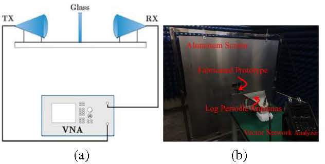
Figure 8 (a) shows the log periodic antennas model and Fig. 8 (b) shows the measurement setup. The measurement setup consists of BBHA 9120D log-periodic antenna and a FieldFox N9918A handheld vector network analyzer. In measuring the transmission plot, calibration was performed at 1-10 GHz frequency. Since the horn aperture is 2514 mm, four pieces of FSS prototypes were glued together with hot melt adhesive to cover the entire horn aperture and reduce diffraction. In order to improve the transmission efficiency of electromagnetic wave signals, an ordinary room is covered with wave absorbing cotton and the antenna speakers are placed at a calculated distance from each other. The sample is placed in the middle of the speakers during the measurement.
Figure 8: (a) Log periodic antennas model and (b) measurement setup.
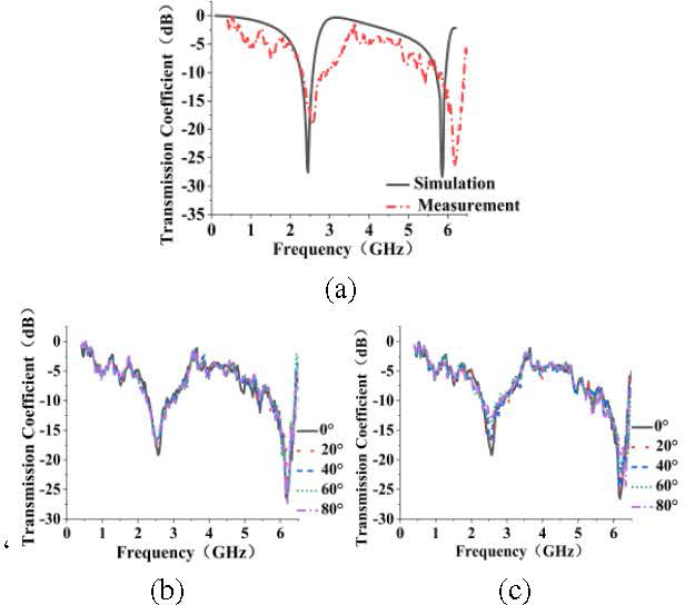
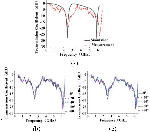
According to the measurement results in Fig. 9 (a), it can be seen that the measured resonant frequency has a slight offset. The offset at first frequency is 130 MHz, and the offset at second frequency is 250 MHz. The main reason for this offset is that the test room is not a complete microwave darkroom, as well as the error of debugging the vector network analyzer during the measurement process, so this is acceptable. The FSS prototype was measured for stability of different polarization angles, and the measurement results are shown in Figs. 9 (b) and (c). The prepared FSS has a stable frequency response in 0-80, and the resonance frequencies are more concentrated in 2.5 GHz and6.1 GHz.
Figure 9: Measured frequency response curve: (a) simulated and measured frequency response, (b) measurement curves of FSS at different incidence angles under TE polarization, and (c) measurement curves of FSS at different incidence angles under TM polarization.
To understand the advantages and disadvantages of the proposed FSS, information related to previous studies of miniaturized dual-band bandstop FSS is presented in Table 3, where “T” is the optical transparency, “” is the free-space wavelength at the first resonance frequency and “PFSS” is the proposed FSS.
We fabricated FSSs with smaller cell sizes. Some of the designs in Table 3 do not explore optical transparency nor polarization insensitivity, and most of the FSS structures have less angular stability than our designs. As can be seen in Table 3, our designed and printed FSS structures have single layer dual frequency operation, good transparency, ultraminiaturization, high level of polarization insensitivity and angular stability.
V. CONCLUSION
In this paper, an ultraminiaturized and optically transparent FSS structure is proposed to shield 2.4 GHz and 5.8 GHz (ISM signals). The proposed design has polarization insensitivity and high angular stability. Surface current analysis and collector circuit modeling are further presented. The resonant frequency of this FSS can be tuned by individual optimization of geometry. The FSS structure was prototyped using photolithography and then measured using a horn antenna and a vector network analyzer. Measurement results show that this FSS exhibits good transparency, and it shows stable frequency response under both TE and TM polarizations, and angular stability up to 80. Thus, the proposed FSS structure is an effective method to solve electromagnetic interference in the indoor ISM band.
ACKNOWLEDGMENT
This work was supported by the National Natural Science Foundation of China (61605067) and Open Fund of Key Laboratory of Optical System Advanced Manufacturing Technology, Chinese Academy of Sciences (KLOMT190103).
REFERENCES
[1] F. C. G. da Silva Segundo and A. L. P. S. Campos, “Compact frequency selective surface with dual-band response for WLAN applications,” Microw. Opt. Technol. Lett., vol. 57, pp. 265-268, 2015.
[2] S. Ahmed, F. A. Tahir, A. Shamim, and H. M. Cheema, “A compact Kapton-based inkjet-printed multiband antenna for flexible wireless devices,” IEEE Antennas Wireless Propag. Lett., vol. 14, pp. 1802-1805, 2015.
[3] S. Manokaran, R. Sivasamy, V. H. Muthukaruppan, and E. K. Roshan, “Design of polycarbonate-based dual-band conformal frequency-selective surface for 4G/5G shielding applications,” Microw. Opt. Technol. Lett., vol. 66, 2024.
[4] L. Tang, C. Wang, L. Yan, P. Gao, X. Zhao, and C. Liu, “Optically transparent and angularly stable broad-stopband frequency selective surface for millimeter wave electromagnetic interference mitigation,” Microw. Opt. Technol. Lett., vol. 66, 2024.
[5] S. M. Saeed, C. A. Balanis, and C. R. Birtcher, “Inkjet-printed flexible reconfigurable antenna for conformal WLAN/WiMAX wireless devices,” IEEE Antennas Wireless Propag. Lett., vol. 15, pp. 1979-1982, 2016.
[6] M. Ikram, M. S. Sharawi, and A. Shamim, “A novel very wideband integrated antenna system for 4G and 5G mm-wave applications,” Microw. Opt. Technol. Lett., vol. 59, no. 12, pp. 3082-3088, 2017.
[7] S. Balta and M. Kartal, “A novel double-layer low-profile multiband frequency selective surface for 4G mobile communication system,” Applied Computational Electromagnetics Society (ACES) Journal, vol. 37, pp. 420-427, 2022.
[8] Y. Li, P. Ren, Z. Xiang, B. Xu, and R. Chen, “Design of dual-stopband FSS with tightly spaced frequency response characteristics,” IEEE Microwave and Wireless Components Letters., vol. 32, pp. 1011-1014, 2022.
[9] M. Yan, S. Qu, J. Wang, J. Zhang, H. Zhou, H. Chen, and L. Zheng, “A miniaturized dual-band FSS with stable resonance frequencies of 2.4 GHz/5 GHz for WLAN applications,” IEEE Antennas Wirel. Propag. Lett., vol. 13, pp. 895-898, 2014.
[10] U. Farooq, M. F. Shafique, A. Iftikhar, and M. J. Mughal, “Polarization-insensitive triband FSS for RF shielding at normal and higher temperatures by retrofitting on ordinary glass windows,” IEEE Trans. Antennas Propag., vol. 71, pp. 3164-3171, 2023.
[11] M. Wang, L. Zhao, J. Wang, X. Liang, S. Zhang, Y. Li, and W. Yu, “A low-profile miniaturized frequency selective surface with insensitive polarization,” Applied Computational Electromagnetics Society (ACES) Journal, vol. 33, pp. 1003-1008, 2018.
[12] A. Meredov, K. Klionovski, and A. Shamim, “Screen-printed, flexible, parasitic beam-switching millimeter-wave antenna array for wearable applications,” IEEE Open J. Antennas Propag., vol. 1, pp. 2-10, 2020.
[13] M. Idrees, Y. He, S. Ullah, and S. Wong, “A dual-band polarization-insensitive frequency selective surface for electromagnetic shielding applications,” Sensors, vol. 24, 3333, 2024.
[14] K. Klionovski, M. S. Sharawi, and A. Shamim, “A dual-polarization switched beam patch antenna array for millimeter-wave applications,” IEEE Trans. Antennas Propag., vol. 67, no. 5, pp. 3510-3515, 2019.
[15] R. Natarajan, M. Kanagasabai, S. Baisakhiya, R. Sivasamy, S. Palaniswamy, and J. K. Pakkathillam, “A compact frequency selective surface with stable response for WLAN applications,” IEEE Antennas Wirel. Propag. Lett., vol. 12, pp. 718-720, 2013.
[16] J. C. Vardaxoglou, Frequency Selective Surfaces: Analysis and Design. New York: Research Studies Press, 1997.
[17] M. Bashiri, C. Ghobadi, J. Nourinia, and M. Majidzadeh, “WiMAX, WLAN, and X-band filtering mechanism: Simple-structured triple-band frequency selective surface,” IEEE Antennas Wireless Propag. Lett., vol. 16, pp. 3245-3248,2017.
[18] P. Deo, A. Methta, D. Mirshekar Syahkal, P. J. Massey, and H. Nakano, “High impedance surface-based square loop antenna with rf-absorber,” Microw. Opt. Technol. Lett., vol. 53, pp. 481-485, 2011.
[19] H. Ahmad, M. Rahman, S. Bashir, W. Zaman, and F. C. Seman, “Miniaturized frequency selective radome operating in the X-band with wideband absorption,” Applied Computational Electromagnetics Society (ACES) Journal, vol. 34, pp. 1915-1921, 2019.
[20] M. Kartal, S. K. Pinar, B. Doken, and I. Gungor, “A new narrow band frequency selective surface geometry design at the unlicensed 2.4-GHz ISM band,” Microw. Opt. Technol. Lett., vol. 55, pp. 2986-2990, 2013.
[21] T. Hong, Y. Lee, F. Wee, Y. You, M. N. A. Karim, N. H. Ramli, H. Gan, and M. A. Jamlos, “Study of 5.8 GHz band-stop frequency selective surface (FSS),” International Journal of Integrated Engineering, vol. 11, pp. 244-251, 2019.
[22] B. Döken and M. Kartal, “Dual layer convoluted frequency selective surface design in the 2.4 and 5.8 GHz ISM bands,” Applied Computational Electromagnetics Society (ACES) Journal, vol. 33, pp. 413-418, 2018.
[23] B. Döken and M. Kartal, “Dual-band frequency surface design by implementing a simple design technique,” IETE J Res., vol. 68, pp. 2049-2054, 2019.
[24] Float Glass – Properties and Applications [Online]. Available: https://www.azom.com/properties.aspx?ArticleID=89.
[25] P. Wei, C. Chiu, and T. Wu, “Design and analysis of an ultraminiaturized frequency selective surface with two arbitrary stopbands,” IEEE Transactions on Electromagnetic Compatibility, vol. 61, pp. 1447-1456, 2019.
[26] T. Liu and S. S. Kim, “Design of wide-bandwidth electromagnetic wave absorbers using the inductance and capacitance of a square loop-frequency selective surface calculated from an equivalent circuit model,” Opt. Commun., vol. 359, pp. 372-377, 2016.
[27] B. Döken and M. Kartal, “Easily optimizable dual-band frequency selective surface design,” IEEE Antennas Wirel. Propag. Lett., vol. 16, pp. 2979-2982, 2017.
[28] V. F. Barros, S. Segundo, A. L. P. Campos, S. G. da Silva, and A. Gomes Neto, “A novel simple convoluted geometry to design frequency selective surfaces for applications at ISM and UNII bands,” J Microw. Optoelectron. Electromagn. Appl., vol. 16, pp. 553-563, 2017.
[29] M. A. Hussaini, M. I. Sulaiman, G. I. Kiani, and J. Khan, “Frequency selective window blinds for indoor WLAN shielding,” Microw. Opt. Technol. Lett., vol. 66, issue 1, 2024.
[30] U. Farooq, A. Iftikhar, A. I. Najam, S. A. Khan, and M. F. Shafique, “An optically transparent dual-band frequency selective surface for polarization independent RF shielding,” Optics Communications, vol. 546, 2023.
[31] R. V. D. Lira, B. S. da Silva, A. L. P. S. Campos, and A. G. Neto, “A dual-band complementary frequency selective surface combining structures that provides narrow and wide stop-band frequency responses,” Microw. Opt. Technol. Lett., vol. 65, pp. 3107-3112, 2023.
[32] T. Qin, C. Huang, Y. Cai, and X. Lin, “Dual-band frequency selective surface with different polarization selectivity for wireless communication application,” Sensors, vol. 23, no. 9, p. 4264, 2023.
BIOGRAPHIES

Dongming Guo was born in QuanZhou, Fujian, China, in 2000. He received the B.S. degree from the Xiamen University of Technology, Xiamen, China, in 2022. Currently, he is focusing on antenna and microwave devices.

Huaxin Zhu received his Ph.D. degree in 2011. Since 2011, he has worked on optical thin film design, preparation and frequency selective surfaces. Currently, he is an Associate Professor in the Jiangnan University, School of Science.
ACES JOURNAL, Vol. 39, No. 6, 520–526
doi: 10.13052/2024.ACES.J.390605
© 2024 River Publishers
