Design of a High-frequency Antenna Along a Conducting Surface
Marius H. Vogel and Mark H. Smith
1Georgia Tech Research Institute
Williamsburg, VA 23185, USA
marius.vogel@gtri.gatech.edu
2Georgia Tech Research Institute
Smyrna, GA 30080, USA
mark.smith@gtri.gatech.edu
Submitted On: July 20, 2024; Accepted On: October 7, 2024
ABSTRACT
Antennas in the high-frequency (HF) band (3-30 MHz) tend to be large and almost always protrude from the structure on which they are mounted. This paper will present a design in which the antenna is installed parallel to and close to a conducting surface. To achieve a small mismatch loss, a thin high-impedance metamaterial surface was designed. The bandwidth is enlarged by applying non-Foster impedances between the ends of the antenna arms and the conducting surface.
Index Terms: Artificial magnetic conductor, broad band, HF antenna, impedance matching, low profile.
I. INTRODUCTION
The high-frequency (HF) band is attractive for over-the-horizon communication and sensing, due to the reflective properties of the ionosphere at those frequencies. This is especially the case for frequencies in the lower half of the band. Due to the wavelengths involved, e.g., 30 m at 10 MHz, HF antennas tend to be large, and almost always protrude from the structure on which they are mounted. It can be advantageous to integrate the HF antenna with a structure, e.g. for reasons of aerodynamics, detectability or esthetics. For instance, a large unmanned aerial system may require an HF antenna that does not deteriorate its aerodynamics and does not increase its radar signature. However, when an HF antenna is mounted both parallel and close to a conducting surface, the mismatch loss will be large.
The solution presented in this paper makes use of a high-impedance surface. A regular conducting surface has a low impedance, enabling electrons in the surface to react quickly to fields produced by the antenna. This reduces the radiation by orders of magnitude. A high-impedance surface prevents electrons from reacting this way. It can be designed without changing the underlying conducting surface.
The concept of high-impedance surfaces was pioneered by Sievenpiper et al. [1, 2, 3, 4] in the late 1990s. The authors explain how the metamaterial surface, which is a conducting surface, does not conduct AC currents or surface waves within a forbidden band, and reflects normal-incidence electromagnetic waves with no phase reversal. The authors show how antennas can be mounted parallel to and close to such a surface without suffering a large mismatch loss. More examples are presented by Best and Hanna [5].
Subsequent researchers have designed many high-impedance surfaces with improved properties, such as compact or broadband designs [6, 7, 8]. All these designs exhibit their special properties at microwave frequencies. To the authors’ knowledge, no high-impedance surfaces have yet been designed to operate at MHz frequencies, in the HF band.
The design presented here was inspired by [7], but modified significantly to work in the HF band while being thin. With this high-impedance surface, the HF antenna has a small mismatch loss in a 2% bandwidth.
The next challenge is to increase the bandwidth. Visser [9] presents a folded dipole antenna above a high-impedance surface and exploits the fact that a folded dipole offers more degrees of freedom for optimization than an ordinary dipole antenna. The HF antenna presented in this article also takes advantage of additional degrees of freedom offered by a folded dipole, albeit in a different way. In this case, the ground takes the place of the long wire of the folded dipole. The ends of the dipole arms connect to the ground plane. We use the additional design freedom offered by the connections to load the ends of the antenna with an imaginary-valued non-Foster impedance. Sussman-Fort and Rudish [10] explore ways to realize such impedances. With proper loads, the bandwidth can be increased from 2% to 30%.
II. HIGH-IMPEDANCE SURFACE DESIGN AND RESULTS
As mentioned, the design presented here was inspired by [7]. However, it was not accomplished by taking an existing microwave design and multiplying the dimensions by two orders of magnitude. The value of a high-impedance surface lies in the fact that it is thin. As will be specified below, our antenna is only 3 cm above the surface, which itself has a thickness of 1 cm. The total thickness of 4 cm is only one thousandth of a wavelength at 7.5 MHz. By comparison, the HF antenna “with extremely low profile” reported in [11] has a rather high profile: it is one meter above its ground plane.
The design process starts by the selection of a suitable geometry concept. Metamaterial surfaces exist in many forms, e.g. coupled patches on one dielectric layer, overlapping patches on multiple layers, with or without vias to the underlying conducting plane. In this case, we have chosen a periodic structure of spirals on one layer, without vias. For a unit cell, geometry and material variables are adjusted to optimize the reflection phase of an incident plane wave at the desired operating frequency. A low-impedance surface imposes the boundary condition that the total tangential electric field be close to zero, which causes the reflection phase to be close to 180 degrees. The surface will be a high-impedance surface to incoming plane waves when the reflection phase is close to zero degrees.
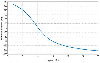
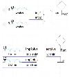
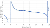
The design shown in Fig. 1 accomplishes this by using a ferrite material with 400; 1. The thickness is only 10 mm. The unit-cell size is 0.30.3 m. The metal trace width is 24 mm and the gap width equals 6 mm. The reflection phase as a function of frequency is shown in Fig. 2. Note that the phase equals zero at 10 MHz, and the 90 bandwidth ranges from 6.77 to 14.95 MHz, which is a bandwidth of about 65%.
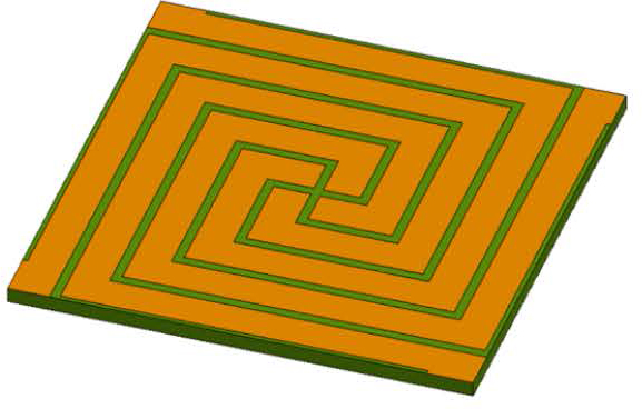
Figure 1: High-impedance surface unit cell.
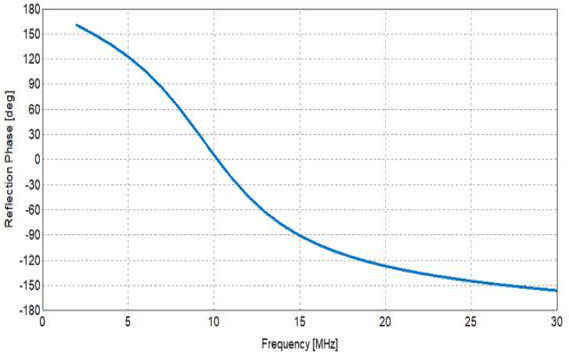
Figure 2: Reflection phase of a normally-incident plane wave on the high-impedance surface.
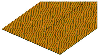
The actual high-impedance surface was constructed as a 535 array of unit cells, a small part of which is shown in Fig. 3.
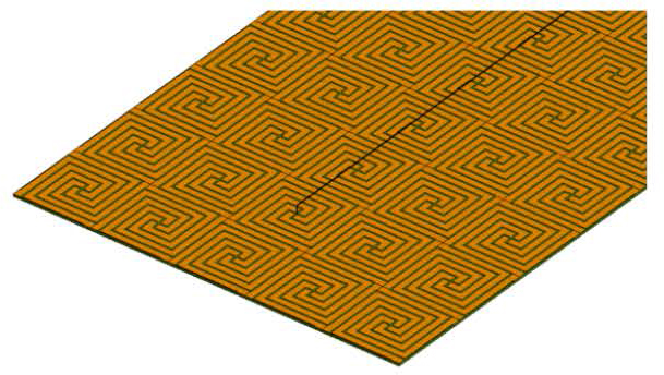
Figure 3: Part of the high-impedance surface with the antenna.
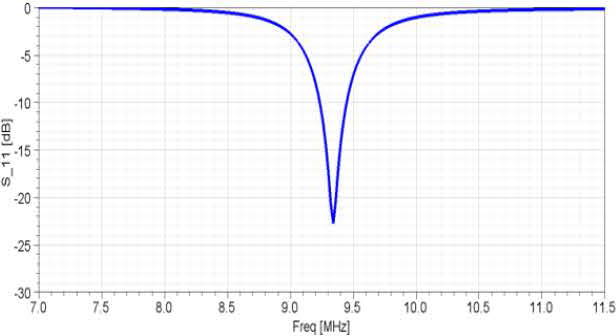
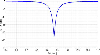
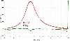
Figure 4: Reflection coefficient of the dipole with electrically shorted arms over the high-impedance surface.
With this high-impedance surface, the HF antenna has a small mismatch loss in a 2% bandwidth. This is much less than the bandwidth suggested in Fig. 2, but that was for an incoming plane wave. With an antenna close to the surface, the fields are quite different from a plane wave, to the extent that our design approach was not guaranteed to work. The antenna is mounted 30 mm above the structure; this is one-thousandth of a wavelength at 10 MHz. The antenna arms are metal traces with a width of 4 mm. The ends of the arms are connected to the ground plane by metal strips that pass through a gap between spirals without touching the spirals. The return loss is shown in Fig. 4 for a source impedance of 50 .
III. COMPUTATIONAL METHODS
For the 3D simulations of the antenna and the high-impedance surface, the Finite Element Method was used, as implemented in Ansys HFSS, part of Ansys Electronics Desktop [12]. Two advantages of this Finite-Element implementation stand out: automatic adaptive mesh refinement and hierarchical basis functions. Thanks to these, it was possible to run the simulation on one computer with a memory capacity of 128 GB. The automatic adaptive mesh refinement ensures that the final mesh is fine enough where needed, while it remains coarser where this is possible. The hierarchical basis functions enable an iterative solution in which a solution with zero-order basis functions serves as an initial guess for an iterative solution with first-order basis functions.
The computational domain was a cylindrical air volume around the structure, with the antenna close to the cylinder axis, and a radius of 10 m, which corresponds to a quarter wavelength at 7.5 MHz. The air volume was terminated by an Absorbing Boundary Condition. Although more-advanced techniques such as Perfectly Matched Layers and the Finite-Element Boundary-Integral method could be used to reduce the size of the air volume, this was not necessary in this case because the volume in terms of cubic wavelengths was modest. The motivation for a cylindrical volume was that radiated fields would meet the boundary at angles almost normal to their propagation direction. Absorbing boundary conditions are most effective at those angles.
The peak memory requirement was 109 GB for a Finite-Element matrix equation with 33 million unknowns. The maximum CPU time for one frequency sample was 2 hours 13 minutes. Thanks to parallel processing on 16 cores, the maximum elapsed wall-clock time for one frequency sample was 24 minutes and 14 seconds. A discrete frequency sweep, e.g. from 5 to 12 MHz, typically consisted of 71 samples.
IV. NON-FOSTER LOAD DETERMINATION AND RESULTS
Figure 5 shows the input impedance Z of the design of the previous section. Note that the real part of Z is not far from 50 over an appreciable bandwidth while the imaginary part of Z varies much more with frequency. Therefore, we will interrupt the short circuits at the ends of the antenna arms and insert imaginary-valued impedances, such that the imaginary part of the antenna input impedance be close to zero over a large band.
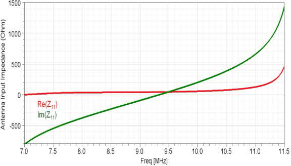
Figure 5: Real and imaginary parts of antenna input impedance as a function of frequency.
Long and Sievenpiper have explored the use of non-Foster circuits in relation with high-impedances surfaces [13], but they loaded the periodic surface features rather than the antenna. They have managed to bring the operating frequency of an antenna with a thin high-impedance surface down to the UHF band, and explain why achieving such a design is a challenge. This underscores that achieving the same in the HF band (an order of magnitude lower) is exceptional.
The most efficient workflow to determine the aforementioned impedances at the ends of the antenna arms involves rapid optimization in a circuit simulator. First, in the 3D electromagnetic simulation model, ports were placed in the locations where the impedances would be inserted later, between the ends of the antenna arms and the ground plane. Together with the feed port already present, this resulted in a three-port device. Frequency-dependent S-matrices were determined with a 3D full-wave simulation. Figure 6 shows how the S-parameter representation of the model was used in the circuit simulator in the Ansys Electronics Desktop, where a source and passive electric components were connected to the S-parameter block.
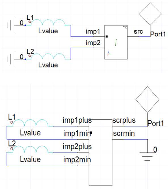
Figure 6: Two equivalent implementations of the HFSS three-port device (rectangular symbol) as part of the circuit, with impedances to be optimized.
Figure 6 shows two equivalent implementations, both featuring the same three-port HFSS model. The top schematic has one pin per port; the bottom schematic has two pins per port. Behind the scenes, the S-parameter block contains all necessary information. In the schematic with one pin per port, the use of multiple ground symbols may seem non-intuitive, as this could enforce, in some circuit simulators, an unphysical zero-L, zero_R connection between two distance locations in the 3D structure. In the Ansys Electronics Desktop, the ground symbol merely indicates a connection to the second terminal on the same port. This has been verified with the bottom schematic, in which the connections to the second terminal on each port have been made explicit.
In the circuit simulator, simulations take only a fraction of a second. Thus, the desired impedance values could be determined rapidly.
These impedance values, which are imaginary-valued, are shown in Fig. 7. They are non-Foster impedances that follow a smooth curve with a negative slope between 5.9 and 11.8 MHz. The behavior near 8 MHz might be related to the effective electrical length of the spirals on the ferrite substrate. How to realize these impedances is still a topic of research, about which Sussman-Fort and Rudish [10] as well as Long and Sievenpiper [13] offer valuable information.
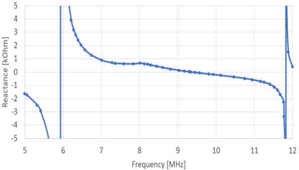
Figure 7: Reactance values at the ends of the antenna arms required to negate the imaginary value of antenna input impedance.
Figure 8 shows the resulting antenna input impedance Z when these non-Foster impedances are added. Note that the modification brought the imaginary part of Z to zero, as intended, but has affected the real part of Z.
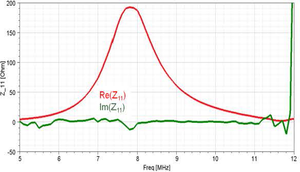
Figure 8: Antenna input impedance after adding the impedances of Fig. 7 between the ends of the antenna arms and the ground plane.
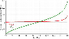
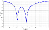
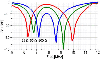
The resulting return loss S depends on the source impedance. Figure 9 shows the return loss when the source impedance equals 100 . Note that the -10 dB bandwidth is almost 30%.
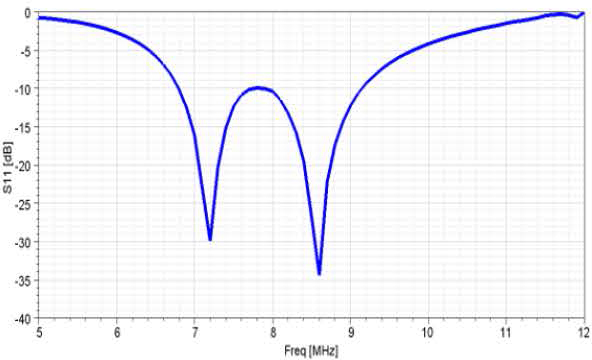
Figure 9: Reflection coefficient when the source impedance equals 100 .
Furthermore, operating frequencies outside this band are easily reached with different source impedances. With a 50 source impedance, the minima move about 1 MHz farther apart, enabling operation at lower and higher frequencies, while S reaches a local maximum of -5 dB between those frequencies. With a 25 source impedance, this trend continues. Figure 10 shows the return loss for the three source impedances. Note that the lower and upper operating bands offer generous -10 dB bandwidths of 13-14%.
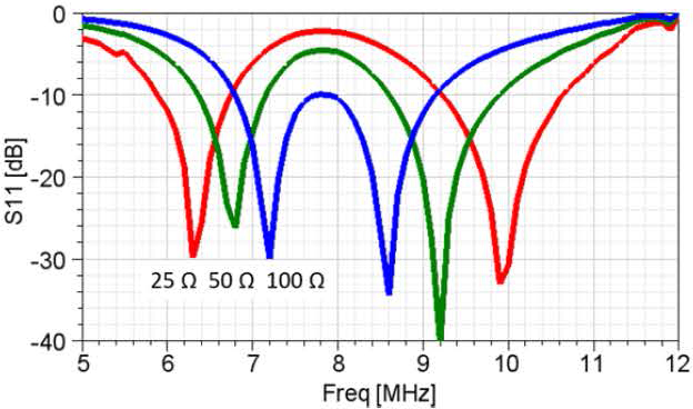
Figure 10: Return loss with various source impedances, which makes lower and higher frequencies easily attainable.
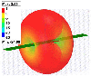
Finally, Fig. 11 shows the antenna pattern at 9.3 MHz. Since the high-impedance surface is narrow relative to the wavelength, the antenna pattern is similar to that of the dipole antenna. However, due to the connections at the ends of the arms, the peak gain is slightly higher than that of a dipole antenna.
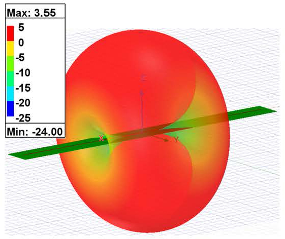
Figure 11: Gain [dBi] of the antenna with high-impedance surface.
V. CONCLUSION
An HF antenna has been made to operate when mounted parallel and close to a conducting surface. This was achieved with a thin high-impedance metamaterial surface. To the authors’ knowledge, such a structure had not yet been designed for HF antennas. The bandwidth was enhanced by adding imaginary-valued impedances between the ends of the antenna arms and the conducting surface. The design of these non-Foster impedances is still a topic of research.
REFERENCES
[1] D. Sievenpiper, L. Zhang, and E. Yablonovitch, “High-impedance electromagnetic ground planes,” in IEEE MTT-S Int. Microwave Symp. Dig., Anaheim, CA, vol. 4, pp. 1529-1532, June 1999.
[2] D. Sievenpiper, Lijun Zhang, R. F. J. Broas, N. G. Alexopolous, and E. Yablonovitch, “High-impedance electromagnetic surfaces with a forbidden frequency band,” IEEE Trans. Microwave Theory Tech., vol. 47, no. 11, pp. 2059-2074, Nov. 1999.
[3] D. Sievenpiper, R. Broas, and E. Yablonovitch, “Antennas on high-impedance ground planes,” in 1999 IEEE MTT-S Int. Microwave Symp. Dig., Anaheim, CA, vol. 3, pp. 1245-1248, June 1999.
[4] R. F. J. Broas, D. F. Sievenpiper, and E. Yablonovitch, “A high-impedance ground plane applied to a cellphone handset geometry,” IEEE Trans. Microwave Theory Tech., vol. 49, no. 7, pp. 1262-1265, July 2001.
[5] S. R. Best and D. L. Hanna, “Design of a broadband dipole in close proximity to an EBG ground plane,” IEEE Antennas and Propagation Magazine, vol. 50, no. 6, pp. 52-64, Dec. 2008.
[6] S. Raza, M. A. Antoniades, and G. V. Eleftheriades, “A compact low-profile high-impedance surface for use as an antenna ground plane,” in IEEE Int. Symp. Antennas and Propagation (APSURSI), Spokane, WA, pp. 1832-1835, July 2011.
[7] A. Bellion and M. Cable, “A new wideband and compact High Impedance Surface,” in 15 Int. Symp. Antenna Tech. and Applied Electromagnetics (ANTEM), Toulouse, France, pp. 1-5, June 2012.
[8] H. Mirshahram and W. Qun, “Meander line-based high impedance surface with high angular stability of resonant frequency,” in 3rd IEEE Int. Symp. Microwave, Antenna, Propagation and EMC Technologies for Wireless Communications, Beijing, China, pp. 1246-1249, Oct. 2009.
[9] H. J. Visser, “Printed folded dipole antenna design for rectenna and RFID applications,” in 7th European Conference on Antennas and Propagation (EuCAP), Gothenburg, Sweden, pp. 2852-2855, Apr. 2013.
[10] S.E. Sussman-Fort and R.M. Rudish, “Non-Foster impedance matching of electrically-small antennas,” IEEE Trans. on Antennas Propagat., vol. 57, no. 8, pp. 2230-2241, Aug. 2009.
[11] W. Lin and Z. Shen, “Broadband horizontally polarized HF antenna with extremely low profile above conducting ground,” in 2013 IEEE Antennas and Propagation Society International Symposium (APSURSI), Orlando, FL, pp. 688-689, July 2013.
[12] Ansys Electronics Desktop, version 2024 R1, ANSYS, Canonsburg, PA, 2024.
[13] J. Long and D. F. Sievenpiper, “Low-profile and low-dispersion artificial impedance surface in the UHF band based on non-Foster circuit loading,” in IEEE Trans. on Antennas Propagat., vol. 64, no. 7, pp. 3003-3010, July 2016.
BIOGRAPHIES

Marius (Martin) H. Vogel obtained his M.Sc. in Physics at Leiden University in the Netherlands, and worked at TNO Defense and Security, a Dutch defense contractor. Due to the nature of the research, he obtained a Ph.D. in electromagnetics from Delft University of Technology at that time. A one-year assignment on directed-energy weapons at the US Air Force Lab in Albuquerque, NM brought him to the USA.
He has worked at Ansoft/ANSYS, and later at Altair Engineering, both in the USA, in various roles on a wide variety of applications in high-frequency electromagnetics, propagation and communication. Applications include antenna design, antenna placement, radar cross section, electromagnetic interference, bio-electromagnetics, signal integrity and more. Martin joined GTRI in April 2023 and is based in the Hampton Roads area in Virginia.

Mark H. Smith has over 40 years of experience in RF, microwave, and optical technology and applications, with over 30 years of experience at GTRI conducting and directing research, concept development, analysis, computer modeling, capability development, and testing, with a primary focus on technology and systems for RF sensing and Electronic Warfare. He has been Chief Scientist of GTRI’s Sensors and Electromagnetic Applications Laboratory (SEAL) since 2012. Dr. Smith received his Ph.D. from Georgia Institute of Technology (GA Tech) in 2002, an M.S. from GA Tech in 1987, and a B.E.E. With Highest Honor from GA Tech in 1982.
ACES JOURNAL, Vol. 39, No. 8, 727–732
doi: 10.13052/2024.ACES.J.390808
© 2024 River Publishers