Compact Single and Dual-Band Branch-Line Coupler with Effective Fractional Bandwidth for Wireless Communication Systems
G. Srividhya and S. Maheswari
Department of ECE
Panimalar Engineering College, Poonamallee, Chennai, Tamil Nadu 600123, India
srividhyakrishiv@gmail.com, maheswarisp@yahoo.co.in
Submitted On: September 3, 2024; Accepted On: May 22, 2025
ABSTRACT
Multiple wireless communication systems make use of a branch-line coupler (BLC), which is a passive microwave component. For the purpose of splitting and combining microwave signals, as well as providing a 90-degree phase shift between the output ports, this 4-port device is made from four quarter-wavelength (/4) transmission lines. Having recently developed a dual-band branch-line coupler (DBBLC), there has been a lot of attention paid to this development. When it comes to getting dual-band (DB) functioning of a BLC, one of the most common approaches is stub loaded transmission lines. For the BLC, stubs may be positioned either in the center of the arms or at the input of the arms. Stepped-impedance stubs, orthogonal coupled branches, and coupled lines are some of the strategies that have been shown to be effective in achieving DB functioning of a coupler. Through the utilization of the Elongated T-Shape Transmission Line (ETSTL), this work presents a one-of-a-kind design for each single-band branch-line coupler (SBBLC) and DBBLC that is of a compact proportion. Based on the information presented in this article, the SBBLC operates at a frequency of 0.9 GHz, whereas the DBBLC operates at 0.9 and 2.4 GHz. Using a fractional bandwidth (FBW) of 44%, the coupler that has been proposed is able to function at both 0.9 GHz (GSM) and 2.4 GHz (wireless). Efforts are done on reducing the size of the coupler to be ready forfabrication.
Index Terms: Branch-line coupler, dual-band branch-line coupler, single-band branch-line coupler, wireless communication systems.
I. INTRODUCTION
Branch-line couplers (BLC) are an essential component of wireless communication systems, since they enable the development of crossovers, Butler matrices (BMs), and antenna arrays. They play an important role in radio frequency (RF) and microwave systems, and they are also an essential component of wireless communication systems. There are several benefits associated with BLC, some of which include a broad bandwidth, balanced power division, and excellent isolation between output ports. The use of microstrip or strip line transmission lines, which provide the advantages of compactness and ease of integration into microwave circuits, is often used in their construction. The compactness, fractional bandwidth (FBW), and harmonic suppression that are desired in single-band (SB) BLCs have been accomplished via the use of a number of different strategies [1–7]. A T-shaped section was used in [1] in order to accomplish the combination of small sizes and harmonic reduction. Transmission lines that are stub loaded are used for the purpose of achieving compactness, FBW, and harmonic suppression [2]. For the purpose of achieving a compact form and FBW, a T-shape with an open stub [3] and open stubs with high-low impedance [4] were used. The meander T-shaped line [5] and the symmetric structure [6] both increase isolation, return loss, and harmonic attenuation, which ultimately leads to ideal frequency response without increasing the size of the circuit. For the construction of the coupler, a microstrip-slot BLC made up of two sections was used [7]. When it comes to the miniaturization of the structure and the suppression of harmonics, low-pass filters (LPFs) [8] are used as coupler branches in a number of different designs [10] This method tends to provide satisfactory outcomes. Additionally, dual-band (DB) BLC [11–18] were explored.
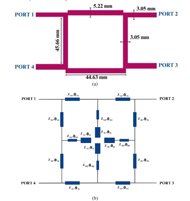
Figure 1: Layout of (a) conventional BLC and (b) proposed SBBLC with ETSTL.
In recent times, DB components have earned a great deal of attention as a result of the potential opportunities they provide for use in BM [11] and crossovers [12]. In response to this, a number of other DBBLCs have been created. A DBBLC is often created by simply exchanging every quarter-wave line from a single-band branch-line coupler (SBBLC) with an equal number of DB quarter-wave blocks. This is the most common method. In order to investigate DB approaches, many strategies are used. These techniques include -shaped lines [13], T-network [14], open-ended stub [15], coupled line [16], feature-based optimization [17], port extension [18, 19], and cross coupled [20].
Two novel couplers, a Single-Band Branch-Line Coupler (SBBLC) and a Dual-Band Branch-Line Coupler (DBBLC), are proposed using Elongated T-Shape Transmission Lines (ETSTL). The same SBBLC structure can be adapted for DBBLC operation by adjusting the electrical length of the transmission line and the open stub. Through even-odd mode analysis, the impedance values are determined. It was necessary to model, build, and evaluate a coupler operating at 0.9 GHz and 2.4 GHz using a FR4 substrate in order to verify the idea. The remaining sections of the article may be organized as follows: section II provides an illustration of the work that is suggested, section III presents the findings and discussion, and section IV draws the conclusion.
II. PROPOSED WORK
The conventional BLC is shown in Fig. 1 (a). It is composed of four branches with quarter-wavelength, which are two series arms with an impedance of 35.35 and two shunt arms with an impedance of 50. Using a FR4 substrate with a thickness of 1.6 mm and value of 4.4, the conventional coupler dimensions are 51.256.6 mm. However, the size of the device is a disadvantage of this typical technique, which is one of its problems.
A. Design of proposed SBBLC
Figure 1 (b) illustrates the construction of a SBBLC that makes use of an ETSTL with series and shunt arm. This kind of coupler is responsible for providing a connectivity between the transmission lines that have open stubs.
An Elongated T-Shape as seen in Fig. 2 comprised of three transmission lines and a stub.
The three impedances that are associated with ETSTL are Z, Z, and Z. The electrical lengths that correlate to these impedances are , , and . The impedance of the transmission lines is represented by the symbols Z and Z in Fig. 2. The impedance of the stub is represented by Z. The symbols and may be used to represent the electrical lengths of the transmission lines. The electrical length of the stub is represented by the symbol .
B. Design of proposed DBBLC
The coupler is designed to operate at two different frequency bands, hence termed DBBLC. The operating frequencies are f 0.9 GHz and f 2.4 GHz, where the frequency ratio, p 2.66, .
| (1) | |
| (2) | |
| (3) |
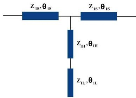
Figure 2: Elongated T-Shape Transmission Line.
Frequency ratio is determined by equation (1). To further comprehend the phase connection between these frequencies, we compute two crucial angles. The first angle simplifies to about .
The second angle is roughly , calculated using equation (3). These angles, determined from the frequency ratio, reflect the phase angles connected with the frequencies, allowing for a clear understanding of their phase connection. In the proposed structure, is divided into for transmission line and stub, respectively.
C. Analysis of the proposed coupler
An even and odd mode equivalent circuit analysis is performed on the ETSTL, as can be seen in Fig. 3. When it comes to identifying the impedance and electrical lengths that are required, in order to obtain the acceptable coupling qualities, the findings of this research are useful in understanding what those dimensions are [10].
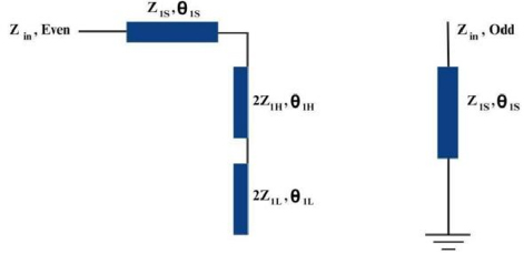
Figure 3: Even and odd mode analysis of ETSTL.
The even and odd mode impedance of the proposed ETSTL can be written as
| (4) | ||
| (5) |
where
| (4a) |
| (4b) |
It is possible to express the typical transmission line for even and odd mode impedance as
| (5) | ||
| (6) |
The impedance characteristics may be computed in the following manner, taking into account both the conventional design and the design that was suggested:
| (7) | ||
| (8) |
where
| (8a) |
| (8b) |
| (8c) |
Figure 4 is a representation of the equivalent series arm transmission line. The impedances that are distinctive of the series arms are what give them their identity Z, Z, and Z. As a result of these arms being linked in series between the ports, it is possible to send signals or power from one port to another. In addition to being in charge of the coupling mechanism, the series arms are also responsible for determining how power is distributed among the ports.
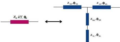
Figure 4: Equivalent series arm transmission line.
The equivalent shunt arm transmission line is shown in Fig. 5. The shunt arms are represented by the impedances Z, Z, Z. The ground reference and the series arms are linked to these arms in a parallel fashion and provide the connection. It is the shunt arms that are responsible for ensuring that the ports remain isolated and that the impedance matching that is sought is maintained. In addition to this, they further contribute to the overall coupling qualities of the coupler.
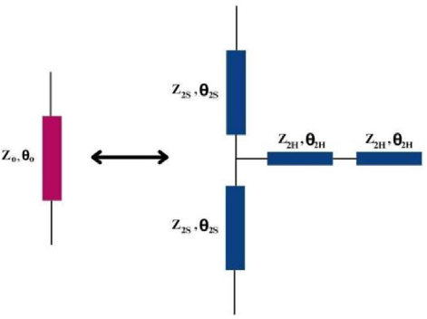
Figure 5: Equivalent shunt arm transmission line.
The design curve for ZZis shown in Fig. 6, against the value of for the series arm. To get the value of it is necessary to solve equations (7) and (8) mathematically. This allows one to derive the impedance of ZZby altering the electrical length. Under the assumption that K is equal to one, is equal to for 20. In order to produce an SBBLC using ETSTL on a FR4 substrate with a dielectric constant and a substrate thickness of 1.6 mm, it is necessary to replace the traditional BLC with similar ETSTL units.
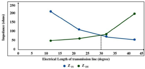
Figure 6: Impedance versus electrical length of series SBBLC.
Figure 6 shows the design curve for Z Z versus for a series arm by solving equations (7) and (8) graphically to obtain the impedance of ZZby varying the electrical length by assuming K 1, in order to determine the value.
Figure 7 shows the design curve for ZZ versus for the shunt arm by solving equations (7) and (8) graphically to obtain the impedance of ZZby varying the electrical length by assuming K=1,=, in order to determine . The following values are obtained for the ETSTL for SBBLC (Series Arm), Z=61.26, Z=69.76, Z=61.26 when we substitute the electrical length values as in equations (7) and (8). In same way, for shunt arm, the impedance values are Z=86.60, Z98.72, Z=86.60. Table 1 shows the series and shunt value analysis of SBBLC.
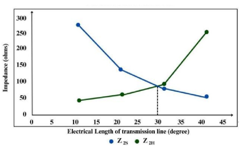
Figure 7: Impedance versus electrical length of shunt SBBLC.
Table 1: Series and shunt value analysis of SBBLC
| ARM | IMPEDANCE () | WIDTH(mm) | LENGTH(mm) |
| SERIES | Z61.26 Z69.76 Z61.26 |
2.14 | 15.43 |
| 1.66 | 10.38 | ||
| 2.14 | 10.28 | ||
| SHUNT | Z86.60 Z98.72 Z86.60 |
1.03 | 15.81 |
| 0.73 | 10.64 | ||
| 1.03 | 10.54 |
Figure 8 (a) shows the impact of Impedance versus electrical length for series arm of DBBLC. In the equivalent series arm, the characteristics impedance of the coupler for k 1, Zat Z tends to fall between 327 to 229. Similarly for k 2, Zat Z tends to fall between 166 to 110 which is not feasible for fabrication because the impedance is not suitable for the FR4 substrate. When k 3, Zat Z tends to fall between 102 to 68 which provides the feasibility to fabricate the FR4 substrate of the proposed design.
Figure 8 (b) shows the impact of Impedance versus electrical length for shunt arm of DBBLC. In the equivalent shunt arm, the power division ratio of the equal power division coupler for k=1, Z at Z /2 tends to fall between 475 to 332. Similarly for k=2, Z at Z/2 tends to fall between 240 to 160 which is not feasible for fabrication because the impedance is not suitable for a FR4 substrate. Hence, when k=3, Z at Z/2 tends to fall between 155 to 99 provides the feasibility to fabricate in the FR4 substrate of the proposed design. The overall parameter value obtained on series and shunt arm for DBBLC are illustrated in Table 2.
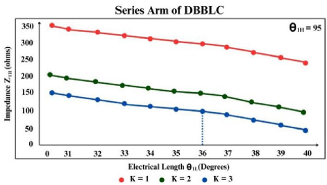
Figure 8: (a) Impedance versus electrical length for series arm of DBBLC.
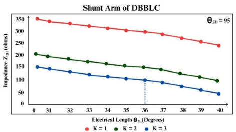
Figure 8: (b) Impedance versus electrical length for shunt arm of DBBLC.
Table 2: Calculated parameter values of DBBLC
| Circuit Parameters () | Structure Parameters (mm) | |
| Series | Z30.729 Z83.91 Z30.729 |
l30.86 mm l49.97 mm l17.69 mm w6.35 mm w1.11 mm w6.35 mm |
| Shunt | Z43.46 Z118.60 Z43.46 |
l49.24 mm l51.21 mm l18.09 mm w3.83 mm w0.42 mm w3.83 mm |
III. PERFORMANCE ANALYSIS
Evaluation of the designed architecture is done in this section. Commercial electromagnetic simulation software ADS is used for the optimization of physical parameters. For the conventional BLC, characteristic impedance of the shunt arm is 50, and impedance of the series arm is 35.35.
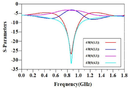
Figure 9: Simulation result of conventional BLC.
Figure 9 shows the S-parameters of the conventional BLC. From the plot, the output characteristics of the BLC can be observed, including the insertion loss, coupling, isolation, and return loss at the output ports.
A. Simulation result of proposed SBBLC
Figures 10 (a) and (b) show the simulation results of SBBLC. Ideally, S and S should be greater than -15 dB and the proposed SBBLC has achieved -24.8 dB and -22.4 dB, respectively.
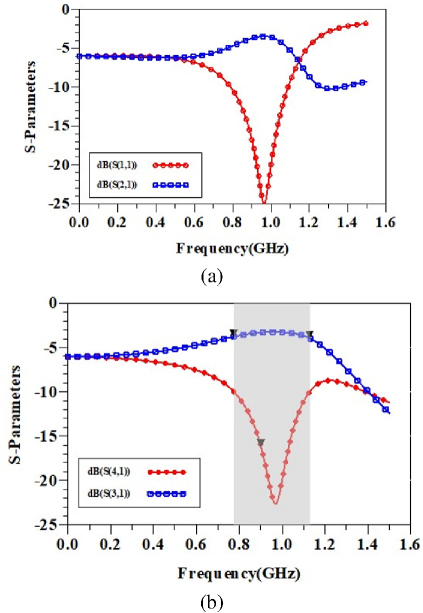
Figure 10: (a) Simulation result of Return Loss S and Insertion Loss S of SBBLC and (b) simulation result of Isolation S and Coupling S of SBBLC.
Ideally, S and S should be -3 dB and the proposed SBBLC achieves -3.5 dB and -3.2 dB, respectively. When compared to a conventional coupler, SBBLC achieved 55% size reduction and 33% FBW.
B. Simulation result of proposed DBBLC
For the DBBLC, the center frequency is located at 0.9 to 2.4 GHZ, maximal measured insertion losses |S21|/|S31| are -3.5 to -4.7 dB and -3.6 to -3.7 dB, respectively.
S and S should be greater than -15 dB and the proposed DBBLC has achieved -16.7 to -18.4 dB and -17.6 to -18.1 dB for 0.9 GHz and 2.4 GHz, respectively. Similarly, S and S should be -3 dB and the proposed DBBLC has achieved -3.5 to -4.7 dB and -3.6 to -3.7 dB for 0.9 GHz and 2.4 GHz, respectively.
FBW achieved nearly 400 MHz (44%). The size of the proposed coupler is reduced by 67% compared to the conventional structure.
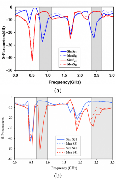
Figure 11: (a) S and S parameter value analysis of DBBLC and (b) S and S parameter value analysis of DBBLC.
Suggested BLC simulated S-parameters are shown in Figs. 11 (a) and (b). The down peaks show the midpoint frequencies of the two comparison pass bands. The most that may be seen in the amplitude imbalance between the output ports is 0.3 dB. At mid-frequency ranges, isolation loss, and return loss are both significantly below -20 dB.
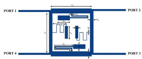
Figure 12: Layout of the DBBLC.
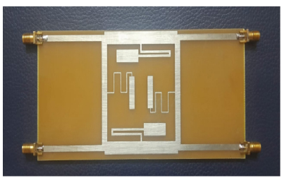
Figure 13: Fabricated prototype of the DBBLC.
Figure 12 shows the layout of the DBBLC. Following fabrication (Fig. 13) and measurement of the coupler prototype, the suggested design idea is evaluated to see whether it is feasible. Both the SNA4400 network analyzer and ADS Keysight were used to do simulations and analyses on the proposed DBBLC.
From the above discussions, the proposed model has dimensions of 0.29g 0.32g (g is the full transmission wavelength at the center frequency).
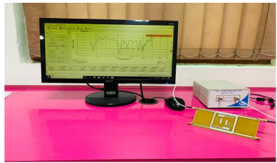
Figure 14: Experimental setup for DBBLC.
Table 3: Proposed architectures performance comparison
| F (GHz) | Return Loss (dB) | Isolation (dB) | Size (g) | FBW(%) | |
| SBBLC | 0.9 | 24.83 | 24.47 | 0.17 0.18 |
33 |
| DBBLC | 0.9/2.4 | 16.7/ 18.41 | 17.8/18.1 | 0.28 0.32 |
44 |
Table 4: Comparison between proposed SBBLC and others
| Ref. | F (GHz) | Return Loss (dB) | Isolation (dB) | Size (g) | Size Reduction(%) | FBW(%) |
| [2] | 2.45 | 20 | 28 | - | 29 | 50 |
| [3] | 3.55 | 30.69 | 29.28 | 0.27 0.16 |
- | 32.2 |
| [4] | 2.45 | 21.7 | 36.2 | - | 64.21 | 22.08 |
| [6] | 2.82 | 29.5 | 31.3 | 0.29 0.26 |
- | - |
| [7] | 3.5 | 8 | 11 | - | 31 | 34.4 |
| This SBBLC | 0.9 | 24.83 | 24.47 | 0.170.18 | 55 | 33 |
Table 5: Comparison between proposed DBBLC and other works
| Ref. | F (GHz) | Return Loss (dB) | Insertion Loss (dB) | Coupling(dB) | Isolation (dB) | Phase Difference (deg) | Size (g) | FBW(MHz) |
| [16] | 0.756/1.42 | 15 | 3.35/3.74 | 4.0/4.10 | 14 | 87,89 | - | - |
| [13] | 0.9/2.0 | 26.8/35.6 | 3.5/3.4 | 3.1/3.3 | 23.4/27.2 | - | 0.79x0.1 | - |
| [15] | 0.9/1.63 | 20 | 3.2/3.5 | 3.3/4.1 | 14 | 90.3,89.2 | 0.53x0.34 | - |
| [14] | 0.92/2.03 | Below 24/19 | 3.17/3.76 | 3.50/3.83 | Below 24/19 | 89.1,89.6 | - | - |
| [17] | 0.92/1.9 | 36.4/23.5 | 3.18/3.37 | 3.14/3.46 | 33.8/39.8 | 90,90 | 0.18x0.15 | - |
| [19] | 1.0/2.0 | 36.7/25.3 | 3.3/3.1 | 3.1/3.7 | 32.9/29.9 | 90,89 | - | - |
| [20] | 0.99/1.97 | 35.5/24.1 | 3.22/2.95 | 3.06/3.53 | 32.6/22 | 91,90 | - | - |
| This Work (DBBLC) | 0.9/2.4 | 16.7/18.41 | 3.5/4.7 | 3.6/3.7 | 17.8/18.1 | 86,91 | 0.28x0.32 | 400 |
The even-odd mode analysis and practical design impedance curves provide explicit design formulae. A 0.9/2.4 GHz DBBLC is manufactured for the purpose of verification. The findings from the simulations and the measurements are in good agreement. The coupler has an easy-to-understand architecture with strategically placed ports, and it also provides some leeway in the design for potential other uses. Figure 14 shows the experimental setup for DBBLC.
Compared with other works (see Tables 4 and 5), the suggested architecture output performs better than other existing architectures. DBBLC exhibits significant performance slightly higher than SBBLC.
IV. CONCLUSION
In this work, two novel couplers for SBBLC and DBBLC are proposed. In addition, design equations are offered through the use of even-odd mode analysis. The results of the simulations indicate that the coupler constructed has good degrees of matching and isolation at both center frequencies. Folding the stub towards the inner section of the coupler in order to make it suitable for manufacture is one of the methods used to reduce the size of the coupler. By using a simple design formula, the coupler presented has the potential to provide the needed output at the dual frequencies stated. The architecture proposed has a number of benefits, including a small size and FBW. Both the simulated and measured results of the structures exhibit a high degree of consistency.
REFERENCES
[1] K. V. Phani Kumar and S. S. Karthikeyan, “Miniaturized quadrature hybrid coupler using modified T-shaped transmission line for wide-range harmonic suppression,” IET Microwaves, Antennas, and Propagation, vol. 10, no. 14, pp. 1522-1527, Nov. 2016.
[2] W. Nie, K.-D. Xu, M. Zhou, L.-B. Xie, and X.-L. Yang, “Compact narrow/wide band branch-line couplers with improved upper-stopband,” International Journal of Electronics and Communications, vol. 98, pp. 45-50, Jan. 2019.
[3] A. A. Abdulbari, S. K. A. Rahim, M. Z. A. Abd Aziz, K. G. Tan, N. K. Noordin, and M. Z. M. Nor, “New design of wideband microstrip branch line coupler using T-shape and open stub for 5G application,” International Journal of Electrical and Computer Engineering, vol. 11, no. 2, pp. 1346-1355, Apr. 2021.
[4] M. Y. O. Elhiwaris, S. K. A. Rahim, and U. A. K. Okonkwond, N. M. Jizat, “Miniaturized size branch line coupler using open stubs with high-low impedances,” Progress in Electromagnetics Research Letters, vol. 23, pp. 65-74, Apr. 2011.
[5] K.-S. Choi, K.-C. Yoon, J.-Y. Lee, C.-K. Lee, S.-C. Kim, K.-B. Kim, and J.-C. Lee, “Compact branch-line coupler with harmonics suppression using meander T-shaped line,” Microwave and Optical Technology Letters, vol. 56, no. 6, pp. 1382-1384, June 2014.
[6] A. Rezaei and L. Noori, “Microstrip hybrid coupler with a wide stop-band using symmetric structure for wireless applications,” Journal of Microwaves, Optoelectronics and Electromagnetic Applications, vol. 17, no. 1, Mar. 2018.
[7] N. A. M. Shukor and N. Seman, “Enhanced design of two-section microstrip-slot branch line coupler with the overlapped /4 open circuited lines at ports,” Wireless Personal Communications, vol. 88, pp. 467-478, Nov. 2015.
[8] K. V. Phani Kumar and S. S. Karthikeyan, “Microstrip low pass filter with flexible roll-off rates,” International Journal of Electronics and Communications, vol. 86, pp. 63-68, Jan.2018.
[9] S. Roshani, S. I. Yahya, S. Roshani, and M. Rostami, “Design and fabrication of a compact branch-line coupler using resonators with wide harmonics suppression band,” Electronics, vol. 11, no. 793, Mar. 2022.
[10] F. Hosseinkhani and S. Roshani, “A compact branch-line coupler design using low-pass resonators and meandered lines open stubs,” Turkish Journal of Electrical Engineering & Computer Sciences, vol. 26, pp. 1164-1170, 2018.
[11] A. M. Zaidi, M. T. Beg, B. K. Kanaujia, J. Kishor, and K. Rambabu, “A novel dual band branch line coupler and its application to design a dual band 4 X 4 Butler matrix,” IEEE Access, vol. 8, Apr.2020.
[12] M. A. Maktoomi, M. S. Hashmi, and F. M. Ghannouchi, “Systematic design technique for dual-band branch-line coupler using T- and Pi-networks and their application in novel wideband-ratio crossover,” IEEE Transactions on Components, Packaging and Manufacturing Technology, vol. 6, no. 5, May 2016.
[13] X.-Y. Zhang and J.-C. Lee, “A dual-band branch-line coupler with ultra-wideband harmonic suppression,” Journal of Electromagnetic Engineering and Science, vol. 23, no. 1, pp. 57-62, Jan.2023.
[14] H. Zhang and K. J. Chen, “A stub tapped branch-line coupler for dual-band operations,” IEEE Microwave and Wireless Components Letters, vol. 17, no. 2, Feb. 2007.
[15] W. Feng, X. Duan, Y. Shi, X. Y. Zhou, and W. Che, “Dual-band branch-line couplers with short/open-ended stubs,” IEEE Transactions on Circuits and Systems—II: Express Briefs, vol. 67, no. 11, Nov. 2020.
[16] W. Feng, Y. Zhao, W. Che, H. Chen, and W. Yang, “Dual-/tri-band branch line couplers with high power division isolation using coupled lines,” IEEE Transactions on Circuits and Systems—II: Express Briefs, vol. 65, no. 4, Apr. 2018.
[17] S. Koziel and A. Lukasiewicz, “Fast simulation-driven feature-based design optimization of compact dual-band microstrip branch-line coupler,” International Journal of RF and Microwave Computer-Aided Engineering, vol. 26, no. 1, Jan. 2016.
[18] M. A. Maktoomi, M. S. Hashmi, and F. M. Ghannouchi, “A dual-band port-extended branch-line coupler and mitigation of the band-ratio and power division limitations,” IEEE Transactions on Components, Packaging and Manufacturing Technology, vol. 7, no. 8, pp. 1313-323, Aug.2017.
[19] H. Kim, B. Lee, and M. J. Park, “Dual-band branch-line coupler with port extensions,” IEEE Transactions on Microwave Theory and Techniques, vol. 58, no. 3, pp. 651-655, 2010.
[20] M. J. Park and B. Lee, “Dual-band, cross coupled branch line coupler,” IEEE Microwave and Wireless Components Letters, vol. 15, no. 10, pp. 655-657, 2005.
BIOGRAPHIES

G. Srividhya is currently pursuing her Ph.D. in Information and Communication Engineering at Anna University, Chennai, India. She earned her M.Tech. in VLSI Design from Bharath University, Chennai, India (2013), and B.E. in Electronics and Communication Engineering from SCSVMV University, Kanchipuram, India (2011). She serves as Assistant Professor in the Department of Electronics and Communication Engineering at Panimalar Engineering College, Poonamallee, Chennai, India. She has published extensively in international journals and conferences. Her research interests include VLSI design, RF devices, antenna systems, artificial intelligence, and machine learning, bridging traditional electronics with emerging technologies in modern communication systems.

S. Maheswari received the Ph.D. degree in Microwave Engineering and the M.E. degree in Applied Electronics from Sathyabama Institute of Science and Technology, Chennai, India, in 2016 and 2009, respectively. She received the B.E. degree in ECE from University of Madras. Her area of research includes microwave and millimeter wave circuits. She has more than two decades of teaching experience. Currently she is working as a Professor in Panimalar Engineering College, Chennai, India. She is a recognized supervisor for doing research in Anna University. She has published more than 30 papers in Web of Science, Scopus indexed journals, and IEEE conferences. She is a Fellow of IETE.
ACES JOURNAL, Vol. 40, No. 6, 541–549
doi: 10.13052/2024.ACES.J.400607
© 2025 River Publishers