Beam-reconfigurable Antenna Based on Planar Inductor with Mn-Zn Ferrite
Meng Yin, Cheng Ju, Wei-Hua Zong, and Shandong Li
College of Electronic Information
Qingdao University, Qingdao 266071, China
2018206231@qdu.edu.cn, jucheng719@qdu.edu.cn, zongweihua@qdu.edu.cn, lishd@qdu.edu.cn
Submitted On: October 30, 2024; Accepted On: March 31, 2025
ABSTRACT
This paper presents a beam-reconfigurable antenna design adopting distributed inductors, Mn-Zn ferrite, and static magnetic fields. The proposed antenna consists of one driven patch, two parasitic patches, and a full ground plane. Each parasitic patch is loaded with a distributed inductor with positive inductance. The patch antenna has a symmetric configuration and a broadside pattern. A Mn-Zn ferrite slab is added to one inductor to reduce its self-resonant frequency and change its inductance from positive to negative which results in unsymmetric field distributions and a tilted radiation beam. A static magnetic field is applied to the ferrite material further to adjust the tilted angle of the radiation beam. The proposed antenna works at five modes with reconfigurable beams of 0 (0), 15 (90, 270) and 28 (90, 270).
Index Terms: Magnet, Mn-Zn ferrite, negative inductances, reconfigurable beams.
I. INTRODUCTION
Beam-reconfigurable antennas provide interference-free, power-saving, and highly secured end-to-end communication making them attractive in 5G and satellite communication systems [1–4]. Extensive research has been conducted on beam reconfigurable antenna design [3–13], in the design of which PIN diodes [3–9], varactors [10, 11], and phase shifters [12, 13] are adopted to control feeding networks, connections among metallic portions, or phase shifting between antenna elements. Table 1 compares the published beam reconfigurable antennas. A common characteristic of these designs is the need to introduce a DC power supply for control. This requires the design of DC bias circuits, which involves a large number of lumped components, increases design complexity, occupies space on the circuit board, and potentially introducing losses that lead to gain reduction during the soldering of these lumped components.
To address these issues, this article presents a novel technique of beam reconfiguration using tunable inductors. The inductors are loaded with magnetic material and controlled by a magnetic field to tune both the inductance and the antenna beam. Compared to traditional beam reconfigurable antennas, the proposed design does not require a DC bias circuit, and the fabrication only involves grounding the inductor, simplifying the manufacturing process, and reducing design complexity. Magnetic materials and magnetic fields have been adopted in inductors to improve [14–19] and tune [20–23] inductance. To the best of the authors’ knowledge, this article presents the first design of a beam-reconfigurable antenna by using magnetic field control.
Table 1: Comparison of the published beam reconfigurable antennas
| Ref. | Freq.(GHz) | Tunable andLumped Components | Beam States | Gain(dB) |
| [3] | 3.5 | 4 PIN, 4 L, 4 R, 4 P | 8 | 4.9 |
| [4] | 3.8 | 8 PIN, 16 L, 32 C, 8 R, 8 P | 3 | 3.8 |
| [5] | 3.6 | 8 PIN, 8 L, 8 C, 8 R, 8 P | 5 | 11.85 |
| [6] | 3.7 | 12 PIN, 4 L, 12 P | 12 | 4.61 |
| [7] | 5.3 | 8 PIN, 9 L, 12 C, 1 R, 8 P | 4 | 7.04 |
| [10] | 3 | 2 Var, 2 C, 2 P | 5 | N.A. |
| [11] | 5.8 | 3 Var, 3 L, 3 C, 3 R, 3 P | 3 | 6.5 |
| [12] | 11.75 | Phase shifter | 6 | 20 |
| [13] | 4.8 | 28 PIN, 12 C, 28 P | 9 | 7.8 |
| This Work | 2.4 | 0 | 5 | 6.02 |
PIN is PIN diode, L is inductor, C is capacitor, R is resistor, P is power, Var is varactor, unit is dBic
The proposed antenna is a patch antenna with two parasitic patches. Two tunable inductors are loaded in the two parasitic patches. A Mn-Zn ferrite slab and magnet are adopted to tune each inductor’s inductance. The proposed antenna beam works at five states with main beam points to 28 (270), 15 (270), 0 (0), 15 (90), and 28 (90), respectively.
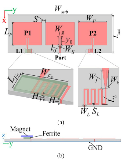
Figure 1: Configuration of the proposed antenna: (a) top view (without magnet) and (b) side view (with magnet).
Table 2: Dimensions of the proposed antenna
| Parameter | W | L | W | L | W | W | y | l | s |
| Value (mm) | 150 | 53 | 41.5 | 32.8 | 1.8 | 3.7 | 10.6 | 11 | 5.5 |
| Parameter | H | W | L | H | W | L | S | W | W |
| Value (mm) | 0.8 | 5 | 9 | 0.5 | 0.4 | 3 | 0.5 | 5.5 | 1.9 |
Table 3: Radiation patterns of the proposed antenna
| Mode | Left Inductor | Right Inductor | Measurement | Simulation | ||
| Main Beam (,) | Gain (dB) | Main Beam (,) | Gain (dB) | |||
| 1 | - | - | (0, 0) | 6.82 | (0, 0) | 6.84 |
| 2 | - | With ferrite | (15, 90) | 6.22 | (15, 90) | 6.58 |
| 3 | With ferrite | - | (15, 270) | 6.22 | (15, 270) | 6.58 |
| 4 | - | With ferrite and magnet | (28, 90) | 6.07 | - | - |
| 5 | With ferrite and magnet | - | (28, 270) | 6.07 | - | - |
II. ANTENNA DESIGN
Figure 1 shows the configuration of the proposed antenna. The antenna consists of three rectangular patches and a full ground (GND) printed on a 0.8 mm thick Rogers RO4003 substrate with 3.55 and tan0.0027. The three patches are identical in size and shape. The center patch is directly fed through a microstrip line, while the other two patches (P1 and P2) are fed by coupling, with each loaded with a meander-shaped inductor shorted to the ground plane. The antenna configuration derives from the one in [10] by replacing the varactors with tunable inductors. The patch antenna is symmetric along the y-axis, resulting in a broadside radiation pattern. A piece of Mn-Zn ferrite slab, with a thickness of 0.5 mm, is mounted on top of one inductor to realize negative inductance, while the other inductor, which has no ferrite slab, exhibits positive inductance. The discrepancy in inductance values between the two inductors results in a tilted beam. Furthermore, applying a magnetic field with a magnet results in a larger scanning beam. The proposed antenna operates at a resonant frequency of 2.4 GHz. The antenna dimensions are listed in Table 2.
Table 3 shows the radiation patterns of the proposed antenna. At Mode 1, both inductors are without a ferrite slab or magnet, resulting in equal inductance values and broadside patterns. At Mode 2, the inductance on the right side is loaded with a ferrite slab, resulting in a beam tilted 15 and 90. At Mode 3, the antenna beam tilts to the opposite direction of Mode 2 (15 and 270) with the ferrite slab loaded on the left inductor. At Mode 4/5, the ferrite slab on the right/left inductor is subjected to a magnetic field from a magnet, and a larger tilted beam is obtained at 28 and 90, 270.
A. Reconfigurable beam design with lumped inductor
Two lumped inductors are used to replace the two meandered line inductors (L1 connected to P1 and L2 connected to P2) to evaluate the inductance values required to obtain beam reconfiguration. Antenna performance was simulated using the Ansys high-frequency structure simulator (HFSS) software.
Table 4: States of proposed antenna with lumped inductors
| State | L1 (nH) | L2 (nH) | Beam direction (,) |
| 1 | 10 | 10 | (0, 0) |
| 2 | 1 | 10000 | (1, 270) |
| 3 | 0 | 100 | (4, 270) |
| 4 | 100 | 0 | (4, 90) |
| 5 | -10 | 0 | (10, 270) |
| 6 | 0 | -10 | (10, 90) |
| 7 | -20 | 260 | (13, 270) |
| 8 | 260 | -20 | (13, 90) |
| 9 | -3 | 260 | (32, 270) |
| 10 | 260 | -3 | (32, 90) |
| 11 | 160 | -3 | (30, 90) |
| 12 | 360 | -3 | (32, 90) |
| 13 | 460 | -3 | (33, 90) |
| 14 | 260 | -1 | (33, 90) |
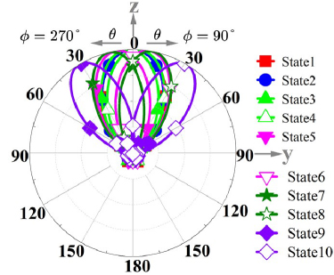
Figure 2: Normalized radiation patterns for different states of yoz.
Table 4 presents 14 states with different beams and Fig. 2 illustrates the corresponding radiation patterns. As shown in Table 4 and Fig. 2, at State 1, L1L210 nH, the antenna beam points to the z direction (0 and 0). At State 2, L1 and L2 are both positive with a great difference in value (9999 nH), and a small tilted angle of 1 is obtained in the elevation plane. This indicates that loading inductors with different values in the two parasitic patches introduces a beam tilted to the side of the smaller inductor. However, a minimal tilted angle is obtained when both inductors are positive. In the cases of States 3-6, one of the two patches is directly shorted to the ground plane without loading an inductor, while the other patch is loaded with an inductor. A negative inductor (-10 nH) achieves a larger tilted angle compared to a positive inductor (100 nH), indicating that negative inductors are more effective in achieving larger tilted beams than positive ones. The comparison of States 7-10 indicates that when the inductance values of the two inductors have opposite signs, a smaller absolute value of the negative inductance leads to a larger tilted angle in the radiation pattern. In States 9-10, a significant tilted angle was achieved, 32, where one inductor is a positive inductance of 260 nH and the other is a negative inductance of -3 nH. Comparing State 10 with States 11-14, it can be seen that the titled beam angle increases with the increase of the positive inductor’s inductance value or the negative inductor’s inductance absolute value. It seems that the beam angle reaches a stable value at State 9-10, since the beam angle only increases by 1 when the positive inductor increases from 260 to 460 nH or the negative inductor decreases from -3 to -1 nH. In section IIB, a distributed inductor with an inductance around 260 nH will be designed using meandered lines, and the inductance is tuned to a negative value around -3 nH by loading a ferrite slab.
B. Design of distributed inductors
Based on the discussion above, different tilted beams are obtained by loading different inductors in P1 and P2. Meandered lines are utilized to design a positive inductor, avoiding the need for via holes or metallic bridges that would be required for a spiral-shaped inductor [17]. In the proposed inductor, shown in Fig. 1, one terminal is directly connected to the parasitic patch, while the other terminal, located at the edge of the board, connects to the ground plane via a soldered copper wire. Figure 3 shows the inductor’s characteristics varying with dimensions. As shown, the inductor reaches its maximum positive value at its self-resonant frequency and decreases to a negative value dramatically with the increase in frequency. Furthermore, the inductor’s resonant frequency decreases with the increase of the line’s length of L, width of W, and spacing of S. The inductor resonates at the working frequency of 2.4 GHz when L3 mm, W0.4 mm, S0.5 mm, with its peak inductance of 260 nH which meets the requirement of positive inductor’s inductance value at States 9-10 in Table 4. A negative inductor with an inductance around -3 nH is required based on the meandered line-shaped configuration working at States 9-10.
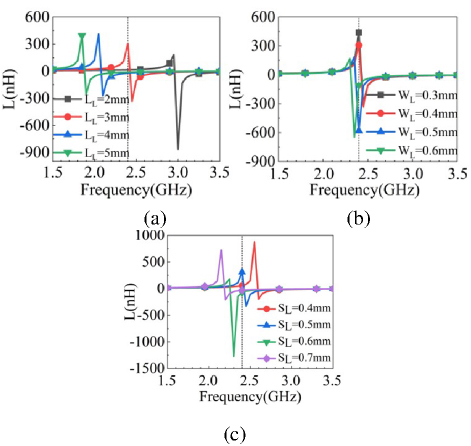
Figure 3: Impact of parameter dimensions on inductance: (a) L, (b) W, and (c) S.
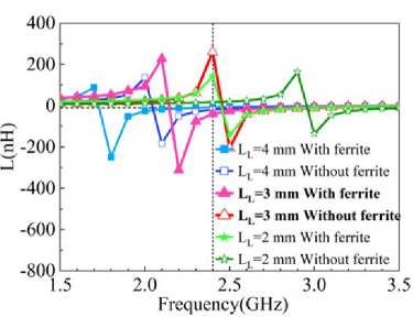
Figure 4: Changes of inductance by adding ferrite slab.
Based on the inductors designed above, this paper presents an approach of using magnetic material to change the inductance from positive to negative by reducing the inductor’s self-resonant frequency [17, 24]. Mn-Zn ferrite is chosen to be loaded onto one inductor as shown in Fig. 1 (a), due to its high magnetic permeability and sensitive response to magnetic fields. Figure 4 shows the inductor’s inductance with/without the ferrite slab with W0.4 mm and S0.5 mm. When L3 mm, with a loaded ferrite slab, the self-resonant frequency of inductors decreases from 2.4 GHz to 2.1 GHz, while its inductance changes from 260 nH to -20 nH. When L2 mm, both resonate frequencies are higher than 2.4 GHz, resulting in two positive inductances of the cases without/with ferrite slab. When L4 mm, both resonate frequencies are lower than 2.4 GHz, resulting in two negative inductances of the cases without/with ferrite slab. In conclusion, an inductor resonating at its working frequency (2.4 GHz) is an ideal choice to obtain negative inductance by adding a ferrite slab.
Figure 5 gives a simulated magnetic field distribution on the inductor with/without ferrite slab. As shown, the magnetic fields increase significantly with the loaded ferrite slab, which leads to a decrease in self-resonant frequency and an increase in inductance at frequencies below resonant frequencies, which agrees with the trend shown in Fig. 5.
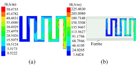
Figure 5: Simulation of H-field distribution of the proposed inductor: (a) without ferrite and (b) with ferrite.
C. Reconfigurable beam design with distributed inductors
By adopting the two distributed inductors with meandered line shapes and loading with a ferrite slab (as shown in Fig. 1), beam reconfiguration is obtained with three modes given in Table 2. At Mode 1, both inductors are unloaded with a ferrite slab, resulting in the same inductance and broadside pattern. At Mode 2, the right inductor has negative inductance by loading with a ferrite slab, and the left one has positive inductance without ferrite loading, resulting in the main beam being tilted 15 to the negative inductor. At Mode 3, the antenna beam is tilted to the left side when a ferrite slab is loaded on the left inductor.
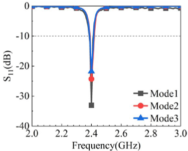
Figure 6: S plots of the proposed antenna.
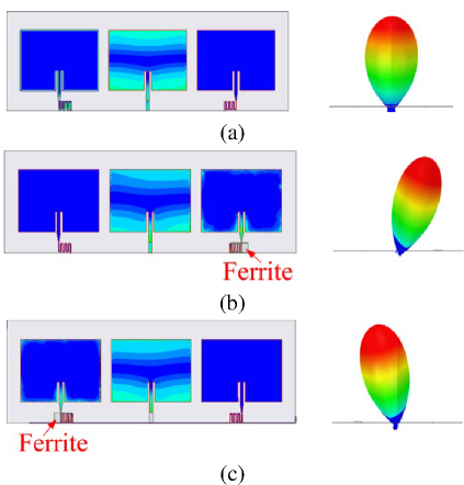
Figure 7: E-field distribution and radiation pattern: (a) Mode 1, (b) Mode 2, and (c) Mode 3.
S plots of the proposed antenna in the three modes are given in Fig. 6. The antenna resonates at 2.4 GHz with an overlapping bandwidth of 2.39-2.42 GHz in the three modes. Figure 7 presents the proposed antenna’s simulated electric field distributions and radiation patterns at different modes. At Mode 1, the electric field distributions and radiation patterns show symmetry about the antenna’s middle axial due to its symmetric configuration. At Mode 2/3, the electric field is more concentrated around the patch loaded with a ferrite slab, resulting in the antenna beam being tilted to the same side.
Table 5 illustrates the impact of varying the ferrite slab’s dimensions on the antenna’s radiation pattern. Specifically, as the thickness (H) of the ferrite slab increases, the tilted beam angle increases while the gain decreases. To achieve an optimal balance between the beam angle and gain, an H of 0.5 mm was selected. Additionally, the maximum beam angle and gain were observed when W5 mm and L9 mm.
Table 5: Ferrite slab’s size influence on antenna pattern
| Parameter | Value (mm) | Beam (,) | Gain (dB) |
| H | 0.45 | (13, 90) | 5.0 |
| 0.5 | (18, 90) | 4.9 | |
| 0.55 | (20, 90) | 4.6 | |
| W | 4.5 | (13, 90) | 4.8 |
| 5 | (18, 90) | 4.9 | |
| 5.5 | (15, 90) | 4.6 | |
| L | 8.5 | (15, 90) | 4.7 |
| 9 | (18, 90) | 4.9 | |
| 9.5 | (16, 90) | 4.6 |
Based on the discussion of section IIA, an increase in the value of negative inductance will lead to a larger tilted beam angle. A permanent magnet was adopted to enforce static magnetic fields on the Mn-Zn ferrite. Magnetic fields distributions in the ferrite slab with/without the magnet have been simulated by using ANSYS Maxwell and are given in Fig. 8. As shown, by applying static magnetic fields, the magnetic induction intensity increases more than two times. The effect of the magnet on the inductor’s inductance and the tilted beam cannot be simulated by ANSYS Maxwell or HFSS directly due to the limitations of each software. Maxwell can only model the impact of static magnetic fields on the magnetic properties but cannot account for the dynamic behavior of the inductor or antenna at higher frequencies. HFSS can accurately model the inductor’s inductance and antenna patterns. However, it does not support the simulation of static magnetic field’s effect on the inductor. The enhancement of tilted beam angle through the use of a magnet will be validated through measurement in section III.
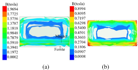
Figure 8: Simulated B-field distribution of the magnet: (a) with ferrite and magnet and (b) with magnet.
III. FABRICATION AND MEASUREMENT
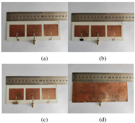
Figure 9: Photographs of proposed antenna: (a) top layer of Mode 1, (b) top layer of Mode 3, (c) top layer of Mode 5, and (d) bottom layer.
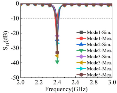
Figure 10: Measured and simulated Sof the proposed antenna.
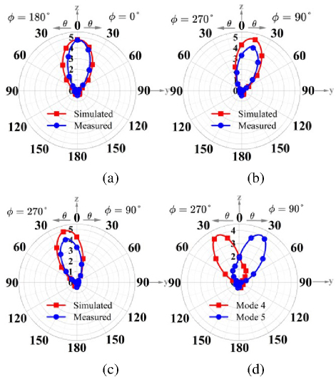
Figure 11: Measured and simulated radiation patterns for different modes of yoz: (a) Mode 1, (b) Mode 2, (c) Mode 3, and (d) Modes 4 and 5.
The proposed antenna was fabricated and measured to validate the simulation results. Figure 9 shows photographs of the fabricated antenna. Figure 10 shows measured and simulated S plots. As shown, measurements agree well with the simulation. The overlapped measured bandwidth of the five modes covers 2.39-2.42 GHz.
Figure 11 shows the measured and simulated radiation patterns. As shown, measurements agree well with the simulation except for a slight reduction of measured gain which the mounting of the ferrite slab might introduce.
The measured angles align closely with the simulated angles. Specifically, Mode 1 shows a steering angle of 0 with a measured gain of 6.82 dB, while Modes 2/3, with steering angles of 15, both display nearly identical measured gains of 6.22 dB. In Modes 4 and 5, the deflection angles induced by the magnetic field attain 28, with both configurations demonstrating nearly equivalent measured gains of 6.07 dB. There is little difference in the maximum gain of Modes 2 and 3 between measurement and simulation. The measured gain is a bit lower than the simulated one. This might be caused by the errors introduced in fabrication, such as dimension errors of ferrite slab and roughness at soldering points.
IV. CONCLUSION
This paper presents a beam-reconfigurable antenna based on a patch antenna loaded with two distributed inductors with the same positive inductances. Adding a ferrite slab to one inductor changes its inductance to negative, resulting in a radiation beam tilted to the negative inductor’s side. A larger tilted beam is obtained by applying static magnetic fields on the ferrite slab. The proposed antenna works at five beam states with the largest tilted angle of 28. Compared with traditional beam reconfigurable antennas using switches or phase shifters, our design doesn’t involve DC power or lumped components. It has the potential to find applications in several specialized fields, such as implantable devices with low/no DC power supply. It can also be used in a high-power system since the distributed inductors have higher power capacity than switches and the lumped components.
REFERENCES
[1] F. Ahmed, K. Singh, and K. P. Esselle, “State-of-the-art passive beam-steering antenna technologies: challenges and capabilities,” IEEE Access, vol. 11, pp. 69101-69116, 2023.
[2] W. Li, Y. M. Wang, Y. Hei, B. Li, and X. Shi, “A compact low-profile reconfigurable metasurface antenna with polarization and pattern diversities,” IEEE Antennas Wirel. Propag. Lett., vol. 20, no. 7, pp. 1170-1174, July 2021.
[3] S. Zhao, Z. Wang, and Y. Dong, “Pattern-reconfigurable antenna using low-profile electric and magnetic radiators,” IEEE Antennas Wirel. Propag. Lett., vol. 22, no. 3, pp. 616-620, Mar. 2023.
[4] Y. Liu and Y. Wang, “Low-profile dual-polarized pattern-reconfigurable antenna with independent beam control capability in both polarizations for indoor application,” IEEE Antennas Wirel. Propag. Lett., vol. 23, no. 4, pp. 1231-1235, Apr. 2024.
[5] Y. Mu, J. Han, D. Xia, H. Liu, and L. Li, “A self-decoupling wide-angle scanning pattern reconfigurable antenna array using parasitic comb structures,” IEEE Trans. Antennas Propag., vol. 72, no. 2, pp. 1212-1223, Feb. 2024.
[6] K. Xue, H. Zhai, D. Yang, and Z. Wei, “A new pattern-reconfigurable antenna with the function of 360 wide-beam scanning and main beam direction finely-adjustable,” Microw. Opt. Technol. Lett., vol. 60, pp. 2076-2081, 2018.
[7] Q. Liu, Z. Geng, R. Zhao, S. Li, Z. Yao, and W. H. Zong, “A wideband planar pattern reconfigurable antenna for IEEE 802.11ac WLAN applications,” Int. J. RF Microw. Comput.-Aided Eng., vol. 32, p. e23323, 2022.
[8] M. J. Kang, Y. S. Choi, and W. S. Lee, “Compact-size lightweight beam-reconfigurable ESPAR antenna with parasitic elements for UAV applications,” Applied Computational Electromagnetics Society (ACES) Journal, vol. 39, no. 5, pp. 433-439, May 2024.
[9] G. R. Liu, C. Ju, Z. Li, Z. Yang, X. Qu, N. Liu, and W. Zong, “A low-profile wideband pattern reconfigurable antenna with metasurface,” Applied Computational Electromagnetics Society (ACES) Journal, vol. 39, no. 10, pp. 868-875, Oct. 2024.
[10] Y. Yusuf and X. Gong, “A low-cost patch antenna phased array with analog beam steering using mutual coupling and reactive loading,” IEEE Antennas Wirel. Propag. Lett., vol. 7, pp. 81-84, 2008.
[11] Q. H. Dang, S. J. Chen, N. Nguyen-Trong, and C. Fumeaux, “Multifunctional reconfigurable wearable textile antennas using coplanar reconfiguration modules,” IEEE Trans. Antennas Propag., vol. 71, no. 5, pp. 3806-3815, May 2023.
[12] K. Y. Kapusuz, Y. Şen, M. Bulut, İ. Karadede, and U. Oğuz, “Low-profile scalable phased array antenna at Ku-band for mobile satellite communications,” in 2016 IEEE International Symposium on PAST, Waltham, MA, pp. 1-4, 2016.
[13] J. Hu and Z. C. Hao, “A compact polarization-reconfigurable and 2-D beam-switchable antenna using the spatial phase shift technique,” IEEE Trans. Antennas Propag., vol. 66, no. 10, pp. 4986-4995, Oct. 2018.
[14] B. Y. Liu, H. W. Zhang, X. L. Tang, and H. Su, “RF integrated planar inductor fabricated on ferrite substrates,” in 2006 International Conference on Communications, Circuits and Systems, Guilin, China, 2006.
[15] C. Pardue, M. F. Bellaredj, A. K. Davis, and M. Swaminathan, “Miniaturization of planar packaged inductor using NiZn and low-cost screen-printing technique,” in 2017 IEEE 67th ECTC, Orlando, FL, 2017.
[16] T. Zheng, G. Xu, L. Luo, and T. Zheng, “A novel wafer level high Q planar inductor using Ni-Zn ferrite/BCB composite thick film,” in 2016 17th ICEPT, Wuhan, China, 2016.
[17] C. Sun, D. Qiu, P. Li, Z. Yao, P. Wang, and S. Li, “The enhancement of inductance and Q-factor in micro-magnetic inductors by self-biased FeCoB thin films,” in 2023 IEEE 6th ICEICT, Qingdao, China, pp. 1067-1069, 2023.
[18] D. S. Gardner, G. Schrom, F. Paillet, B. Jamieson, T. Karnik, and S. Borkar, “Review of on-chip inductor structures with magnetic films,” IEEE Trans. Magn., vol. 45, no. 10, pp. 4760-4766, Oct.2009.
[19] J. J. Lee, Y. K. Hong, S. Bae, J. Jalli, G. S. Abo, R. Syslo, B. C. Choi, and G. W. Donohoe, “High-quality factor Ni-Zn ferrite planar inductor,” IEEE Trans. Magn., vol. 46, no. 6, pp. 2417-2420, June 2010.
[20] A. A. Adly, “Controlling linearity and permeability of iron core inductors using field orientation techniques,” IEEE Trans. Magn., vol. 37, no. 4, pp. 2891-2893, July 2001.
[21] N. Ning, X. P. Li, J. Fan, W. C. Ng, Y. P. Xu, X. Qian, and H. L. Seet, “A tunable magnetic inductor,” IEEE Trans. Magn., vol. 42, no. 5, pp. 1585-1590, May 2006.
[22] B. Assadsangabi, M. S. Mohamed Ali, and K. Takahata, “Planar variable inductor controlled by ferrofluid actuation,” IEEE Trans. Magn., vol. 49, no. 4, pp. 1402-1406, Apr. 2013.
[23] J. Cui, H. Wang, L. Qu, and W. Qiao, “A tunable inductor based on a magnetic flux valve,” in 2017 IEEE Energy Conversion Congress and Exposition (ECCE), Cincinnati, OH, pp. 3255-3259, 2017.
[24] B. M. F. Rahman, R. Divan, D. Rosenmann, T. Wang, Y. Peng, and G. Wang, “Application of sub-micrometer patterned permalloy thin film in tunable radio frequency inductors,” J. Appl. Phys., vol. 117, p. 17C121, May 2015.
BIOGRAPHIES

Meng Yin was born in Hebei, China. She is currently pursuing a master’s degree at the School of Electronic Information, Qingdao University, China. Her primary research focus is on beam-reconfigurable antennas.

Cheng Ju received the doctor’s degree from Beijing University of Posts and Telecommunications, China, in 2015. He is currently a master’s supervisor at the School of Electronic Information, Qingdao University, China. His research interests include transceiver imbalance calibration and digital parallel processing implemented on FPGA.

Wei-Hua Zong received the doctor’s degree from Xidian University, China, in 2004. She is currently an associate professor at the School of Electronic Information, Qingdao University, China. Her research interests include the design of implanted and wearable antennas, mobile phone antennas, base station antennas, and beam-scanning antennas.

Shandong Li received the doctor’s degree from Nanjing University in 2003. He is currently a distinguished professor and doctoral supervisor at the School of Electronic Information, Qingdao University, China. His research interests include superconducting quantum interference devices and their applications in medicine, geophysics, and nondestructive testing; high-frequency soft magnetic materials and their integrated microwave devices; and weak magnetic field sensors and measurement systems based on magnetoelectric coupling effects.
ACES JOURNAL, Vol. 40, No. 4, 332–339
doi: 10.13052/2024.ACES.J.400407
© 2025 River Publishers