Novel Strategies for Efficient Computational Electromagnetic (CEM) Simulation of Microstrip Circuits, Antennas, Arrays and Metamaterials Part-I: Introduction, Layered Medium Green’s Function, Equivalent Medium Approach
Raj Mittra, Ozlem Ozgun, Vikrant Kaim, Abdelkhalek Nasri, Prashant Chaudhary, and Ravi K. Arya
1Department of Electrical & Computer Science, University of Central Florida
Orlando, FL, USA
rajmittra@ieee.org
2Electrical & Electronics Engineering Department, Hacettepe University
Ankara, Turkey
ozgunozlem@gmail.com
3Centre for Applied Research in Electronics
IIT Delhi, India
vikrant.kaim@gmail.com
4XLIM Research Institute
UMR CNRS 7252, Limoges, France
abdelkhaleknasri2012@gmail.com
5Department of Electrical & Computer Science, University of Central Florida
Orlando, FL, USA
prashantelec129@gmail.com
6Zhongshan Institute of Changchun University of Science and Technology
Zhongshan, Guangdong, China
raviarya@cust.edu.cn
Submitted On: November 1, 2024; Accepted On: April 24, 2025
ABSTRACT
Rapid-prototyping plays a critical role in the design of antennas and related planar circuits for wireless communications, especially as we embrace the 5G/6G protocols going forward into the future. While there are a number of software modules commercially available for such rapid prototyping, often they are found to be not as reliable as desired, especially when they are based on approximate equivalent circuit models for various circuit components comprising the antenna system. Consequently, it becomes necessary to resort to the use of more sophisticated simulation techniques, based on full-wave solvers that are numerically rigorous, albeit computer-intensive. Furthermore, optimizing the dimensions of antennas and circuits to enhance the performance of the system is frequently desired, and this often exacerbates the problem since the simulation must be run a large number of times to achieve the performance goal—an optimized design. Consequently, it is highly desirable to develop accurate yet efficient techniques, both in terms of memory requirements and runtimes, to expedite the design process as much as possible. This is especially true when the antenna utilizes metamaterials and metasurfaces for their performance enhancement, as is often the case in modern designs. The purpose of this paper is to present strategies that address the bottlenecks encountered in the generation of Green’s Functions for layered media, especially in the millimeter wave frequency range where the dimensions of the antennas and the platforms upon which they are mounted can be several wavelengths in size.
The paper is divided into two parts. Part-I covers the topics of construction of layered medium Green’s Function for millimeter wavelengths; the Equivalent Medium Approach (EMA) which obviates the need to construct Green’s Function for certain geometries; and the T-matrix approach for hybridizing the finite methods with the Method of Moments(MoM).
In Part-II of this paper, we go on to discuss three other strategies for performance enhancement of CEM techniques: the Characteristic Basis Function Method (CBFM); mesh truncation for finite methods by using a new form of the Perfectly Matched Layer (PML); and GPU acceleration of MoM as well as FDTD (Finite Difference Time Domain) algorithms.
The common theme between the two parts is the “performance enhancement” of CEM (Computational Electromagnetics) techniques, which provides the synergistic link between the two parts.
Index Terms: 5G/6G Communication, Antenna Design, Computational Electromagnetics (CEM), Equivalent Medium Approach (EMA), Layered medium Green’s Functions, Metamaterials, Method of Moments (MoM), Microwave Circuits, Millimeter-Waves.
I. INTRODUCTION
It is well known that Computational Electromagnetics (CEM) is a mature field with a long history. Some of the pioneering contributors to the field are Harrington [1] who introduced the Method of Moments (MoM); Silvester [2] who did pioneering work on the application of the Finite Element Method (FEM) to electromagnetic problems; Yee [3] who is credited for bringing us the Finite-Difference Time-Domain (FDTD) method; and, Keller [4] and his colleagues who are recognized for introducing to us asymptotic methods for solving electromagnetic scattering problems at high frequencies that are too large to handle by using the three numerical techniques we have mentioned above.
It’s worthwhile to mention at this point that much of the CEM activity in the past focused on Radar Cross-Section (RCS) computation, as may be readily verified by referring to the existing CEM literature. Although this field is still regarded as quite important, the focus has appeared to have shifted to other CEM applications that have come to the fore in recent years because of increasing interest in the design of microwave circuits and antennas for communication applications. Even more recently, the advent of 5G/6G in the communication scene has created interest in the millimeter wave frequency range, as for instance in the 24 to 27 GHz band, or even higher, such as the 60 GHz band. It is worthwhile to point out that it is not always just a matter of scaling the design of an antenna, or a microwave circuit, or the way they are numerically modeled, then we go up to millimeter waves from microwave frequencies. Given this background, one of the goals of this work is to present innovative techniques for handling the CEM modeling problems at millimeter waves in a numerically efficient manner without compromising the accuracy of the results.
Figure 1 shows a variety of microwave circuit and antenna problems, some of which will be discussed in this work to illustrate the application of the techniques that we will describe below. A common thread that binds these problems is that they are all printed-circuit types and the first step in the conventional approach for modeling such circuits and antennas is to derive the Green’s Function for a layered medium upon which they are printed.
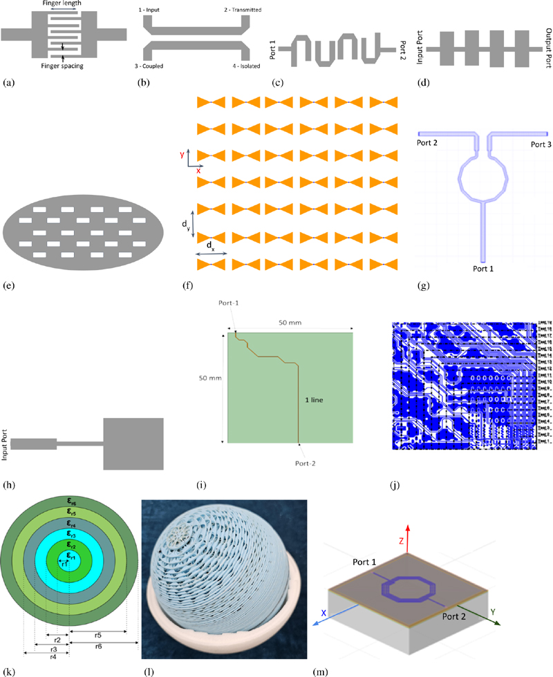
Figure 1: Various microwave circuits and antenna structures: (a) microstrip line filter, (b) microstrip directional coupler, (c) Hairpin microstrip filter, (d) four-stage bandstop filter, (e) small patch array, (f) large bow-tie patch array, (g) Wilkinson power divider, (h) patch antenna with a wideband matching circuit, (i) packaging board with a single trace, (j) typical package layer, (k) Luneburg lens cross-section, (l) 3D cutout of the interior, and (m) spiral inductor on a multilayer dielectric.
In the next section, we examine this problem and point out the difficulties encountered in generating these Green’s Functions for layered media when the operating frequency is in the millimeter frequency range. Next, we present a technique for successfully resolving the difficulties that we have identified earlier. The presentation in this section is based on a recent work by the authors and the interested reader is referred to Ozgun et al. [5] for additional details.
II. LAYERED MEDIUM GREEN’S FUNCTION FOR MILLIMETER WAVES
In this section, we introduce an efficient method for evaluating Sommerfeld integrals, which are essential in calculating spatial-domain Green’s Functions in planar multilayered media. The proposed technique effectively overcomes the challenges posed by the highly oscillatory and slowly decaying nature of these integrals, particularly at high frequencies such as millimeter waves—frequencies that are increasingly critical for advanced technologies like 5G and beyond. By employing a strategic interpolation and extrapolation scheme, the method reduces the number of sample points required to accurately represent the integrand, enabling the use of analytical integration. This simplification significantly accelerates the evaluation process. Extensive testing across various Green’s functions validates the accuracy and efficiency of the method.
Planar multilayered structures are prevalent in modern technology, with applications ranging from platform-mounted antennas to microstrip printed circuits. Accurate analysis of these structures often relies on the MoM, which is based on the Mixed-Potential Integral Equation (MPIE). A critical component of this method is the Green’s Functions, which are initially derived in the spectral domain via the Fourier transform and subsequently converted into the spatial domain through an inverse Fourier transform [6, 7]. This process results in a one-dimensional integral known as the Sommerfeld Integral (SI), defined over a semi-infinite interval of the complex spectral variable.
Evaluating these SIs is challenging due to two primary factors: (i) the presence of singularities on or near the integration path and (ii) the highly oscillatory and slowly decaying nature of the integrand. Traditional approaches often handle singularities by deforming the integration path in the complex plane, but the oscillatory behavior remains a significant obstacle. The Discrete Complex Image Method (DCIM) has been widely employed to address this issue [8]. The authors previously developed a Green’s Function module for commercial electromagnetic software using DCIM to compute SIs. While this module performed effectively at microwave frequencies, it faced substantial computational challenges at higher frequencies, such as those used in millimeter-wave applications for 5G technology. The core issue stems from the increased oscillatory nature of the SIs as the radial distance between the source and observation points becomes electrically large, a common scenario at millimeter-wave frequencies. Under these conditions, accurately representing the integrand with a few complex exponentials becomes increasingly difficult, leading to inefficiencies and numerical instability in the DCIM.
Recently, the authors introduced an innovative approach that addresses the inherent challenges of conventional DCIM [5, 9, 10]. Our method not only improves the efficiency and accuracy of SI evaluations across a broad frequency range but also simplifies the computational process without sacrificing precision. The key advancement lies in isolating the oscillatory component of the integrand as a cosine function while representing the remaining smooth envelope function using function approximation techniques such as Prony [11] or the Generalized Pencil of Function (GPOF) method [12].
A. Mathematical formulation
When simulating antennas and printed circuits on layered media using the MPIE within the MoM framework, the evaluation of SIs is critical. Solving the MPIE for a general multilayered media problem involves evaluating 16 spectral domain GFs and a total of 22 SIs [6, 7]. These SIs are expressed as:
| (1) | |
where the kernel represents the spectral-domain Green’s Function, is the Bessel function of order , is the complex spectral variable, and are the vertical coordinates of the source and observation points respectively, and is the lateral distance between these points. These parameters collectively form the foundation of this computational process.
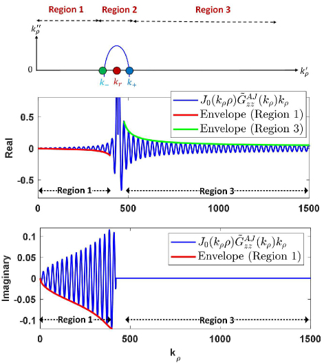
Figure 2: Illustration of the proposed integration method.
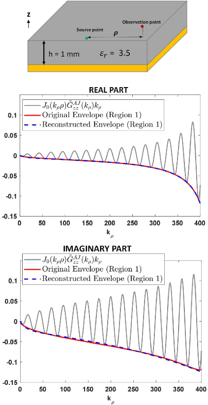
Figure 3: Original and reconstructed envelope functions in Region 1.
To address the computational challenges, our approach partitions the integration interval into multiple distinct regions (as illustrated in Fig. 2), each handled separately with a novel integration strategy that facilitates closed-form analytical solutions. In Region 2, where the singularity occurs, we deform the integration path and apply a standard numerical method to accurately manage this small but crucial region. Conversely, Regions 1 and 3, which are characterized by an oscillatory integrand due to the Bessel function, are treated differently. In these regions, the integrand behaves as a damped sinusoidal function with a smooth envelope. This behavior is effectively captured using the large-argument form of the Bessel function. Eventually, the integrand (denoted by ) is expressed as follows [5]:
| (2) |
where is the smooth envelope function, which is given by
| (3) |
where and are the poles and residues, respectively, and is the number of poles/residues.
These parameters are determined through interpolation methods such as Prony or the GPOF method. In our tests, combining the Prony method with the Total Least Squares (TLS) technique, we found that using just a few terms (e.g., or ) along with a limited number of envelope samples yielded highly accurate results. The proposed method’s ability to reduce the integrand to a few terms enables the use of straightforward closed-form analytical integration techniques. While traditional DCIM shares this feature, our method is significantly more efficient, particularly when handling the highly oscillatory integrands encountered at millimeter-wave frequencies. This increased efficiency arises because our approach focuses on the smooth envelope function rather than directly dealing with the oscillatory integrand in its original form, as done in traditional DCIM.
Figure 4: Original and reconstructed envelope functions in Region 3.
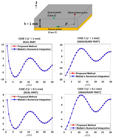
Figure 5: SI values as a function of radial distance for two different source point positions ( mm and mm) when the observation point is mm.
B. Numerical results
In this section, we present numerical examples to validate and demonstrate the effectiveness of our proposed approach. We consider a dielectric medium with a permittivity of 3.5, a loss tangent of 0.001, and a thickness of 1 mm, backed by a conducting plane, with an operating frequency of 20 GHz. The integrand corresponding to Green’s Function is analyzed, as shown in Fig. 2. Figures 3 and 4 illustrate the envelope functions, assuming a lateral distance of (where is the free-space wavelength) with the source and observation points located within the same layer ( mm, mm). It is important to note that our method is versatile and can also handle scenarios where the source and observation points are in different layers. For this example, we use terms in the summation. The envelope function is sampled and interpolated using 20 samples in Region 1 and 45 samples in Region 3. Figures 5 and 6 show the SI values as functions of the radial and vertical distances, respectively. These results are compared with those obtained using MATLAB’s numerical integration function, which is significantly more time-consuming than our method. For a single simulation in Fig. 5, the computation times on an Intel i9-10885 CPU are 1.6 seconds and 4.6 seconds using the proposed method and MATLAB’s integration routine, respectively. Similarly, for a single simulation in Fig. 6, the computation times are 0.26 seconds and 1.6 seconds using the proposed method and MATLAB’s integration routine, respectively. These results demonstrate that the proposed approach significantly accelerates the solution process, which could potentially reduce the matrix fill-time in MoM.
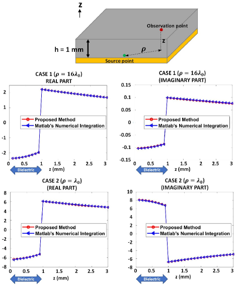
Figure 6: SI values as a function of vertical distance for two different lateral distances ( and ) when the source point is mm.
It is also worth noting that, to further enhance computational efficiency, an interpolation scheme can be employed to approximate the SI values along the vertical () direction as well. Details of this scheme can be found in [5].
III. EQUIVALENT MEDIUM APPROACH
A. EMA for printed circuits and antennas
In this section, we present a novel technique for numerical modeling of planar circuits and antennas printed on layered media, typical examples of which have been presented earlier in Fig. 1. The novelty of this approach stems from the fact that it totally obviates the need for the construction of the layered medium Green’s Function; hence, it is not only less tedious but also far more numerically efficient to use than constructing the more rigorous Green’s Function for the layered media. Although empirical, the numerical results generated by using this approach are remarkably accurate as we will see from the results for the S-parameters presented later in this section. In fact, often the difference between the S-parameter results generated by the two different commercial codes, such as CST and HFSS, is of the same order (or larger) than the difference between the numerical results derived by using the complex image method described in the previous section, and the EMA. We note that in HFSS [13], a 3D full-wave frequency-domain electromagnetic (EM) field solver utilizing the FEM is employed, while in CST [14], a time-domain EM field solver based on the FDTD method isused.
The basic strategy of the EMA is relatively simple. We begin with a planar transmission line, such as a microstrip line, printed on a substrate (typically a single-layer dielectric) backed by a ground plane, as shown in Fig. 6 (a). Next, we replace the layered medium with a homogeneous medium in the entire half-space above the ground plane, as shown in Fig. 6 (b). The effective epsilon () of the homogeneous medium is obtained by using the equations (4)-(8) that were originally derived in [15], for a microstrip line whose trace width is , substrate thickness is , and whose relative permittivity of the substrate is . Our strategy is to use these effective epsilons to replace the original geometries of the microstrip circuits and antennas with their equivalent geometries (see Figs. 6 (a) and 6 (b)). Another reliable way of doing this is to determine of the homogeneous medium such that the propagation constant along the original microstrip line in Fig. 6 (a) is the same as that of the transmission line shown in Fig. 6 (b), which is embedded in a homogeneous half-space.
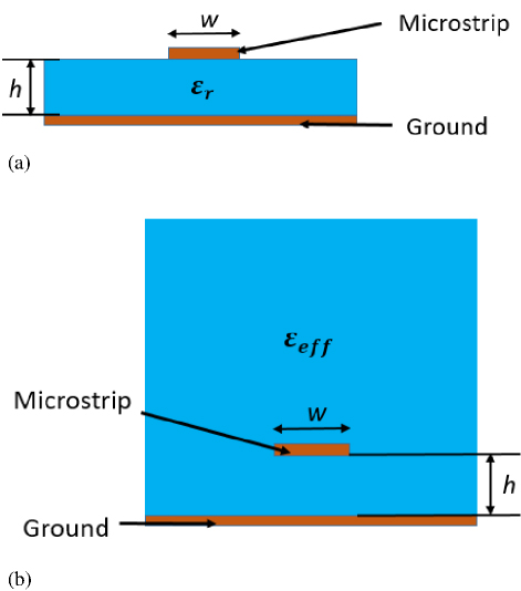
Figure 7: Comparison of the original geometry in a layered medium and the equivalent geometry in a homogeneous medium: (a) side view of the original geometry with free space above the patch and a dielectric substrate below and (b) side view of the equivalent geometry with an equivalent dielectric above and below the patch.
We present two options for determining the . The first of these is to use the quasi-analytical formulas given in [15], which express the effective epsilon directly in terms of the parameters of the transmission line shown in Fig. 7. The formulas are given in equations(4)-(8):
| (4) |
| (5) |
| (6) |
| (7) |
| (8) |
where is width of the microstrip, is thickness of the substrate, is the speed of light in vacuum, is the frequency of operation, is dielectric constant of the substrate in Fig. 6 (a), is equivalent dielectric constant of the homogeneous medium of the half-space in Fig. 6 (b). The second option, referred to herein as the short-circuit method, first terminates the line with a short circuit and then extracts the wave number from the resulting standing waves on the line by measuring the distance between the minima of the standing waves. The latter approach is more accurate but is also more time-consuming because it requires a numerical simulation of the microstrip transmission line. In any case, the two results for the are very close to each other.
Let us consider an example to illustrate the extraction procedure of the effective epsilon (). We begin with an original geometry of a microstrip line whose width is 4.84 mm, the relative permittivity () of its substrate is 2.2, while its thickness is 1.57 mm. The first method, based on the formula given in equations (4)-(8), provides = 1.89, at the frequency of interest 2.4 GHz. The second method, based on short circuit termination, yields = 1.9, for which the propagation constant ( rad/m) of the line embedded in a homogeneous medium is identical to the propagation constant ( rad/m) of the original line in a layered medium at the frequency of 2.4 GHz. We observe that both the methods are reliable and accurate, and we subsequently use the simpler ‘equivalent’ geometry to model the microstrip circuit, which obviates the need for the construction of the layered medium Green’s Function altogether; hence the EMA is numericallyefficient.
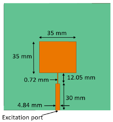
Figure 8: Top view of the geometry of MPA (backed by full ground plane). The green area shows substrate and the orange area shows copper.
Next, we proceed to illustrate the use of the EMA by considering the example of a microstrip patch antenna (MPA) fed by a stepped transmission line geometry designed to provide the antenna with a wideband match. The antenna configuration is shown in Fig. 8. The relative permittivity () of the substrate is 2.2, and its thickness () is 1.57 mm. The reason we choose this example is that the width () of the trace in this geometry changes three different times; hence, it brings up an important question that we must resolve before proceeding to simulate this geometry, regardless of which method we use–the formula or the short-circuit termination–to extract the effective epsilon (). Since this geometry has three different widths, we would generate three different values for the , two for the two transmission lines with different trace widths, and the third for the patch, which we are still treating as a microstrip line for the purpose of extracting the . The quasi-analytical formulas, given in equations (4)-(8) generated three different values for the viz., 1.73, 1.89, and 2.14 for the three trace widths, = 0.72 mm, 4.84 mm, and 35 mm, respectively, at the frequency of interest 5.5 GHz. (Note: We can apply the same procedure for other frequencies of interest equally well.) The problem is that an MoM code can only deal with a single , and not with different epsilons in different sub-regions. To address this issue, we propose two different approaches.
In the first approach, we define a composite representation of the as a weighted average which reads:
| (9) |
| (10) |
where represents the area of the patch ( = 35 mm), corresponds to the area of the thin line ( = 0.72 mm), and denotes the area of the feed line ( = 4.84 mm). The effective permittivities associated with these regions are denoted as for the patch, for the thin line, and for the feed line. Using equation (9), the composite effective permittivity is computed as 2.11.
This composite is then used to simulate the antenna, including both the patch and its stepped feedline, and the results are compared with those obtained from a commercial solver for the original layered-medium geometry. Figure 9 presents this comparison, showing the S-parameter () of the antenna as a function of frequency, derived using the HFSS simulator. The results indicate a slight shift in the resonant frequency of the antenna when employing the numerical simulation based on the EMA, using the HFSS simulation as the reference.
To further improve the agreement between the two methods, an empirical factor is introduced (see equation (10)), which scales down the composite to 2.02. Through numerical experiments, is determined to be 0.96. Figure 9 illustrates that the plot of the original MPA in a layered medium (substrate permittivity =2.2) closely matches the plot of the equivalent MPA geometry when the modified composite is set to 2.02. The S-parameter results obtained using this adjusted composite permittivity demonstrate the effectiveness of the empirical factor in enhancing the accuracy of the EMA. The agreement achieved through this correction is often comparable to or even better than that obtained by using two different commercial solvers to simulate the same problem geometry.
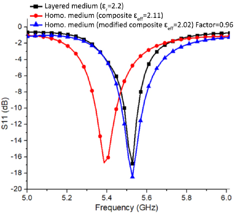
Figure 9: Comparison plot of versus frequency for the MPA geometry between layered medium and homogeneous medium. Terminating impedance, = 50 for both mediums. The simulator used: HFSS.
It is evident that indeed using a modified composite yields a result that compares very favorably with the one obtained from a rigorous numerical simulation that employs a commercial code such as the HFSS or CST, for instance, and its use provides an obvious time-saving advantage. We now present two other examples to demonstrate the versatility of the EMA utilizing the formula method to derive the effective epsilon of the equivalent geometry of the problem at hand. As an example, we show the results of the geometry of four elements MPA utilizing, as shown in Fig. 10, for the frequency range 2 – 3 GHz. The relative permittivity () of the substrate is 2.2 in a layered medium, and its thickness () is 1.57 mm. The composite of the homogeneous medium is calculated to be 2.11 and the empirical factor, as 0.97, scales down the composite to 2.05. The comparison is shown in Fig. 11, which plots the S-parameter () of the antenna array as a function of frequency, using HFSS, at the frequency of interest 2.4 GHz. We observe that the plot of the original MPA array in a layered medium (substrate = 2.2) matches well with the plot of the equivalent geometry of the MPA array in a homogeneous medium, when the modified composite of the homogeneous medium is 2.05.
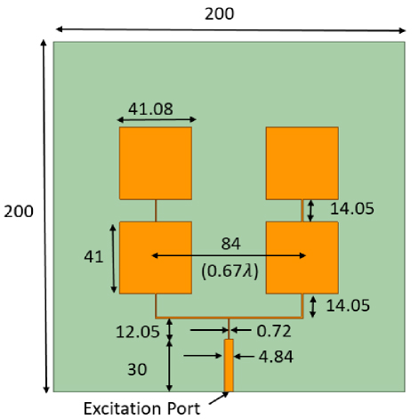
Figure 10: Top view of the geometry of four elements MPA array (backed by full ground plane). All dimensions are in millimeters (mm). The green area shows substrate and the orange area shows copper.
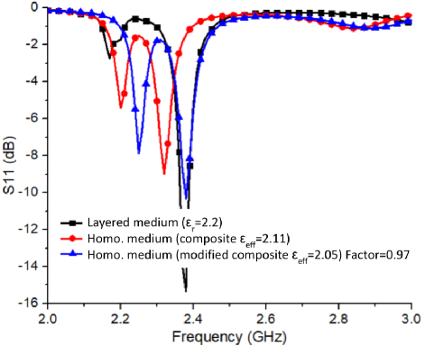
Figure 11: Comparison of as a function of frequency for the MPA array geometry in both layered and homogeneous media. The terminating impedance is 50 in both cases. Simulations were performed using HFSS.
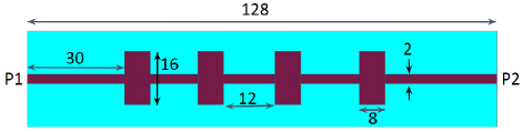
Figure 12: Top view of the geometry of stepped filter (backed by full ground plane). All dimensions are in millimeters (mm). The green area shows substrate and the brown area shows copper.
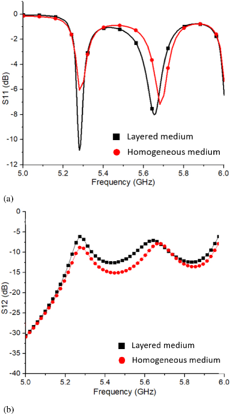
Figure 13: Comparison of S-parameters as a function of frequency for the stepped filter geometry in both layered and homogeneous media: (a) , (b) . The terminating impedance is 50 in both cases. Simulations were performed using HFSS.
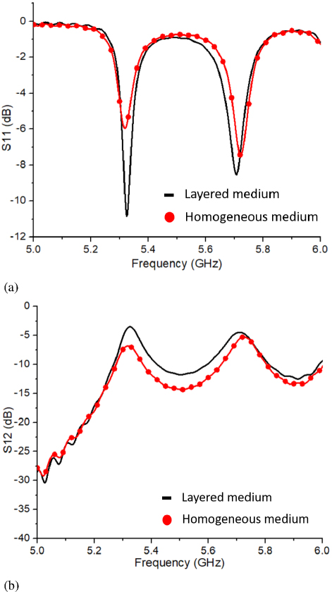
Figure 14: Comparison of S-parameters as a function of frequency for the stepped filter geometry in both layered and homogeneous media: (a) , (b) . The terminating impedance is 50 in both cases. Simulations were performed using CST.
Next, we present the results for the two-port stepped filter geometry, shown in Fig. 12, for the frequency range 5–6 GHz. The relative permittivity () of the substrate is 4.0, and its thickness () is 1 mm. Figures 13 and 14 plot the S-parameters (, ) as functions of frequency obtained by using the HFSS and CST. The S-parameters plots of the original geometry of the stepped filter in a layered medium (substrates = 4.0) match with the S-parameters plot of the equivalent geometry of the stepped filter embedded in a homogeneous medium, at the frequency of interest 5.5 GHz; when the modified composite of the homogeneous medium is 3.25.
It is worthwhile to mention here that although we have only presented results based on the use of the ‘formulas’ to obtain the effective epsilons of the microstrip lines, we could have also employed the short-circuit termination method with a slightly different empirical factor to achieve essentially the same S-parameter results for the problem at hand that agree with the reference results for the same parameters when the simulation is carried out by using the commercial CEM codes. As mentioned before, the ‘formula’ option is more efficient and, hence, is our preferred choice.
Before closing this section, we would like to mention a novel strategy, which enables us to use multiple effective , as opposed to a single composite one, by combining the EMA with the T-matrix approach. This approach begins with a domain decomposition of the original geometry into several blocks, each of which has its own effective that depends on the width of the trace as we have explained earlier. The next step is to extract the S-parameters of each of these blocks by using the EMA. Finally, we generate the S-parameters of the original geometry by cascading the S-parameters of the different blocks by using the T-matrix algorithm [16]. This algorithm will be discussed more fully in section IV., where hybrid CEM methods with finite methods will be presented.
To illustrate the proposed procedure for handling geometries with multiple trace widths, let us consider the case of double-step discontinuity in a microstrip line, shown in Fig. 15. The three blocks for this microstrip line geometry are shown in Fig. 15 printed on a substrate = 4 of thickness 1.5mm. The Line-1, length = 25mm, width = 2.4mm, Line-2, length = 25mm, width = 0.4mm, and Line-3, length = 25mm, width = 2.4mm. Note that the S-parameters of the individual blocks, each of which in this example is a simple uniform transmission line, can be readily derived on paper without having to run any numerical simulation at all. We have verified that the accuracy of this approach is very high, as the numerical results to be presented in section I [17] readily demonstrate.
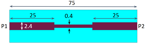
Figure 15: A discontinuous microstrip line. All dimensions are in millimeters (mm).
A similar strategy can be used to simulate the packaging problem shown in Figs. 0 (i) and 0 (j).
B. Equivalent medium approach for metasurfaces and metamaterials
In recent years, there has been an increase in the use of metamaterials (MTMs) and metasurfaces (MTSs) as performance enhancers of communication antennas. Typically, MTMs and MTSs are truncated periodic or quasi-periodic structures, designed to control the reflection, transmission, or propagation characteristics of a material slab (or a surface) in a desirable manner. However, an extensive search of the literature reveals that very rarely we are provided a clue that explains how to choose the particular shape, size, or material parameters of an element of the quasi-periodic MTS to realize the desired performance of the antenna utilizing the MTS. Designing the MTS typically requires extensive numerical simulations, which can be tedious as well as time-consuming, especially when the antenna, which is typically an array for millimeter wave applications, is several wavelengths in size.
A common strategy for dealing with MTSs is to extract their material parameters, as a first step to numerically modeling them. A number of authors [15, 18, 19, 20] have presented techniques for extracting the material parameters () of the unit cell of an MTM slab. The present technique differs from the existing methods for characterizing MTMs and MTSs in two ways. First, it works with -only parameters, by assuming that is either or constant. Second, it extracts the parameters of the tensor in a very different way than has been published in the existing literature. The method of extraction proposed herein is not only simple but is also tailored for typical antenna applications, which depend upon the reflection, transmission, and propagation characteristics of MTSs, for instance.
In the previous section, we have presented the details of the EMA for efficient numerical simulation of microstrip circuits and antennas bypassing the generation of Green’s Function for layered media. Computational bottleneck also arises when dealing with MTSs and MTMs, in combination with antennas, used to enhance the performance of the antenna or to realize the antenna itself by employing MTMs because the requisite material is unavailable off-the-shelf.
The basic strategy is still to replace the metamaterial – which often has fine or multi-scale features – with an equivalent dielectric, which is much simpler to deal with numerically. The use of this tactic renders the simulation numerical simulation much more efficient than it would be if we were to deal with the original MTM directly, as we would when using a commercial EM simulator. In this section, we provide the details of this procedure, based on the EMA by considering the example of a MPA (or array) covered with an MTS superstrate to enhance its performance.
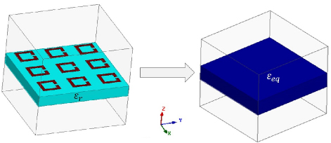
Figure 16: Original MTS (left) and its equivalent dielectric slab (right).
The EMA to deriving the equivalent dielectric slab is based on matching the phase of the transmission coefficient of the original metasurface and the equivalent dielectric slab based in a unit cell, as shown in Fig. 16.
The first step in this EMA-based procedure is to replace the unit cell of the metasurface with a permittivity tensor by using the procedure described below. The procedure is general and is applicable to both isotropic and anisotropic metasurfaces.
By using this approach, we can calculate the of the metasurfaces in each direction of propagation. Generally, the metasurface is an anisotropic slab and is characterized by using an tensor as follows:
| (11) |
where , , and are the three propagation directions.
After deriving the equivalent epsilon () representation of the original metasurface, we replace it just by the dielectric slab for the numerical simulation of the antenna plus metasurface combination.
For an example of MTS material (shown in Fig. 16 (a)), the diagonal elements in the above matrix are identical for and directions and the of the dielectric slab can be represented by:
| (12) |
However, the equivalent epsilon of the dielectric slab for the MTS in Fig. 16 (b), is represented by a uniaxial representation (13):
| (13) |
where the and are not the same.
For certain anisotropic materials, we only need the diagonal matrix to characterize the permittivity of the material, but for accurately characterizing a chiral material [21], we need to include the off-diagonal terms of the tensor as well. Figure 16 (c) shows the layout of the example unit cell of a chiral metasurface, for which the for the anisotropic off-diagonal matrix is represented by:
| (14) |
Figure 17: Geometries of the example unit cells: (a) MTS material, (b) anisotropic MTS, and (c) chiral MTS.
It is worthwhile to mention here that the EMA is very versatile. It is not just limited in its application to planar circuits, examples of which have been presented in Fig. 1, but also to other non-planar and inhomogeneous geometries to efficiently simulate other types of geometries such as Luneburg lenses fabricated by using artificial dielectrics (see Figs. 0 (k) and 0 (l)), and spiral inductors printed on multi-layer substrates, shown in Fig. 0 (m). Numerically modeling lens is very time-consuming, especially when the lens diameter is several wavelengths, as it typically is for millimeter wave applications, and the lens is fabricated by using artificial dielectrics as shown in Fig. 0 (l). Similarly, numerically simulating the inductor to extract its circuit parameters is very time-consuming as well as memory-intensive, because the thicknesses of the dielectric layers are very small – in the micron range – which calls for the use of a very fine mesh to represent the geometry under consideration accurately. However, we can obviate this problem by replacing the multi-layered dielectric with one (or two) layers of moderate thickness, thus rendering the problem very manageable from the numerical simulation point of view.
Additionally, the method is well suited for hybridizing the Integral equation and finite method by using a novel approach which overcomes the roadblock presented by the fact that the MoM deals with induced currents whereas the finite methods work with fields, making the problem of merging the two algorithms to handle a given problem very challenging indeed.
In summary, we have presented the EMA in this section which is very powerful as well as versatile, and, hence, is a very useful tool for numerical simulation of a wide class of problems.
C. Application of EMA to metasurfaces-basedantennas
Next, we explain how we use the EMA to first characterize the MTS, and then simulate an antenna (or an array) that utilizes the MTS as a superstrate to enhance its performance, such as its gain. The simulation time for such an antenna plus superstrate combination can be very long when the operating frequency is in the millimeter wave range. Our goal is to replace the original MTS, shown in Fig. 17 (a).
To demonstrate the efficacy of the proposed method, we compare the CPU times and memory burdens when we simulate an array of three microstrip patches covered by a metasurface superstrate, shown in Fig. 17 (a), versus when the superstrate is replaced by an isotropic dielectric as shown in Fig. 17 (b). The dielectric constant of the material and the FSS thickness are, respectively, 17 and 0.6mm, while the remaining dimensions of the unit cell of the MTS Superstrate are shown in Fig. 19.
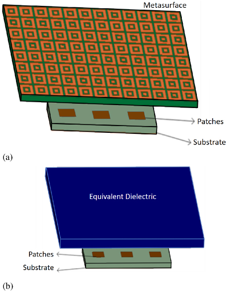
Figure 18: Three-element MPA with different superstrates: (a) metasurface superstrate and (b) equivalent dielectric.
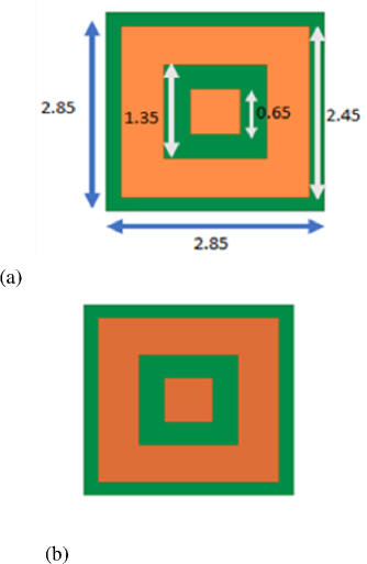
Figure 19: Dimensions of the unit cell of the MTS superstrate presented in Fig. 18: (a) top view and (b) bottom view.
Table 1 presents the comparison time and memory requirement for the patch array covered with metasurfaces and with equivalent dielectric. We observe a relevant reduction in the utilized RAM and in the CPU time by using the EMA. The CPU time simulation and the RAM requirement are reduced by a factor of 5 and 5.5, respectively. The advantage of using the EMA over a direct simulation of the original geometry comprising of the antenna array and the MTS superstrate is clearly evident from Table 1.
Table 1: Comparison of CPU runtimes and required RAM values for the Equivalent Medium approach and the original array covered with the metasurface superstrates (Fig. 18)
| Design | Max RAM (GB) |
Real Time (hh:mm:ss) |
CPU Time (hh:mm:ss) |
| Three-element patch | 1.04 | 0:14:04 | 0:13:59 |
| Three element patch+Metasurface | 91.3 | 72:55:04 | 95:51:09 |
| Three element patch+Equivalent Dielectric | 24.4 | 14:56:47 | 16:57:22 |
IV. THE T-MATRIX APPROACH FOR CASCADED TWO-PORT NETWORKS
In this section, we present the T-matrix approach to show how to use it in conjunction with the domain decomposition technique to handle a wide variety of printed circuits and antenna geometries, illustrated in Fig. 10 in section III., in a numerically efficient manner.
We start by choosing the geometry of an open-ended stub in a microstrip line, and dividing the original problem into three blocks, as shown in Fig. 20, to detail the T–matrix procedure. The relevant equations for deriving the S-parameters of the original geometry, by utilizing the S-parameters of the three blocks in which the geometry is subdivided, are given below:
| (15) |
where the starting parameters are for the three blocks and the parameters are for the total stub line. The details of the principle of the T-matrix approach were discussed in section III., part A..
Figure 20: Example of a stub divided into three blocks.
One of the 3D geometries, shown in Fig. 21, is a via, which connects transmission lines from the top to the bottom layer by using the through-hole via. This problem is not amenable to convenient simulation using integral equation methods, not only because of the 3D nature of its geometry but also because it is difficult to construct Green’s Function for the region in the neighborhood of the through–hole via. However, the T-matrix approach, presented in this section, enables us to handle this problem by using a hybrid algorithm comprised of a combination of finite methods, such as the FEM or FDTD, and integral equation techniques based on the Green’s Function that we have discussed previously in section III.. The hybrid method is not only powerful and versatile, but it is also numerically more efficient than either the finite method or the integral-equation-based approach when directly applied to the problem at hand, namely the through-hole via with microstrip feed lines printed on top and bottom layers of the configuration.
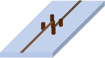
Figure 21: Example of 3D geometry.
Although not included here, the method has been thoroughly tested and proven to be accurate when applied to a wide variety of problems, including not only planar circuits but also 3D and 2D circuits, as well as antennas, such as those shown in Fig. 22. The MPA arrays with a corporate feed, described in Fig. 22, have the following dimensions and substrate parameters: L = 10.08 mm, W = 11.79 mm, d = 1.3 mm, d = 3:93 mm, L1 = 12:32 mm, L2 = 18.48 mm, D1 = 23.58 mm, D2 = 22.40 mm, =2.2, d=1.59mm, operating at 9.13 GHz. The T-junction is handled separately using the circuit method.
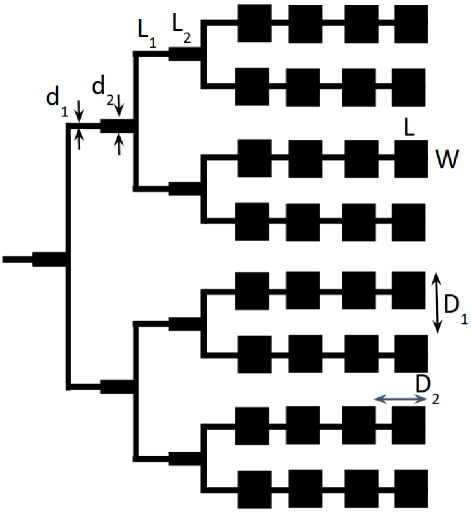
Figure 22: Microstrip patch antenna array.
In summary, in this section we have presented the EMA which is very powerful as well as versatile, and, hence, is a very useful tool for a wide class of problems. In Part-II [17] of this paper we will go on to discuss three other strategies for performance enhancement of CEM techniques, viz., Characteristic Basis Function Method (CBFM), Mesh Truncation for Finite Methods by using a new form of the Perfectly Matched Layer (PML), and GPU acceleration of MoM as well as FDTDalgorithms.
ACKNOWLEDGMENT
The authors acknowledge their team members and research collaborators, including Chao Li, Donia Ouesleti, Koushik Dutta, Yang Su, and others for their contributions and helpful discussions. We thank Dr. Danie Ludick for pointing us to the “cemagg/SUN-EM” GitHub library, which was used to parse FEKO’s MoM-based data into MATLAB. We also acknowledge the use of ChatGPT, developed by OpenAI, for assistance in text editing during the preparation of this manuscript. The tool was used solely to improve clarity and language, without contributing to the scientific content of the paper.
REFERENCES
[1] R. F. Harrington, Field Computation by Moment Methods. New York, NY: Wiley-IEEE Press,1993.
[2] P. P. Silvester and R. L. Ferrari, Finite Elements for Electrical Engineers. Cambridge: Cambridge University Press, 1996.
[3] K. S. Yee and J. S. Chen, “The finite-difference time-domain (FDTD) and the finite-volume time-domain (FVTD) methods in solving Maxwell’s equations,” IEEE Transactions on Antennas and Propagation, vol. 45, no. 3, pp. 354-363,1997.
[4] T. Hagstrom and H. Keller, “Asymptotic boundary conditions and numerical methods for nonlinear elliptic problems on unbounded domains,” Mathematics of Computation, vol. 48, no. 178, pp. 449-470, 1987.
[5] O. Ozgun, R. Mittra, and M. Kuzuoglu, “An efficient numerical approach for evaluating Sommerfeld integrals arising in the construction of Green’s functions for layered media,” IEEE J. Multiscale Multiphys. Comput. Tech., vol. 7, pp. 328-335, 2022.
[6] K. Michalski and D. Zheng, “Electromagnetic scattering and radiation by surfaces of arbitrary shape in layered media. I. Theory,” IEEE Trans. Antennas Propag., vol. 38, no. 3, pp. 335-344, 1990.
[7] P. Yla-Oijala and M. Taskinen, “Efficient formulation of closed-form Green’s functions for general electric and magnetic sources in multilayered media,” IEEE Trans. Antennas Propag., vol. 51, no. 8, pp. 2106-2115, 2003.
[8] Y. Mengtao, T. Sarkar, and M. Salazar-Palma, “A direct discrete complex image method from the closed-form Green’s functions in multilayered media,” IEEE Trans. Microw. Theory Tech., vol. 54, no. 3, pp. 1025-1032, 2006.
[9] R. Mittra, O. Ozgun, C. Li, and M. Kuzuoglu, “Efficient computation of Green’s functions for multilayer media in the context of 5G applications,” in 2021 15th European Conference on Antennas and Propagation (EuCAP), pp. 1-5, 2021.
[10] O. Ozgun, C. Li, M. Kuzuoglu, and R. Mittra, “An efficient approach for evaluation of multilayered media Green’s functions,” in 2021 IEEE International Symposium on Antennas and Propagation and USNC-URSI Radio Science Meeting (APS/URSI), pp. 1107-1108, 2021.
[11] A. Fernandez Rodriguez, L. de Santiago Rodrigo, E. Lopez Guillen, J. M. Rodriguez Ascariz, J. M. M. Jimenez, and L. Boquete, “Coding Prony’s method in MATLAB and applying it to biomedical signal filtering,” BMC Bioinformatics, vol. 19, no. 451, 2018.
[12] Y. Hua and T. Sarkar, “Generalized pencil-of-function method for extracting poles of an EM system from its transient response,” IEEE Trans. Antennas Propag., vol. 37, no. 2, pp. 229-234, 1989.
[13] Ansys Corporation. (2024). ANSYS HFSS, high-frequency electromagnetic field simulation software [Online]. Available: https://www.ansys.com
[14] Dassault Systèmes. (2024). CST Studio Suite, electromagnetic field simulation software [Online]. Available: https://www.3ds.com
[15] D. Smith, D. Vier, T. Koschny, and C. Soukoulis, “Electromagnetic parameter retrieval from inhomogeneous metamaterials,” Physical Review E—Statistical, Nonlinear, and Soft Matter Physics, vol. 71, no. 3, p. 036617, 2005.
[16] P. C. Waterman, “Matrix formulation of electromagnetic scattering,” Proceedings of the IEEE, vol. 53, no. 8, pp. 805-812, 1965.
[17] R. Mittra, T. Marinovic, O. Ozgun, S. Liu, and R. K. Arya, “Novel strategies for efficient computational electromagnetic (CEM) simulation of microstrip circuits, antennas, arrays and metamaterials Part-II: Characteristic basis function method, perfectly matched layer, GPU acceleration,” Applied Computational Electromagnetics Society (ACES) Journal, pp. 000-000, 2025.
[18] A. B. Numan and M. S. Sharawi, “Extraction of material parameters for metamaterials using a full-wave simulator [education column],” IEEE Antennas and Propagation Magazine, vol. 55, no. 5, pp. 202-211, 2013.
[19] T. A. Elwi, M. M. Hamed, Z. Abbas, and M. A. Elwi, “On the performance of the 2D planar metamaterial structure,” AEU-International Journal of Electronics and Communications, vol. 68, no. 9, pp. 846-850, 2014.
[20] M. R. Benson, A. G. Knisely, M. A. Marciniak, M. D. Seal, and A. Urbas, “Permittivity and permeability tensor extraction technique for arbitrary anisotropic materials,” IEEE Photonics Journal, vol. 7, no. 3, pp. 1-13, 2015.
[21] A. Yahyaoui and H. Rmili, “Chiral all-dielectric metasurface based on elliptic resonators with circular dichroism behavior,” International Journal of Antennas and Propagation, vol. 2018, no. 1, p. 6352418, 2018.
BIOGRAPHIES

Raj Mittra is a Professor in the Department of Electrical and Computer Engineering of the University of Central Florida in Orlando, FL., where he is the Director of the Electromagnetic Communication Laboratory. Before joining the University of Central Florida, he worked at Penn State as a Professor in the Electrical and Computer Engineering from 1996 through June 2015. He was a Professor in the Electrical and Computer Engineering at the University of Illinois in Urbana-Champaign from 1957 through 1996, when he moved to Penn State University. Currently, he also holds the position of Hi-Ci Professor at King Abdulaziz University in Saudi Arabia and a Visiting Distinguished Professor in Zhongshan Institute of CUST, China. He is a Life Fellow of the IEEE, a Past-President of AP-S, and has served as the Editor of the Transactions of the Antennas and Propagation Society. He won the Guggenheim Fellowship Award in 1965, the IEEE Centennial Medal in 1984, and the IEEE Millennium Medal in 2000. Other honors include the IEEE/AP-S Distinguished Achievement Award in 2002, the Chen-To Tai Education Award in 2004 and the IEEE Electromagnetics Award in 2006, and the IEEE James H. Mulligan Award in 2011. He has also been recognized by the IEEE with an Alexander Graham Bell award from the IEEE Foundation.

Ozlem Ozgun is currently a full professor in the Department of Electrical and Electronics Engineering at Hacettepe University, Ankara, Turkey. She received her B.Sc. and M.Sc. degrees from Bilkent University and her Ph.D. from Middle East Technical University (METU), all in Electrical and Electronics Engineering. She was a postdoctoral researcher at Penn State University, USA. Her research focuses on computational electromagnetics and radiowave propagation, including numerical methods, domain decomposition, transformation electromagnetics, and stochastic electromagnetic problems. Dr. Ozgun is a Senior Member of IEEE and URSI and a past chair of the URSI Turkey steering committee. She has been selected as a Distinguished Lecturer (DL) by the IEEE Antennas and Propagation Society (AP-S) for the period of 2025-2027. Her awards include the METU Best Ph.D. Thesis Award (2007), the Felsen Fund Excellence in Electromagnetics Award (2009), and the IEEE AP-S Outstanding Reviewer Award (2023-2024). She was recognized among the world’s top 2% most influential scientists (Stanford University & Elsevier, 2023–2024) and received the Hacettepe University 2024 Science Award.

Vikrant Kaim (Member, IEEE) received the Ph.D. degree in electronics and communication from the Jawaharlal Nehru University, Delhi, India, in 2022. He was a Postdoctoral Fellow with the Department of Electrical and Computer Engineering, University of Alberta, Edmonton, Canada, from January 2003 to December 2023. In December 2023, he joined the Department of Electronics and Communication Engineering as an Assistant Professor at the Faculty of Technology, University of Delhi, Delhi, India. Since Dec. 2024, he has been working as an Assistant Professor at the Centre for Research in Electronics (CARE), Indian Institute of Technology Delhi (IIT Delhi). His research interests include applied electromagnetics with focus on bio-electromagnetics and biomedical devices for wearable, implantable and ingestible applications such as wireless power transfer, retinal prosthesis, cardiac implants, and capsule endoscopy. Mr. Kaim was a recipient of the prestigious CSIR Senior Research Fellowship in 2019. He has authored/co-authored 26 publications in reputed international journals and conferences. He is also credited with 3 Indian patents. He is serving as a reviewer for the IEEE Transactions on Antennas and Propagation, IEEE Transactions on Microwave Theory and Techniques, and IEEE Transactions on BiomedicalEngineering.

Abdelkhalek Nasri received the B.Sc. degree in electronic systems and the Ph.D. degree in electronics from the Faculty of Sciences of Tunis, Tunisia, in 2011 and 2017, respectively. He is currently a Postdoctoral Fellow at XLIM in Limoges, France. From 2021 to 2022, he was a Research Scholar at the University of Central Florida, Orlando, FL, USA. His research interests include antennas, phased arrays, frequency-selective surfaces, substrate-integrated waveguides, scattering of electromagnetic waves, and bioelectromagnetics.

Prashant Chaudhary received his B.Sc. (Honors) in Electronics, followed by an M.Sc. in Electronics, and a Ph.D. from the University of Delhi, Delhi, India. He is currently a research assistant in the Department of Electrical and Computer Engineering (ECE) at the University of Central Florida, USA. His research interests include planar antennas, MIMO (Multiple Input Multiple Output) systems, circularly polarized antennas, 5G communication technology, metasurfaces, magnetic substrates, and metamaterials. He has published over 15 research papers in journals and conferences.

Ravi K. Arya is a Distinguished Professor and Director of the Xiangshan Laboratory Wireless Group at the Zhongshan Institute of Changchun University of Science and Technology (ZICUST), China. He earned his Ph.D. in Electrical Engineering from Pennsylvania State University, USA, under the supervision of Prof. Raj Mittra, following an M.Tech in RF and Microwave Engineering from the Indian Institute of Technology (IIT) Kharagpur (advised by Prof. Ramesh Garg) and a B.Tech from Delhi Technological University, India. With a career spanning both academia and industry, Dr. Arya has held positions at ECIL (India), C-DOT (India), Ansys Inc. (USA), and ALL.SPACE (USA), as well as academic roles at NIT Delhi (India) and JNU (India). He has authored over 90 peer-reviewed publications, seven book chapters, and four patents. His research focuses on antenna design, computational electromagnetics, machine learning applications in electromagnetics, and RF system modeling.
ACES JOURNAL, Vol. 40, No. 5, 373–389
doi: 10.13052/2025.ACES.J.400501
© 2025 River Publishers