Cross-Coupled Wide Stopband SIW Bandpass FilterLoading Snake-shaped Slot
Yawen He, Zhonghua Ma, Mengnan Wang, Jingyao Huang, and Yanfeng Jiang
1School of Marine Information Engineering
Jimei University, Xiamen 361021, China
yw_he@jmu.edu.cn, mzhxm@jmu.edu.cn, 202211810012@jmu.edu.cn, 202321303073@jmu.edu.cn
2College of IoT Engineering
Jiangnan University, Wuxi 214122, China
jiangyf@jiangnan.edu.cn
*Corresponding authors: Zhonghua Ma (mzhxm@jmu.edu.cn); Yanfeng Jiang (jiangyf@jiangnan.edu.cn)
Submitted On: December 6, 2024; Accepted On: April 2, 2025
ABSTRACT
In this paper, a novel fourth-order bandpass filter is proposed and fulfilled, which is based on a cross-coupling structure achieved by etching snake-shaped slots between vias of adjacent SIW cavities. The gap of the vias’ wall between adjacent SIW cavities is used to achieve coupling between the two cavities. The length of the coupling gap can be adjusted to change the resonant frequency of TE mode to TE mode. The offset distance between the ports and the centerline is disclosed as a key parameter to suppress undesired modes, achieving wide stopband characteristics. The snake-shaped slot is loaded on the vias’ wall between SIW cavities for the enhancement of the electrical coupling, which produces a pair of transmission zeros (TZs) on either side of the passband, enhancing frequency selectivity. The filter design is validated through simulation, fabrication, and measurement of a fourth-order SIW filter with TZs. It is verified that the designed filter shows promising characteristics, with a center frequency of 24.1 GHz, an insertion loss of 0.52 dB, and a return loss exceeding 11.8 dB. It is observed that two TZs appear at 22.82 GHz and 25.15 GHz, respectively, each exhibiting a suppression level better than 20 dB. The designed filter shows potential applications in microwave and radio frequency circuits, as well as in wireless communication systems.
Index Terms: Bandpass filter, cross-coupling, transmission zeros, wide stopband.
I. INTRODUCTION
The rapid development of wireless communication systems accelerates the demand for compact, high-performance, multi-band filters. Modern communication systems, such as 5G, 6G, Internet of Things (IoTs), and satellite communication, are associated with increasingly high-performance requirements for the filter. In particular, for high-frequency signal transmission, filters with low insertion loss, high selectivity, and good out-of-band rejection play a key role in the system. Substrate Integrated Waveguide (SIW) has emerged as an ideal choice for designing high-end filters due to its advantages such as low cost, low loss, small size, high Q-factor, and seamless integration with other planar microwave circuits [1–3]. Recently, various SIW filters with different topologies and filtering characteristics have been proposed [4, 5]. To achieve sharp frequency selectivity, transmission zeros (TZs) must be inserted on both sides of the filter’s passband [6–8]. Extensive research has been conducted in the community on the SIW filter, exploring different geometries and coupling mechanisms to realize TZs. However, limitations are still faced in balancing high selectivity and low insertion loss.
In current methods, additional structures are typically etched on the top layer of the SIW cavity to form mixed coupling of electric and magnetic fields, thereby introducing TZs on both sides of the passband in bandpass filters [9]. However, the adoption of these hybrid SIW structures may deteriorate the integrity and the shielding effectiveness of SIW cavities, potentially increasing radiation losses. Although electrical coupling is provided by the slot-line structure of the cascaded SIW cavities, and it can also be used as resonators, the circuit size of the filter is reduced simultaneously [10–16]. However, it should be noted that the design of these slot-line structures is very complex and could seriously interfere with the surface current distribution.
To overcome these challenges, attempts have been made to achieve multi-mode SIW filters by introducing metallized via perturbations [17–20]. However, parasitic capacitance and inductance are introduced inevitably by the vias. These parasitic effects would cause changes in the distribution of the electromagnetic fields, which affect the frequency response of the filter. The resonance frequency would be shifted, and the bandwidth would be narrowed due to these parasitic effects. The influences would be more severe at microwave and radio frequency. In multi-layer SIW filters, the vertically stacked circuit structure shows more flexible options for implementing electrical coupling [21]. However, production costs are increased, and circuit layout flexibility is limited by the complexity of designing and manufacturing multilayer structures. Therefore, a solution that can provide effective out-of-band suppression and low insertion loss is urgently needed to keep the filter’s shielding effectiveness and to simplify its multi-layer structure.
The design of SIW-based filters generally faces several challenges, including the balance between low insertion loss and high manufacturing complexity, as well as the impact of parasitic effects on performance. To address these issues, a novel filter design is proposed in this paper, which combines serpentine slots with optimized via configurations. The serpentine slot design is simple and maintains continuous working currents on the surface, effectively enhancing the filter’s performance. By introducing the serpentine slot design based on a single-layer PCB structure, cross-coupling is successfully achieved, and TZs are introduced on both sides of the passband, effectively suppressing higher-order frequencies.
In [22], a design approach is reported where the coupling slot width of a SIW filter is adjusted to achieve flexible coupling. Through this method, a TZ is introduced in a half-mode SIW filter, and a bandpass filter is successfully constructed by integrating SIW and half-mode SIW (HMSIW) structures. However, while this design optimizes in-band filter performance, it does not effectively suppress higher-order modes, leading to spectral leakage and undesired resonances at higher frequencies. In modern millimeter-wave systems, unsuppressed higher-order modes cause severe interference in densely packed frequency bands, degrading signal integrity and system performance. This limitation underscores the need for novel filter designs that enhance both selectivity and out-of-band rejection.
To address this issue, this study proposes an innovative strategy that combines a serpentine slot design with an optimized via configuration. This approach successfully introduces multiple TZs, substantially improving out-of-band rejection on both sides of the passband. Additionally, by optimizing via spacing and serpentine slot geometry, the influence of higher-order modes is effectively mitigated. Unlike the approach in [22], which does not account for higher-order mode suppression, the proposed design exhibits significantly improved attenuation performance, particularly in the millimeter-wave range. This contribution not only addresses the shortcomings of prior SIW-based designs but also provides a robust and practical foundation for the development of next-generation high-performance filters.
In the proposed design, the manufacturing process is simplified with a single layer, with the merits of low cost and enhanced flexibility of circuit layout. A coupling window is introduced along the centerline of SIW rectangular cavities, which could facilitate the transition of the resonance frequency from TE mode towards TE mode, thereby forming dual-mode resonant cavities. Additionally, the adjustment on the offset distance between ports and the centerline can be used to suppress undesired spurious modes. The metallized vias are placed to perturb TE modes and to extend the stopband. The fourth-order bandpass filter can be formed by cascading two dual-mode SIW cavities. The snake-shaped slot etched on the top layer of vias wall of the adjacent SIW cavities can achieve cross-coupling and generate a pair of TZs to enhance the frequency selectivity.
The mode characteristics of SIW cavities are investigated in this paper. Three SIW filters are designed, demonstrating the design flexibility. Experimentally, a fourth-order SIW filter with a pair of TZs is fabricated and characterized. The results validate the effectiveness of the design and demonstrate its significant application potential in the field of high-performance, low-loss filters, particularly suitable for high-frequency wireless communication systems such as 5G and IoT applications. An innovative solution is provided to address the technical challenges in modern wireless communication systems.
The paper is organized as follows. Section II demonstrates the design of a second-order wide stopband SIW bandpass filter (BPF). The design of a fourth-order wide stopband SIW BPF is presented in section III. The prototype design, fabrication, and testing of a fourth-order cross-coupled SIW BPF is discussed in section IV. A specific discussion is provided in section V. Finally, a concise conclusion is provided in section VI.
II. SECOND-ORDER SIW BPF
To produce dual-mode characteristic, an isolation vias wall is added along the centerline AA in the structure, as shown in Fig. 1 (a). A coupling window is opened on the vias wall to generate perturbation, forming dual-mode characteristic. The length of the coupling window is W.The diameter of all metal vias on the SIW sidewalls in this paper is d 0.4 mm, with a spacing of p 0.8 mm between adjacent vias. The coupling window placed on the central horizontal line can be used to suppress TE and TE modes. The misaligned Port1 and Port2 are used to suppress TE and TE modes in the resonator. The suppression effect is achieved by adjusting the offset S appropriately. The positions of input and output ports of the filter are offset separately in opposite directions from the horizontal centerline (white dashed line) of the rectangular cavity, with a displacement S from the centerline of the metal vias wall. The SIW cavity is transitioned to the input and output ports using coplanar waveguides.
The resonance frequency of the TE mode in the proposed SIW cavity can be calculated based on:
| (1) |
where c is the speed of light in a vacuum, and are the relative magnetic permeability and relative permittivity, respectively, and m and n are the mode indices along the two directions of the cavity. A Rogers RT/period 5880 substrate is used in SIW cavity design, with thickness h 0.254 mm, relative dielectric constant 2.2, and loss tangent tan 0.0009.
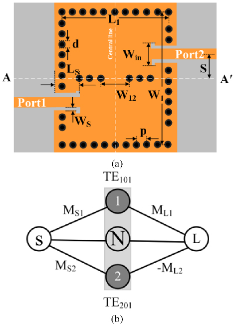
Figure 1: (a) Geometric configuration and (b) topological structure of the dual-mode wide stopband SIW BPF.
The topology of the proposed dual-mode SIW BPF is shown in Fig. 1 (b). Nodes 1 and 2 represent TE and TE modes, respectively. The corresponding coupling matrix is shown in (2). Nodes S and L denote the input and the output ports. The electric field distributions of TE and TE modes are illustrated in Figs. 2 (a) and (b). The TE mode exhibits even symmetry in the electric field distribution, whereas the TE mode exhibits odd symmetry. Increasing the offset distance S enhances the coupling to the TE mode (M) and reduces the coupling to the TE mode (M) because the electric field intensity of the TE mode is the highest at the centerline, and it decays away from the centerline. Oppositely, TE mode shows zero electric field at the centerline, and is increased away from the centerline. When MM, TZs can be introduced outside the passband, with their position determined by the ratio M/M. The ratio can be controlled by the offset distance S. Because M is always greater than M, and f is always less than f, TZs are positioned in the upper stopband. Additionally, node N is a non-resonant node. It is mainly used for bypass coupling created by TE mode and can generate an additional TZ in the upper stopband:
| (2) |
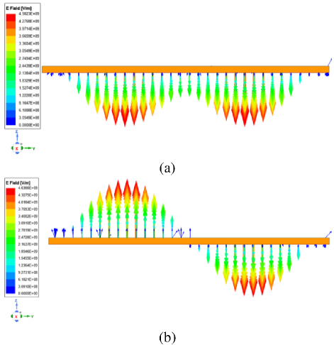
Figure 2: Electric field distributions of (a) TE and (b) TEmodes.
The coupling between the two mode cavities is mainly controlled by the width W. The coupling coefficient can be extracted by the following relation [23]:
| (3) |
where f and f are the high and low resonant frequencies, and k is the coupling coefficient between the dual-mode cavities.
The dual-mode cavity, mainly constructed by the coupling window with width W, can produce magnetic coupling. The coupling coefficient can be extracted with the dual-mode cavity structure shown in Fig. 1 (a). Based on HFSS software, the magnetic coupling coefficient design curve is shown in Fig. 3. It can be seen that the magnetic coupling coefficient is changed with the increment of W. With W in the range of 0-1.5 mm, little change can be seen on the coupling coefficient, indicating weak coupling in this region. When W is larger than 1.5 mm, a significant rise in the coupling coefficient is observed, showing a strong increased coupling effect and a more notable interaction between the dual-mode cavities. Based on the above analysis, W is one of the key parameters for the adjustment of the magnetic coupling effect.
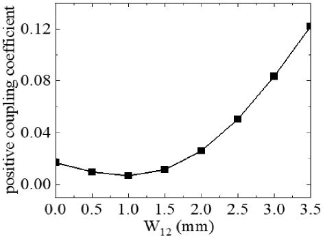
Figure 3: Positive coupling coefficient of coupling structure.
To demonstrate complete control over the positions of TZs, an analysis of the offset distance parameter S is conducted. Figure 4 depicts the transmission characteristics S with various values of S. It can be observed that two TZs are present in the upper stopband, while no TZs are found in the lower stopband. With S increasing, TZ gradually shifts towards higher frequencies with minimal variation, whereas TZ shifts towards lower frequencies with more noticeable changes. As mentioned earlier, the position of the first TZ is mainly determined by the ratio M/M, which can be controlled by modifying the offset S. The smaller the offset S is, the smaller the M/M is, and the closer TZ is to the passband. The location of the second TZ depends primarily on the bypass coupling through the TE mode. As the offset S decreases, the coupling to the TE mode increases, demonstrating that S is a critical parameter for tuning TZ positions and optimizing stopband suppression.
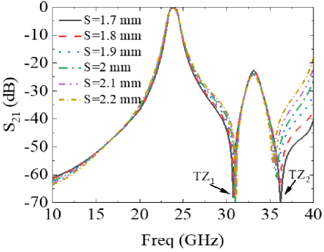
Figure 4: Effects of different S on the TZ positions of the SIW filter.
Figure 5 shows the influences of different L on the stopband of the SIW filter. It is observed that, with fixed W and increased L, the overall frequency response is shifted towards lower frequencies. When L 8 mm, the suppression of f can be reduced to be less than 20 dB, and the coupling of TE and TE modes is weak. At 48.2 GHz, the stopband can be extended to be 2.02f. When L is equal to 7.5 mm or 8.5 mm, the TE and TE modes are coupled to each other, creating a parasitic passband.
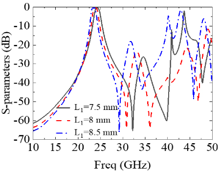
Figure 5: Effects of different L on the stopband of SIW filters.
The perturbed vias are used to further expand the stopband, as illustrated in Fig. 6. These perturbed vias act as metal electric walls, without electric field energy presented. Thus, the electric field distribution of transmission modes within the resonant cavity can be changed. The S-parameters of the second-order SIW BPF based on perturbation via over a wide frequency range and passband range are shown in Fig. 7. The final dimensions are: W 10.16 mm, L 8 mm, W 2.2 mm, S 1.64 mm, L 1.87 mm, W 0.27 mm, W 1.65 mm, Offset 1 mm. In Fig. 7, the center frequency f is 24.1 GHz, with the fractional bandwidth (FBW) of 4.7%, return loss better than 23 dB, and insertion loss below 0.36 dB. At the stopband frequency of 34 GHz, the TE/TE mode achieves suppression depth below 28.8 dB. With out-of-band suppression level below 20 dB, the stopband width reaches 53.5 GHz, corresponding to 2.22f, thereby achieving significant stopband width extension.
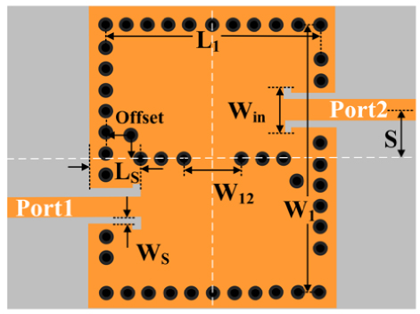
Figure 6: Geometric configuration of second-order wide stopband SIW BPF with perturbed vias.
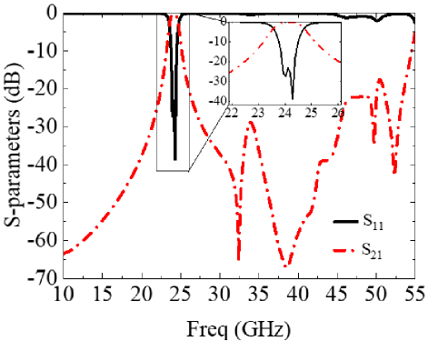
Figure 7: Passband and wideband S-parameters of a second-order SIW BPF with perturbed vias.
III. FOURTH-ORDER SIW BPF
A fourth-order wide stopband SIW BPF is implemented by cascading two similar dual-mode SIW cavities, with the structure shown in Fig. 8 (a). The topology of the proposed fourth-order SIW BPF is shown in Fig. 8 (b). The corresponding coupling matrix is shown in (4). With the designed structure shown in Fig. 8 (a), Port1 and Port2 are symmetrically positioned relative to the centerline (white dashed line) of the vertical vias wall. Internal coupling between the two dual-mode SIW cavities is achieved through a coupling window offset from the vertical centerline of both cavities. Both left and right pairs of cavities are excited simultaneously by TE and TE modes. The coupling strength of TE and TE modes in the two cascaded structures is determined by the width W of the coupling window on the vertical vias wall. The coupling window with a width of W is arranged along the centerline between R2 and R3, which can suppress higher-order resonance modes:
| (4) |
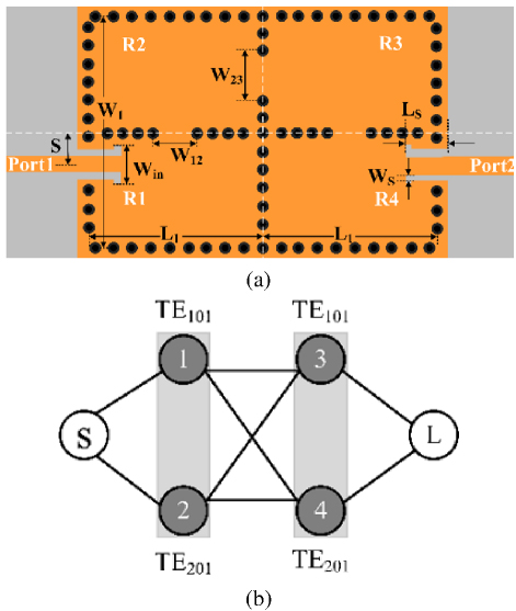
Figure 8: (a) Geometric configuration and (b) topological structure of the fourth-order broadband SIW BPF.
As mentioned earlier, L has an impact on the stopband of SIW filters. Therefore, in order to achieve a wide stopband fourth-order SIW filter, L is designed to be 8 mm. Figure 9 illustrates the passband and wide stopband S-parameters of the fourth-order SIW BPF. The final dimensions are: W 10.16 mm, L 8 mm, W 1.8 mm, W 2.15 mm, S 1.4 mm, L 1.88 mm, W 0.27 mm, W 1.65 mm. As depicted in Fig. 9, within the passband, frequency f is 24.1 GHz, with FBW of 2.32%, return loss better than 26.85 dB, and insertion loss less than 1.26 dB. Within the stopband, the TE/TE modes exhibit attenuation greater than 26.3 dB at 33.4 GHz. With the out-of-band suppression level below 20 dB, the stopband extends to 55.65 GHz, corresponding to 2.31f, demonstrating effective widening of the stopband.
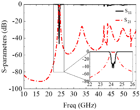
Figure 9: Passband and wide stopband S-parameters of fourth-order SIW BPF.
IV. FOURTH-ORDER CROSS-COUPLED SIW BPF
To enhance the roll-off characteristics and improve frequency selectivity, snake-shaped slots are introduced into the filter design. These slots serve a dual purpose: they modify the coupling between adjacent resonant cavities and generate TZs near the passband edges.
In conventional SIW filters, resonant cavities are coupled positively, allowing signals to propagate in phase. This results in a relatively wide transition band and limits the filter’s ability to meet the stringent selectivity demands of millimeter-wave applications. By contrast, the introduction of snake-shaped slots establishes a negative coupling structure, which alters the signal propagation path and induces phase inversion near the passband. This phase inversion leads to destructive interference with the main transmission path, effectively generating TZs in the frequency response.
The presence of these TZs significantly improves the filter’s performance in two key ways. First, they increase the attenuation rate at the passband edges, effectively sharpening the transition from passband to stopband. This steep roll-off helps suppress unwanted interference from adjacent frequencies, enhancing out-of-band rejection. Second, the reduced transition bandwidth improves frequency selectivity, which is particularly crucial in millimeter-wave applications where spectrumresources are limited and efficient signal isolation is required.
Compared to designs without TZs, the inclusion of snake-shaped slots leads to a substantially steeper roll-off rate and improved frequency selectivity. This makes the filter better suited for applications demanding high spectral purity and minimal adjacent-channel interference.
Based on the fourth-order wide stopband BPF shown in Fig. 8 (a), a snake-shaped coupling slot is etched on the vias wall top layer between SIWs R1 and R4, thereby introducing negative cross-coupling. The serpentine slot design is capable of effectively introducing coupling while ensuring excellent frequency selectivity and low radiation loss without compromising the integrity and shielding effectiveness of the SIW cavity. This characteristic is especially important in high-frequency applications, as high selectivity helps to effectively separate signals from interference, ensuring signal quality and stability. In contrast, other geometries, such as rectangular and circular slots, while widely used in certain cases, often face limitations in achieving TZs, which may result in higher radiation loss or insertion loss. Furthermore, these designs may require more complex manufacturing processes, thereby affecting production efficiency. The geometric configuration and the topology are illustrated in Figs. 10 (a) and (b). Weak coupling is formed between paths 3 and 4, creating a phase difference between the two signal paths and generating a set of TZs.
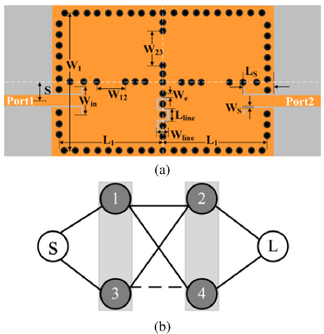
Figure 10: (a) Geometric configuration and (b) topological structure of the fourth-order cross-coupled SIW BPF.
The corresponding coupling matrix is shown in (5). A serpentine slot is loaded between the holes of the SIW cavity connecting the input and output ports to form electrical coupling. HFSS software extracts coupling coefficients based on the serpentine groove structure. The electrical coupling coefficient design curve is shown in Fig. 11. It can be seen that the negative coupling coefficient is decreased with W increasing, indicating that the negative coupling strength is gradually increased. As W is increased from 0.25 mm to 0.65 mm, the negative coupling effect between the two cavities is significantly enhanced, and the coupling strength becomes stronger:
| (5) |
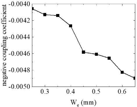
Figure 11: Negative coupling coefficient of coupling structure.
The final dimensions of fourth-order cross-coupled SIW BPF are: W 10.2 mm, L 7.6 mm,W 2.1 mm, W 2.6 mm, S 1.5 mm, L 2.24 mm, W 0.1 mm, W 2.05 mm, W 0.35 mm, W 0.85 mm, L 0.9 mm. The structure diagram of the prototype fourth-order cross-coupled SIW BPF is shown in Fig. 12. Figure 13 illustrates simulated and measured responses. The measured results are in good agreement with the simulation results. The simulated center frequency f is 24.1 GHz with a minimum insertion loss of 0.75 dB and return loss better than 20.18 dB. Two TZs are observed at 22.7 GHz and 25.14 GHz, with suppressions of 54.65 dB and 37.95 dB, respectively. The measured center frequency f is 24.1 GHz with a minimum insertion loss of 0.52 dB and return loss better than 11.8 dB, revealing TZs at 22.82 GHz and 25.15 GHz with suppression levels below 20 dB.
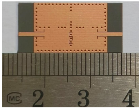
Figure 12: Photograph of the fourth-order cross-coupled SIW BPF.
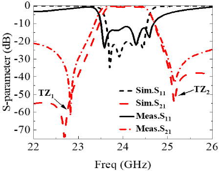
Figure 13: S-parameters of the fourth-order cross-coupled SIW BPF.
The out-of-band suppression is better than 40 dB in the simulation and better than 20 dB in the actual measurement. Although the measured out-of-band suppression is lower than the simulated result, the TZ in the lower stopband is closer to the passband, showing better frequency selectivity than the simulation. The insertion loss is further decreased after loading the coupling slot. The difference of the return loss between the simulation and the measurement in Fig. 13 can be attributed to manufacturing errors, soldering of SMA connectors, and parasitic effects from test fixtures, connectors, and measurement equipment. These factors can introduce additional losses and reflections, which reduce the out-of-band suppression effectiveness. During the simulation process, certain physical phenomena may not have been fully included, such as the parasitic effects at high frequencies and the non-ideal characteristics of the substrate materials. Additionally, the materials used in actual measurements may differ from the simulations, such as variations in dielectric constant and loss factor. The testing environment may also impact the results. Changes in temperature and humidity, as well as the calibration status of the measurement equipment, may lead to errors in the results. Furthermore, the connection methods and layout design of the test fixtures may also affect signal transmission and measurement to some extent:
| (6) |
According to (6), when f is 24.1 GHz, the bandwidth is 1.133 GHz, Q is 21.26, and Q is 452.
After TZs through serpentine slots to optimize the roll-off characteristics at the passband edges, attention should still be given to the suppression of higher-order frequencies. Although TZs effectively mitigate interference near the passband, their influence is primarily concentrated at specific frequency points, with limited impact on higher-order resonant frequencies. In millimeter-wave SIW filters, these higher-order resonant frequencies can introduce unwanted interference outside the passband, which may degrade overall system performance, particularly in spectrally dense environments. Therefore, the suppression of higher-order frequencies is regarded as an important step in enhancing the overall performance of the filter.
To more effectively attenuate higher-order frequencies, the design of the serpentine slots can be optimized. Specifically, as shown in Fig. 14, reducing the diameter of the metal vias above and below the serpentine slots, and increasing the distance between the vias and the slots, can significantly reduce the coupling effect of the serpentine slots on higher-order modes. This design adjustment effectively mitigates the excitation of higher-order modes, further optimizing the filter’s high-frequency attenuation characteristics.
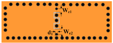
Figure 14: Optimization design of the serpentine slot section.
The diameter and positioning of the metal vias around the serpentine slots are shown in Fig. 15, which presents four distinct configurations. The first configuration represents the initial case, where the via diameter is d d 0.4 mm, and the vias are positioned at the standard distance from the serpentine slot, with W W 0.35 mm. The second configuration reduces the via diameter to d 0.3 mm, while maintaining W W 0.35 mm. The third configuration increases the distance between the vias and the serpentine slot, with W 0.53 mm, W 0.84 mm, and the via diameter remaining at d 0.4 mm. The final configuration combines both optimizations, where the vias are moved further away from the serpentine slot (W 0.53 mm, W 0.84 mm), and the via diameter is reduced to d 0.3 mm.
By comparing these four configurations, it can be observed that both reducing the via diameter and increasing the distance between the vias and the serpentine slot effectively mitigate the impact of higher-order modes. Specifically, reducing the via diameter helps weaken the coupling between higher-order modes, while distancing the vias from the serpentine slot reduces unnecessary interference signals. When these two optimization strategies are combined, they significantly suppress the influence of higher-order frequencies, enhancing the filter’s ability to reject interference and out-of-band signals at higher frequencies, thereby improving the overall performance of the filter.
However, it is important to note that this optimization leads to a decrease in the filter’s selectivity. In other words, although the suppression of higher-order frequencies is enhanced, the corresponding selectivity worsens. This trade-off is an inevitable consequence of the attenuation process of higher-order frequencies.
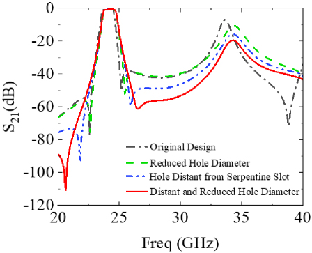
Figure 15: Effect of via hole diameter and position on serpentine slot performance.
Table 1: Comparison of this design with other types of filters
| Ref. | f(GHz) | FBW(%) | Size() | IL(dB) | NP | NZ | Layers | Size(mm) |
| [24] | 20.5 | 4 | 1.93 | 0.9 | 4 | 2 | 1 | 1413.43 |
| [25] | 5 | 2.9 | 1.30 | 6.35 | 4 | 2 | 1 | 35.935.7 |
| [26] | 7.5 | 5.2 | 1.15 | 1.5 | 3 | 2 | 1 | 52.416 |
| [27] | 10 | 3.3 | 2.97 | 1.55 | 4 | 2 | 1 | 39.430.9 |
| [28] | 9.95 | 3.1 | 2.09 | 2.1 | 4 | 2 | 1 | 3028.81 |
| [29] | 26.8 | 7 | 1.74 | 2.1 | 4 | 4 | 2 | 10.98.52 |
| [30] | 5.45 | 11.2 | 1.73 | 4 | 2 | 0 | 1 | 96.549.4 |
| This work | 24.1 | 4.7 | 2.20 | 0.52 | 4 | 2 | 1 | 15.210.2 |
f: center frequency; FBW: fractional bandwidth; IL: insertion loss; NP: number of poles; NZ: number of TZs.
Figure 16 shows the passband and wide stopband S-parameters of a fourth-order SIW BPF with suppressed higher-order modes. The final dimensions are: W 10.16 mm, L 7.5 mm, W 2.19 mm, W 2.61 mm, S 1.99 mm, L 2.27 mm, W 0.1 mm, W 1.69 mm, W 0.53 mm, W 0.84 mm, d 0.3 mm, W 1 mm, L 0.9 mm. As shown in Fig. 16, within the passband, the frequency f is 24.1 GHz, with FBW of 4.5%, return loss better than 20 dB, and insertion loss less than 0.7 dB. In the stopband, the attenuation of TE/TE modes exceeds 20 dB at 34.2 GHz. The stopband extends to 40 GHz (1.66f) when the out-of-band suppression level is below 20 dB, indicating an effective widening of the stopband.
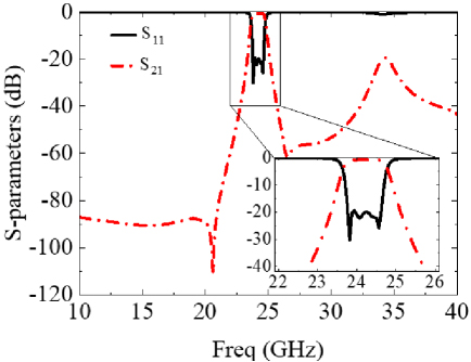
Figure 16: The passband and wide stopband S-parameters of high-order suppressed fourth-order SIW BPF.
Table 2: Comparison of this design with other cross-coupled structures
| Ref. | f(GHz) | FBW(%) | Size() | IL(dB) | NP | NZ | Layers | Size(mm) |
| [31] | 2.2 | 5.5 | 0.47 | 1.55 | 4 | 2 | 4 | 49.246 |
| [32] | 26.1 | 10.5 | 8.91 | 2.65 | 6 | 2 | 1 | 2221 |
| [33] | 12.5 | 9 | 7.07 | 1.3 | 6 | 2 | 1 | 23.517.5 |
| [34] | 5.75 | 2 | 2.12 | 2.2 | 4 | 2 | 1 | 3635.7 |
| [35] | 4.5 | 3.7 | 0.51 | 2.1 | 4 | 3 | 2 | 2525 |
| [36] | 38.8 | 5.9 | 4.38 | 6.7 | 6 | 2 | 2 | 13.15.75 |
| This work | 24.1 | 4.7 | 2.20 | 0.52 | 4 | 2 | 1 | 15.210.2 |
f: center frequency; FBW: fractional bandwidth; IL: insertion loss; NP: number of poles; NZ: number of TZs.
Comparison between the proposed fourth-order cross-coupled SIW BPF and the published results is listed in Table 1. It can be seen that the design in this paper shows more compact size and lower insertion loss (IL). A filter with narrower bandwidth can provide better frequency selectivity, allowing the filter to effectively distinguish the target signal from interference. This is particularly important in signal processing, especially in high-frequency communication systems such as millimeter-wave communication and radar applications, which typically have high demands for frequency selectivity and insertion loss. Additionally, a moderate bandwidth design is beneficial in reducing insertion loss, ensuring effective signal transmission and overall system performance. Therefore, although modern communication systems generally pursue wider bandwidths, a careful balance between the signal quality and the transmission stability is considered in our design at specific frequencies.
It is noteworthy that the size of the design in [23] is smaller than our design. However, its insertion loss is 0.9 dB, with narrower bandwidth. In [24–27], those designs are limited to lower frequency bands with higher ILs. Additionally, the miniaturization achieved in [28] is due to a complex multilayer structure, whereas the planar layout in the paper is simpler. The inflatable SIW filter used in [29] can achieve a wide bandwidth but it has a very high insertion loss of 4 dB and does not include TZs. Additionally, the manufacturing process for inflatable SIW filters is often complex, requiring strict control over materials and structures, which may lead to higher production costs. Furthermore, the stability of inflatable SIW filters during long-term use also needs to be considered, particularly in high-frequency applications where even minor structural changes can affect the performance. In contrast, the design proposed in this paper, based on a single-layer PCB structure, is easy to fabricate, allowing for the realization of a high-performance filter with low cost. Moreover, the stability of this design in high-frequency signal transmission is effectively ensured.
V. DISCUSSION
In SIW filter design, electrical coupling is achieved by using metal surface slits, which is a common and effective technique. The surface current of the TE mode is significantly suppressed by the open slot-line structures. As a result, radiation losses are introduced, with reduced shielding effectiveness and degraded quality factors.
Table 2 shows the comparison between the fourth-order cross-coupled SIW BPF proposed in this paper and other reported cross-coupled designs. Significant advantages are shown by the filter design in this paper, and it is seen to be more competitive compared to the designs in other literature. Serpentine slots are introduced on copper pillar walls, which do not cause large radiation losses. An insertion loss of only 0.52 dB is achieved, which is much lower than the 2.65 dB reported in [31] and the 2.2 dB in [34], indicating excellent signal transmission efficiency. Although the physical size is 15.210.2 mm, a wavelength area of 2.20 is reached. This is more compact and of greater efficiency compared to other designs with larger size, e.g. 8.91 in [31] and 7.07 in [32]. Additionally, a single-layer structure is used in this paper, which greatly simplifies the manufacturing process. Compared to the four-layer structure used in [30], both the complexity and the cost are reduced, and easier integration into various systems is achieved. The filter in this paper shows advantage over the design in [33]. Both the designs in this paper and in [33] show similar structure, except a low-frequency band with a narrower bandwidth is applied in [33].
Specifically, two significant transmission zeros (TZ and TZ) are successfully introduced in the filter design of this paper, located near 22.5 GHz and 25 GHz. These TZs greatly improve the filter’s frequency selectivity. At the TZ locations, a suppression depth of over 60 dB is achieved, which is much better than that of the multi-layer cross-coupled design shown in [35]. Although some out-of-band suppression capability is shown by the multi-layer cross-coupled filters, no clear TZs are exhibited. No TZs are seen in the lower stopband, and the upper stopband has a TZ that is not very noticeable. The simulation results of the filter in this paper coincide with the measured data closely across the entire frequency range, especially near the TZs, indicating high consistency and reliability in design and manufacturing. In contrast, while basic agreement between measurements and simulations is shown by the multi-layer filters, noticeable deviations are found in certain frequency ranges (such as around 37 GHz), particularly in out-of-band suppression.
Additionally, better performance in insertion loss is shown by the filter in this paper, which maintains low insertion loss and improves overall signal transmission quality. In contrast, higher insertion loss is found in the multi-layer filter design, and out-of-band suppression has room for improvement. Thus, clear advantages in frequency selectivity, suppression performance, and consistency are demonstrated by the filter design in this paper, making it more suitable for high-demand communication systems.
VI. CONCLUSION
In this paper, a novel fourth-order bandpass filter based on a cross-coupled structure is proposed. The filter shows a pair of TZs, thereby enhancing frequency selectivity. The resonant characteristics of the first six resonant modes in the proposed single-multi-mode SIW cavity is studied, validating the feasibility of a bandpass filter in terms of frequency and bandwidth control. Based on this exploration, three SIW filters are designed and studied, demonstrating the wide stopband characteristics of the second-order and the fourth-order SIW bandpass filters. Furthermore, a fourth-order SIW filter with a pair of TZs is designed, fabricated, and measured, showing good agreement between the simulated and the measured results. This technology stands as a competitive candidate for developing high-performance SIW filters in microwave/radio circuit and system applications, particularly suitable for high-frequency wireless communication systems such as 5G and IoT applications.
ACKNOWLEDGMENT
This research was funded by the Fujian Natural Science Foundation Project grant number 2022J01823 and Technology Subsidy Project (2024CXY0314).
REFERENCES
[1] P. Li, H. Chu, and R.-S. Chen, “Design of compact bandpass filters using quarter-mode and eighth-mode SIW cavities,” IEEE Trans. Compon. Packag. Manuf. Technol., vol. 7, no. 6, pp. 956-963, June 2017.
[2] Z. Liu, G. Xiao, and L. Zhu, “Triple-mode bandpass filters on CSRR-loaded substrate integrated waveguide cavities,” IEEE Trans. Compon. Packag. Manuf. Technol., vol. 6, no. 7, pp. 1099-1105, July 2016.
[3] X. Zhou, G. Zhang, S. Feng, K. W. Tam, Z. Zhang, and W. Tang, “Design of 3-D integrated SIW multiband bandpass filter with split-type extended doublet topology,” IEEE Trans. Compon. Packag. Manuf. Technol., vol. 12, no. 10, pp. 1681-1691, Oct. 2022.
[4] X.-P. Chen and K. Wu, “Substrate integrated waveguide filter: Basic design rules and fundamental structure features,” IEEE Microw. Mag., vol. 15, no. 5, pp. 108-116, July/Aug. 2014.
[5] Y. Zheng, Y. Zhu, Z. Wang, and Y. Dong, “Compact, wide stopband, shielded hybrid filter based on quarter-mode substrate integrated waveguide and microstrip line resonators,” IEEE Microw. Wireless Compon. Lett., vol. 31, no. 3, pp. 245-248, Mar. 2021.
[6] P. Chu, L. Guo, L. Zhang, F. Xu, W. Hong, and K. Wu, “Wide stopband substrate integrated waveguide filter implemented by orthogonal ports’ offset,” IEEE Trans. Microw. Theory Techn., vol. 68, no. 3, pp. 964-970, Mar. 2020.
[7] G. Lin and Y. Dong, “A compact, hybrid SIW filter with controllable transmission zeros and high selectivity,” IEEE Trans. Circuits Syst. II Exp. Briefs, vol. 69, no. 4, pp. 2051-2055, Apr. 2022.
[8] Y. Zhu and Y. Dong, “A compact dual-band quasi-elliptic filter based on hybrid SIW and microstrip technologies,” IEEE Trans. Circuits Syst. II Exp. Briefs, vol. 69, no. 3, pp. 719-723, Mar. 2022.
[9] W. Shen, “Extended-doublet half-mode substrate integrated waveguide bandpass filter with wide stopband,” IEEE Microw. Wireless Compon. Lett., vol. 28, no. 4, pp. 305-307, Apr. 2018.
[10] Y. Zhu and Y. Dong, “A compact dual-band quasi-elliptic filter based on hybrid SIW and microstrip technologies,” IEEE Trans. Circuits Syst. II Exp. Briefs, vol. 69, no. 3, pp. 719-723, Mar. 2022.
[11] G. Lin and Y. Dong, “A compact, hybrid SIW filter with controllable transmission zeros and high selectivity,” IEEE Trans. Circuits Syst. II Exp. Briefs, vol. 69, no. 4, pp. 2051-2055, Apr. 2022.
[12] L. Gu and Y. Dong, “Compact half-mode SIW filter with high selectivity and improved stopband performance,” IEEE Microw. Wireless Compon. Lett., vol. 32, no. 9, pp. 1039-1042, Sep. 2022.
[13] M. R. Jiao, F. Zhu, P. Chu, W. Yu, and G. Q. Luo, “Compact hybrid bandpass filters using substrate-integrated waveguide and stripline resonators,” IEEE Trans. Microw. Theory Techn., vol. 72, no. 1, pp. 391-400, Jan. 2024.
[14] Y.-X. Yan, W. Yu, and J.-X. Chen, “Millimeter-wave low side- and back-lobe SIW filtenna array fed by novel filtering power divider using hybrid TE/TE mode SIW cavities,” IEEE Access, vol. 9, pp. 167706-167714, Dec. 2021.
[15] G. Lin, Y. Dong, and X. Luo, “Miniaturized quarter-mode SIW filters loaded by dual-mode microstrip resonator with high selectivity and flexible response,” IEEE Microw. Wireless Compon. Lett., vol. 32, no. 6, pp. 660-663, June 2022.
[16] Z. Chen, M. Wang, D. Guan, Z. Qian, W. Wu, and L. Zhu, “Wideband filtering antenna fed through hybrid substrate integrated waveguide and spoof localized surface plasmon structure,” IEEE Trans. Antennas Propa., vol. 70, no. 5, pp. 3812-3817, May 2022.
[17] D. Li, W. Luo, X. Chen, Y. Liu, K.-D. Xu, and Q. Chen, “Miniaturized dual-/tri-/quad-band bandpass filters using perturbed multimode SIW cavity,” IEEE Trans. Compon. Packag. Manuf. Technol., vol. 13, no. 10, pp. 1685-1693, Oct. 2023.
[18] M.-H. Ho and K.-H. Tang, “Miniaturized SIW cavity tri-band filter design,” IEEE Microw. Wireless Compon. Lett., vol. 30, no. 6, pp. 589-592, June 2020.
[19] H.-W. Xie, K. Zhou, C.-X. Zhou, and W. Wu, “Substrate-integrated waveguide triple-band bandpass filters using triple-mode cavities,” IEEE Trans. Microw. Theory Techn., vol. 66, no. 6, pp. 2967-2977, June 2018.
[20] P. Liu, Z. Li, M. Qin, J. Yin, and X. Qiu, “Two compact bandpass filters with controllable band based on eighth-mode substrate integrated waveguide,” IEEE Trans. Circuits Syst. II Exp. Briefs, vol. 71, no. 2, pp. 932-936, Feb. 2024.
[21] Q. Liu and L. Zhu, “Design of cross-coupled bandpass filters with flexible coupling via half-mode substrate-integrated waveguide,” Int. J. RF Microw. Comput.-Aided Eng., vol. 2024, pp. 1-13, 2024.
[22] P. Chu, M. Luo, J. Zhou, L. Guo, F. Zhu, and L. Zhang, “Dual-band substrate integrated waveguide filter with independent TE and TEcoupling,” IEEE Trans. Microw. Theory Techn., vol. 72, no. 3, pp. 1877-1885, Mar. 2024.
[23] J.-S. Hong and M. J. Lancaster, Microstrip Filter for RF/Microwave Applications. New York: Wiley, 2001.
[24] X.-P. Chen and K. Wu, “Substrate integrated waveguide cross-coupled filter with negative coupling structure,” IEEE Trans. Microw. Theory Techn., vol. 56, no. 1, pp. 142-149, Jan. 2008.
[25] C. J. You, Z. N. Chen, X. W. Zhu, and K. Gong, “Single-layered SIW post-loaded electric coupling-enhanced structure and its filter applications,” IEEE Trans. Microw. Theory Techn., vol. 61, no. 1, pp. 125-130, Jan. 2013.
[26] P. Chu, P. Zhu, J. Feng, L. Guo, L. Zhang, and F. Zhu, “Substrate integrated waveguide filter with flexible mixed coupling,” IEEE Trans. Microw. Theory Techn., vol. 71, no. 9, pp. 4003-4011, Sep. 2023.
[27] F. Zhu, G. Q. Luo, B. You, X. H. Zhang, and K. Wu, “Planar dual-mode bandpass filters using perturbed substrate-integrated waveguide rectangular cavities,” IEEE Trans. Microw. Theory Techn., vol. 69, no. 6, pp. 3048-3057, June 2021.
[28] A. R. Azad and A. Mohan, “Substrate integrated waveguide cross-coupled bandpass filter with wide-stopband,” in 2020 URSI Regional Conference on Radio Science (URSI-RCRS), Varanasi, India, pp. 1-4, 2020.
[29] K. Gong, W. Hong, Y. Zhang, P. Chen, and C. J. You, “Substrate integrated waveguide quasi-elliptic filters with controllable electric and magnetic mixed coupling,” IEEE Trans. Microw. Theory Techn., vol. 60, no. 10, pp. 3071-3078, Oct. 2012.
[30] A. Moznebi, K. Afrooz, and M. Danaeian, “High-performance filtering power divider based on air-filled substrate integrated waveguide technology,” ETRI J., vol. 45, no. 2, pp. 338-345, July 2022.
[31] A. A. Khan, A. Gupta, and M. K. Mandal, “Multilayer cross-coupled SIW filter with next harmonic suppression,” in 2022 IEEE Microwaves, Antennas, and Propagation Conference (MAPCON), Bangalore, India, pp. 68-73, 2022.
[32] X. Zhang, Y. Ji, W. Chen, J. Zhou, and M. Wang, “Design of a high outband rejection cross-coupled SIW filter for millimeter wave communications,” in 2019 International Conference on Microwave and Millimeter Wave Technology (ICMMT), Guangzhou, China, pp. 1-3, 2019.
[33] D. L. Diedhiou, E. Rius, J.-F. Favennec, and A. El Mostrah, “Ku-band cross-coupled ceramic SIW filter using a novel electric cross-coupling,” IEEE Microw. Wireless Compon. Lett., vol. 25, no. 2, pp. 109-111, Feb. 2015.
[34] S. Sirci, M. Á. Sánchez-Soriano, J. D. Martı´nez, V. E. Boria, F. Gentili, W. Bösch, and R. Sorrentino, “Design and multiphysics analysis of direct and cross-coupled SIW combline filters using electric and magnetic couplings,” IEEE Trans. Microw. Theory Techn., vol. 63, no. 12, pp. 4341-4354, Dec. 2015.
[35] B. Lee, G. Lee, and J. Lee, “Two-layered cross-coupled post-loaded SIW filter with microstrip ports,” IEEE Trans. Circuits Syst. II Exp. Briefs, vol. 70, no. 4, pp. 1346-1350, Apr. 2023.
[36] G. Lee, B. Lee, J.-Y. Jeong, and J. Lee, “Ka-band surface-mount cross-coupled SIW filter with multi-layered microstrip-to-GCPW transition,” IEEE Access, vol. 7, pp. 66453-66462, 2019.
BIOGRAPHIES

Yawen He was born in Nanjing, China, in 2001. She received the bachelor’s degree in communication engineering from Wuyi University, Nanping, China, in 2023. She is currently working toward the Postgraduate degree in Information and Communication Engineering, Jimei University, Xiamen, China. Her research interest is RF microwave millimeter wave circuit design.

Zhonghua Ma was born in Gansu, China, in 1973. He received his Ph.D. in Microelectronics from Lanzhou University, Lanzhou, China, in 2018. His present research interests include antenna techniques, RF and microwave circuits design and IoT.

Mengnan Wangwas born in Pingdingshan, China, in 2000. She received the bachelor’s degree in communication engineering from Zhengzhou University of Aeronautics, Zhengzhou, China, in 2022. She is currently working toward the Postgraduate degree in Information and Communication Engineering, Jimei University, Xiamen, China. Her research interest is chipless RFID sensors.

Jingyao Huang was born in Xiamen, China, in 2004. She is currently pursuing her B.S. degree with the Department of Communication Engineering, Jimei University, Xiamen, China. Her research interests are in microwave technology and rectenna technology.

Yanfeng Jiang was born in Jilin, China, in 1972. He received the B.S. degree in Electrical Engineering from Southeast University, Nanjing, China, in 1993, and Ph.D. degree in Microelectronics from Lanzhou University, Lanzhou, China, in 2000. He is now full professor in Jiangnan University, Wuxi, China. His research interests include integrated circuit design, power semiconductor devices and magnetic devices.
ACES JOURNAL, Vol. 40, No. 4, 350–362
doi: 10.13052/2024.ACES.J.400409
© 2025 River Publishers