A Novel Matching Technique for Microstrip Feeds usingOptimized Tapering
Nasim Zahra, Inam Elahi Rana, Farooq Mukhtar, and Mahrukh Khan
1Department of Electrical Engineering
University of Engineering and Technology, Lahore, 54890, Pakistan
nasimzahra132@hotmail.com, mukhtar.farooq@uet.edu.pk
2Department of Electrical, Electronics and Computer Systems
University of Sargodha, 40162, Pakistan
nasim.zahra@uos.edu.pk
3Bismillah Electronics
Lahore, 54600, Pakistan
ierana@biselectronics.net
4Electrical and Computer Engineering Department, The College of New Jersey
Ewing, NJ 08628, USA
khanm@tcnj.edu
Submitted On: December 26, 2024; Accepted On: April 23, 2025
ABSTRACT
This paper presents an efficient impedance matching technique for microstrip feed structures, providing a practical solution for seamless connector integration in high-frequency systems. Unlike conventional approaches that assume predefined connector compatibility, this method allows adaptation to various connector constraints without requiring major structural modifications. A linearly tapered microstrip feed with tapered substrate is proposed to ensure stable impedance matching, reduce signal reflection, and enhance overall system performance. The technique is demonstrated on a fabricated substrate-integrated waveguide antenna, utilizing a Rogers RT/Duroid 5880 substrate configured for 50 impedance and adapted for integration with a specific coaxial connector. Experimental validation confirms excellent agreement between simulated and measured results, verifying its effectiveness in achieving impedance matching, minimizing return loss, and ensuring seamless integration with the connector while preserving radiation characteristics. This work presents a versatile feed design approach that addresses a key challenge in RF and microwave engineering, paving the way for improved performance and broader applicability in advanced communication systems and integrated circuit applications.
Index Terms: 5G antenna, impedance matching technique, microstrip feed, microstrip transition, substrate-integrated waveguide, tapered microstrip.
I. INTRODUCTION
The increasing demand for high-performance microwave and RF systems has driven extensive research into impedance-matching techniques for microstrip feed structures. Efficient impedance matching is critical for ensuring minimal signal reflection and optimal power transfer, particularly in high-frequency applications. A key challenge arises when microstrip feeds must interface with standard coaxial connectors, such as SMA connectors, whose dimensional constraints often lead to impedance mismatches with conventional microstrip feeds, thereby degrading overall system performance. At high frequencies, the coaxial connector pin becomes too thin for effective connection to the structure due to its small diameter, which prevents the wave from being launched efficiently.
Table 1: Comparison of transition techniques
| Parameter | Waveguide-Based [1–9] | Direct Coaxial [10–11] | Proposed Work |
| Bandwidth | Narrowband (cutoff-limited) | Wideband (connector-limited) | Wideband (connector-limited) |
| Adaptability | Fixed dimensions (e.g., WR-90) | Connector specific | Connector-adaptable |
| Extra components for Impedance Matching | Stepped ridges [9, 12] & impedance transformers [13] | Simple or Radial stubs [14] | None |
| Fabrication | Complex – requires precise alignment, mode converters, & adapters | Low to Moderate – might involve simple or radial stub etching | Simple |
| Scalability | Suited to standards (e.g., X-band) | challenges for miniaturization | scalable for next gen. systems |
| Sensitivity to manufacturing tolerances | High | Low | Low |
| Connector Compatibility | Low – Need for specialized interfaces | Good – integrates with predefined connectors | High – adaptive for integration with available connectors. |
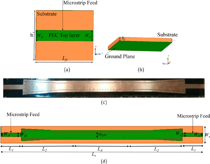
Figure 1: Conventional simple tapered microstrip feed design to planar rectangular waveguide or SIW: (a) Top view, (b) Oblique View, (c) Fabricated feed integrated with SIW antenna [17], and (d) Feed part indicated by on both ends of the antenna [17].
Existing approaches to microstrip-to-coaxial transitions have primarily focused on either waveguide-based transformations or direct microstrip-to-coaxial transitions. Waveguide-based transitions [1–9] offer high performance but may require additional components, leading to increased bulk, sensitivity to manufacturing variations, precise alignment requirements, and added fabrication complexity. Since most electronic systems are equipped with coaxial ports, they are generally preferred over waveguide ports to simplify integration, making a direct microstrip-compatible transition more desirable. However, direct microstrip-to-coaxial transitions [10–11] typically assume predefined connector compatibility, restricting their adaptability to varying design constraints. Moreover, techniques using stepped ridges [9, 12], impedance transformers [13], and radial stubs [14] improve impedance matching but do not specifically address the integration challenges imposed by connector dimensional limitations. Also, fixed connector-specific designs require structural redesign for evolving miniaturized standards (5G/6G), highlighting scalability challenges. This gap motivates the development of a compact, adaptable, and fabrication-friendly impedance-matching technique for microstrip feeds that ensures seamless microstrip-to-coaxial integration without requiring significant structural modifications.
In response, this work introduces a novel impedance-matching technique based on an optimized linearly tapered microstrip transition with tapered substrate. This approach minimizes signal reflection and preserves signal integrity while adapting the feed to the physical constraints imposed by available connectors. The method offers a direct and efficient solution, ensuring wideband performance without adding fabrication complexity. The primary contributions of this study include the development of the optimized tapered transition and the elimination of additional matching components. Experimental validation confirms strong agreement between simulated and measured results. Table 1 presents a comparative summary of different transition techniques.
The remainder of this paper is organized as follows. Section II presents the design methodology and theoretical formulation, detailing the development of the optimized transition. Section III discusses simulation and experimental results that confirm the efficacy of the proposed approach. Finally, section IV concludes the paper with a summary of key findings and futuredirection.
II. PROPOSED MICROSTRIP FEED DESIGN
In this work, a microstrip feed is designed for integration with a substrate-integrated waveguide (SIW) antenna fabricated on the same substrate. Among various SIW feed structures [15], the microstrip feed is selected for its extensive use in planar circuit designs and its ability to offer broad bandwidth coverage across the entire SIW spectrum. Design equations from [16] are employed to calculate the microstrip width (w) based on a given substrate height (h) and the targeted port impedance. The conventional microstrip feed, as described in [10], is carefully configured to match the port impedance with its characteristic impedance (), thereby ensuring optimal power transfer and minimal signal reflection, using the formulations presented in [11]. Specifically, equations from [16] indicate that the microstrip trace width at the port interface should be for a Rogers RT/Duroid 5880 substrate of height and a target impedance of 50 . Furthermore, the optimum taper length and corresponding terminal width for the transition to the SIW are computed to be and , respectively, using the formulas from [11]. Figure 1 illustrates the fabricated conventional microstrip feed design integrated with the SIW antenna.
However, the conventional microstrip feed dimensions, and , are incompatible with the available 50 SMA840A-0000 connector. To ensure connector compatibility while preserving a 50 port impedance, the substrate thickness should be reduced to 20 mils (denoted as ), and the corresponding microstrip width is recalculated as using the formula in [16]. It is essential that the transition to instead of and from to occurs gradually rather than abruptly. In pursuit of this, the subsequent formulas and procedures are applied to optimize the tapered length.
A. Secondary taper for microstrip feed
The objective is to design a secondary taper for an already fabricated microstrip feed, which originally tapers from to in width and with a constant substrate height of . The goal is to achieve SMA connector compatibility by applying another taper to reduce the substrate height to and microstrip width to gradually, ensuring that the impedance is matched and is minimized below -10 dB.
Table 2: Key design parameters and dimensions
| Parameter | Symbol | Value (mm) | Parameter | Symbol | Value (mm) |
| Substrate Integrated Waveguide Antenna | |||||
| Microstrip to SIW transition | 28.22 | SIW to antenna section transition | 74 | ||
| Radiating Section (antenna length) | 75 | Substrate Thickness | 1.575 | ||
| Substrate Length | 279.44 | Substrate Width | 23 | ||
| Ground Plane Length | Ground Plane Width | ||||
| SIW width in radiating section | 8.32 | ||||
| Simple Tapered Microstrip Feed | |||||
| Feed section Length | Tapered Section Length | ||||
| Tapered Width (initial) | 4.9 | Tapered Width (final) | 5 | ||
| Tapered section substrate height | |||||
| Proposed Tapered Microstrip Feed | |||||
| Feed section Length | Secondary Tapered Section Length | 10.4 (optimal) | |||
| Secondary Tapered section Width (initial) | 1.578 | Secondary Tapered section Width (final) | 4.932 (optimal) | ||
| Secondary Tapered section substrate height (initial) | 0.508 | Secondary Tapered section substrate height (final) | |||
Width at :
Substrate height at :
Width at :
Substrate height at :
Length of taper : Unknown but constrained by
Microstrip Impedance Formula: The characteristic impedance for a microstrip line, based on the variable width and substrate height , is approximated from [16] as follows:
(1) Linear Taper Functions: The microstrip width and substrate height taper linearly from to as follows:
(2) where .
(3) Reflection Coefficient : is based on the mismatch between along the taper and the 50 SMA connector:
(4)
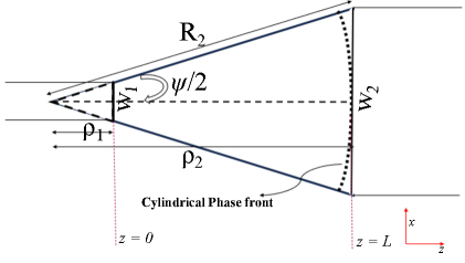
Figure 2: Top view of E-plane horn-like configuration for proposed tapered microstrip feed.
B. Optimization problem
So the optimization problem can be expressed as:
| (5) |
Subject to:
| (6) |
| (7) |
| (8) |
| (9) |
where, . is free space wavelength and is the relative permittivity of dielectric.
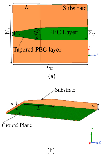
Figure 3: Proposed tapered microstrip feed design for a planar rectangular waveguide or SIW: (a) Top view and (b) Oblique View.
Constraint (9) is derived to minimize the phase error associated with the cylindrical phase front of the wave launched into the waveguide as the proposed feed resembles an E-plane horn. Referring to Fig. 2, the derivation of (9) is provided in appendix A.
C. Optimization procedure
Initial Guess: Start with an initial estimate for and , ensuring .
Iterative Optimization:
Calculate along the taper.
Compute from impedance mismatch.
Adjust and iteratively to minimize .
Convergence Criteria: Stop when stays below -10 dB across the taper, ensuring impedance matching.
This optimization problem can be solved using numerical methods or simulation tools to find the optimal taper length L that minimizes the impedance mismatch across the taper. The length for this gradual change is determined through optimization conducted in HFSS software, fine-tuning the design for its intended performance, and is found to be 10.4 mm. Figure 3 illustrates the proposed microstrip design along with all dimensions for the SIW antenna fabricated in [17]. Table 2 presents the key design parameters and dimensions across different structures.
III. IMPLEMENTATION AND RESULTS
The proposed microstrip feed is implemented using a cost-effective approach with minimal modifications. The process begins with the selective removal of the copper cladding on the top layer up to a length . This is followed by carefully reducing the substrate height through mechanical polishing to create a tapered profile over the same length. To restore conductivity in the modified area and ensure continuous signal transmission, readily available materials such as copper strips, foils, or adhesive copper tape are applied. Figure 4 shows the proposed feed design integrated with the SIW antenna, demonstrating its successful implementation and connection to a standard SMA connector, specifically the SMA840A, which is well-suited for high-frequency applications up to 26.5 GHz. It should be noted that the signal pin of the connector is not in contact with the tapered section of the substrate at a single point; instead, it is properly soldered beneath the entire length of the pin.
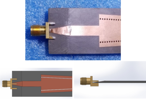
Figure 4: Visualization of the proposed microstrip feed design for SIW leaky wave antenna fabricated in [17].
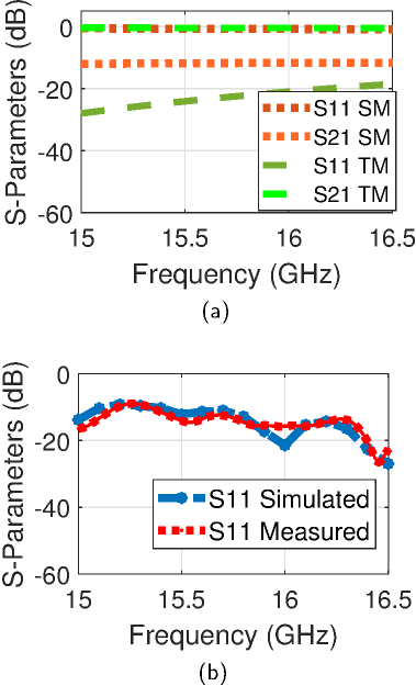
Figure 5: S-parameters of: (a) simple and the proposed tapered microstrip feed designs (SM and TM) simulated as independent feed structures and (b) the SIW leaky-wave antenna integrated with the proposed feed design (TM).
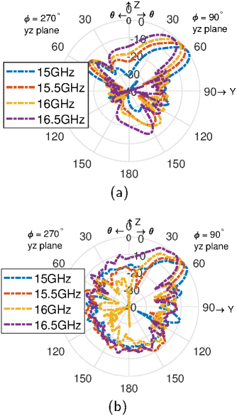
Figure 6: Radiation patterns in the elevation plane for the SIW leaky-wave antenna demonstrating radiation perseverance: (a) Expected and (b) Measured.
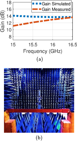
Figure 7: (a) Simulated and measured gain results and (b) Measurement setup in anechoic chamber.
The two different feed structures shown in Figs. 1 and 3 are individually simulated using HFSS software, incorporating connector model of specific dimensions. However, when evaluating connector compatibility, it becomes evident that the proposed tapered feed aligns well with the SMA840A connector utilizing a substrate height of 20 mils () at the port end. In contrast, the simple tapered microstrip feed employs a substrate height of . Figure 5 (a) illustrates that the simple tapered microstrip feed (SM) performs poorly when connected to the connector, whereas the proposed tapered microstrip feed (TM) excels in this context. The parameter of the TM remains well below -10 dB across a wide bandwidth, indicating minimal reflection. In contrast, the SM exhibits well above -10 dB, implying higher reflection. Additionally, the parameter of the TM is close to 0 dB over the frequency range, signifying efficient power transfer. Conversely, the SM shows below -10 dB, indicating minimal power transfer.
Simulated and measured for the antenna integrated with the proposed feed and the connector are shown in Fig. 5 (b). It can be observed that is below -10 dB for nearly the entire frequency range of beam steering of the antenna, indicating minimal reflection. Radiation characteristics of the antenna, as illustrated in Fig. 6, reveal good agreement between expected and measured normalized directivity (dB). Figure 7 (a) displays the simulated and measured gain of the antenna and demonstrates a consistent trend. Minor discrepancies are due to fabrication tolerances and measurement uncertainties. Figure 7 (b) shows the anechoic chamber setup used for these measurements.
IV. CONCLUSION
This paper presents a microstrip feed design that overcomes connector compatibility challenges, ensuring seamless integration and optimal performance in high-frequency systems. By incorporating a linearly tapered microstrip transition with tapered substrate, the design achieves enhanced impedance matching and reduced signal reflection. Unlike conventional methods that assume predefined connector compatibility, this approach provides a practical and low-cost solution for adapting microstrip feeds to dimensional constraints of connectors without requiring major structural modifications. Demonstrated on a fabricated antenna intended for base station applications, the proposed feed design effectively resolves unforeseen mismatches while maintaining radiation characteristics. Though the study focuses on the SMA840A-0000 connector, the impedance matching approach applies to other connectors intended for specific frequency ranges with suitable parameter adjustments. This ensures broader applicability in RF and microwave systems, including 5G/6G antennas, integrated circuits, and signal interconnects, where precise impedance control and seamless connector integration are critical for reliable performance.
A potential future direction in microstrip design for connector compatibility is to reduce the substrate height by tapering it upward from the ground layer to the top, instead of tapering it downward.
ACKNOWLEDGMENT
The authors acknowledge Bismillah Electronics, Lahore, Pakistan, for their assistance in the manufacturing process. Appreciation is extended to Rogers Corporation, USA, for supplying the PCB sheets, and to NUST RIMMS, Pakistan, for providing the measurement facilities.
APPENDIX A
Phase Error Minimization
The constraint (9) arises from the cylindrical phase front of the wave launched into the waveguide. Because the feed resembles an E-plane horn, the wave launched into the waveguide will have a cylindrical phase front. Consequently, adhering to (9) is essential to preserve radiation performance. The radiation pattern resembles that of an aperture with a constant phase field, provided the phase error at the aperture edges does not exceed [18].
Referring to Fig. 2, the relationship between the widths and radii of curvature at the taper is established, leading to the following equations:
| (A1) |
| (A2) |
From these relationships, the width ratio of the microstrip taper is written:
| (A3) |
Additionally, the following relationship describes the angle in terms of the radius of curvature :
| (A4) |
Substituting the values of and into inequality from [18]:
| (A5) |
The subsequent constraint for is as follows:
| (A6) |
Furthermore, the length of the tapered line from this point can be expressed as:
| (A7) |
REFERENCES
[1] Y.-C. Leong and S. Weinreb, “Full band waveguide-to-microstrip probe transitions,” in IEEE MTT-S Int. Microw. Symp. Dig., Anaheim, CA, USA, vol. 4, pp. 1435-1438, 13–19 June1999.
[2] E. S. Li, G.-X. Tong, and D. C. Niu, “Full W-band waveguide-to-microstrip transition with new E-plane probe,” IEEE Microw. Wireless Compon. Lett., vol. 23, pp. 4-6, 2013.
[3] A. U. Zaman, V. Vassilev, and P.-S. Kildal, “Millimeter wave E-plane transition from waveguide to microstrip line with large substrate size related to MMIC integration,” IEEE Microw. Wireless Compon. Lett., vol. 26, pp. 481-484, 2016.
[4] M. H. Yang, J. Xu, Q. Zhao, G. P. Li, and L. Peng, “Compact, broadband waveguide-to-microstrip transition using slotline antenna,” in Proc. 2010 Int. Conf. Microw. Millim. Wave Technol., Chengdu, China, pp. 744-747, 8–11 May 2010.
[5] Y. Zhang, J. A. Ruiz-Cruz, K. A. Zaki, and A. J. Piloto, “A waveguide to microstrip inline transition with very simple modular assembly,” IEEE Microw. Wireless Compon. Lett., vol. 20, pp. 480-482, 2010.
[6] J. Li, L. Li, Y. Qiao, J. Chen, J. Chen, and A. Zhang, “Full Ka band waveguide-to-microstrip inline transition design,” J. Infrared Millim. Terahertz Waves, vol. 39, pp. 714-722, 2018.
[7] A. B. Granja, R. Jakoby, and A. Penirschke, “Outright W-band Chebyshev-based hollow waveguide to microstrip transition,” in Proc. 2017 42nd Int. Conf. Infrared Millim. Terahertz Waves (IRMMW-THz), Cancun, Mexico, 27 August-1 September 2017.
[8] A. U. Zaman, V. Vassilev, H. Zirath, and N. Rorsman, “Novel low-loss millimeter-wave transition from waveguide-to-microstrip line suitable for MMIC integration and packaging,” IEEE Microw. Wireless Compon. Lett., vol. 27, pp. 1098-1100, 2017.
[9] M. Simone, A. Fanti, G. Valente, G. Montisci, R. Ghiani, and G. Mazzarella, “A compact in-line waveguide-to-microstrip transition in the Q-band for radio astronomy applications,” Electronics, vol. 7, p. 24, 2018.
[10] D. Deslandes and K. Wu, “Integrated microstrip and rectangular waveguide in planar form,” IEEE Microw. Wireless Compon. Lett., 11, pp. 68-70, 2001.
[11] D. Deslandes, “Design equations for tapered microstrip-to-substrate integrated waveguide transitions,” in IEEE MTT-S Int. Microwave Symp. Dig., pp. 704-707, 2010.
[12] W. Tang, J. Wang, X. Yan, J. Liu, X. Gao, L. Zhang, and T. J. Cui, “Broadband and high-efficiency excitation of spoof surface plasmon polaritons through rectangular waveguide,” Front. Phys., vol. 8, article 582692, 2020.
[13] J. M. Pérez-Escudero, A. E. Torres-García, R. Gonzalo, and I. Ederra,“A simplified design inline microstrip-to-waveguide transition,” Electronics, vol. 7, 2018.
[14] S. Ladan, S. Hemour, and K. Wu, “A millimeter-wave wideband microstrip RF and DC grounding,” in Proc. 42nd Eur. Microw. Conf. (EuMC), Amsterdam, Netherlands, pp. 13-16, Oct. 2012.
[15] M. Bozzi, A. Georgiadis, and K. Wu, “Review of substrate-integrated waveguide circuits and antennas,” IET Microw. Antennas Propag., vol. 5, no. 8, pp. 909-920, 2011.
[16] D. M. Pozar, Microwave Engineering, 4th ed. Hoboken, NJ: John Wiley & Sons, pp. 147-149, 2012.
[17] N. Zahra, F. Mukhtar, I. E. Rana, and M. Khan, “Efficient numerical synthesis of radiation patterns using circuit model for substrate integrated waveguide leaky wave antennas,” IEEE Access, pp. 54285-54298, 2024.
[18] Robert E. Collin, Antennas and Radiowave Propagation. New York, NY: McGraw-Hill, pp. 187-189, 1985.
BIOGRAPHIES

Nasim Zahra received her B.Sc. degree in Electrical Engineering from the University of Engineering and Technology Lahore (U.E.T Lahore), Lahore, Pakistan, in 2007, and the M.Sc. degree in Electrical Engineering (Electronics and Telecommunication) from the University of Engineering and Technology Lahore (U.E.T Lahore), Lahore, Pakistan, in 2013. Currently pursuing a Ph.D. degree in Electrical Engineering from the University of Engineering and Technology Lahore (U.E.T Lahore), Lahore, Pakistan. Research interests include antenna theory and design, array signal processing, reconfigurable antennas, electromagnetics, and electromagnetic compatibility. She also serves as assistant professor at college of engineering and technology, AIC, University ofSargodha.

Inam Elahi Rana received his B.Sc. degree in Electrical Engineering from U.E.T, Lahore, in 1974 and joined Suparco. After receiving a scholarship from Suparco, he joined UCLA and earned M.S. and Ph.D. degrees in 1977 and 1979, respectively. Having had a mixed career in both industry and academia, he has been involved in the design and development of several projects for different organizations. He has taught various courses in electromagnetics, antennas, electromagnetic compatibility, and microwave engineering at different universities, both at undergraduate and graduate levels. Currently, he serves as the CEO of Bismillah Electronics Lahore.

Farooq Mukhtar received his B.Sc. degree in Electrical Engineering from the University of Engineering and Technology (U.E.T), Lahore, Pakistan, in 2007 and started his career as a tutor for high-frequency courses and as a Lab-Engineer for electromagnetic compatibility (EMC) testing at the same university. He then earned an M.Sc. in Microwave Engineering and a Dr.-Ing. degree under Prof. Peter Russer from the Technical University Munich, Germany, in 2009 and 2014. During that time, he worked as a part-time scientific co-worker at the Institute for Nanoelectronics on algorithms for Brune’s synthesis of multiport circuits and conducted tutorials on the post-graduate course ’Quantum Nanoelectronics.’ Currently, he is an assistant professor at U.E.T, Lahore, working on high-frequency topics: leaky wave and configurable antennas, filters, and metamaterials. He is also consulting Smart Wires, Inc. through Powersoft19 in the areas of electromagnetic simulations andcompatibility.

Mahrukh Khan received her Bachelor of Science and Master of Science degrees in electrical engineering from the University of Engineering and Technology, Lahore, Pakistan, in 2007 and 2011, respectively. She earned her Ph.D. degree in electrical engineering from the University of Missouri-Kansas City (UMKC) in 2017. Before joining TCNJ, Dr. Khan served as an Assistant Research Professor at the Missouri Institute of Defense and Energy (MIDE) at UMKC. Prior to that, she was a Post-Doctoral Fellow in UMKC’s Micro and Nano-Technology Lab from January 2018 to December 2019. Dr. Khan is an assistant professor at The College of New Jersey (TCNJ) and co-director of the Microwave and Wireless Communication Lab (MWCL). She has published over 30 research articles and conference papers, receiving more than 250 citations. A 2022 IEEE APS Young Professional Ambassador, she has also earned recognition in the 2015 Altair FEKO student competition and the UMKC SGS fellowship. She serves as a reviewer for leading journals, including IEEE Antennas and Propagation Magazine and IET Microwaves, Antennas, and Propagation. Dr. Khan is a senior member of URSI and an active member of IEEE Young Professionals and IEEE Women in Engineering Societies.
ACES JOURNAL, Vol. 40, No. 5, 443–450
doi: 10.13052/2025.ACES.J.400508
© 2025 River Publishers