Extended Network Parameters for Transmission Line Networks Subject to External Field Illumination
Mingwen Zhang, Chunguang Ma, Bicheng Zhang, and Yong Luo
1School of Electronic Science and Engineering
University of Electronic Science and Technology of China, Chengdu, China
zmw95@foxmail.com, macg@uestc.edu.cn, 2020190503024@std.uestc.edu.cn, yluo@uestc.edu.cn
2State Key Laboratory of Electromagnetic Space Cognition and Intelligent Control Technology
Beijing, China
Submitted On: January 14, 2025; Accepted On: April 2, 2025
ABSTRACT
Microwave network parameters are prevalently used in the modeling of transmission lines. It can characterize the interconnection of ports and is supported by most SPICE software. However, traditional microwave network parameters cannot characterize the role of external fields; this is a common concern in electromagnetic compatibility or electromagnetic interference analysis. In this paper, external excitation is treated as an additional port in the circuit. An extended network parameter is proposed to model the transmission lines excited by the external field. The extended network parameters can be used easily in the SPICE solver to analyze responses on linear or nonlinear loads. The proposed method is suitable for evaluating the electromagnetic interference of complex transmission line networks or PCBs, and it can use the advantages of circuit solvers for tuning or optimization with less computational burden.
Index Terms: Black-box modeling, electromagnetic coupling, network parameters, transmission line.
I. INTRODUCTION
With the rapidly growing complexity of the electromagnetic environment, the survivability of electronic devices or modules exposed to it should be valued. In a complex electromagnetic environment, those man-made high-power electromagnetic (HPEM) interference sources are undoubtedly the most threatening, such as high-power microwaves (HPM), which are defined as microwave sources that can be operated in 300 MHz to 300 GHz, and their power is more than megawatts [1, 2]. Transmission lines (TLs), such as micro-strip lines (MSLs), are widely employed in high-frequency circuits and systems. When exposed to electromagnetic radiation, an induced voltage or current is generated on the TL and transmitted to the load. Due to the widespread presence of nonlinear loads in susceptible systems, high-power signals may alter the operating state of these devices. The resulting effects include device-level rectification [3, 4] and system-level interference [5, 6], which can lead to improper functioning of the system. More seriously, when the induced voltage exceeds the capacity of the device, it may burn out [7–9]. Therefore, accurately and effectively predicting the induced voltage is of great significance for electromagnetic interference (EMI) evaluation, as it involves solving the field-line coupling problem.
Generally, field-to-line problems can be solved using multi-conductor transmission line theory (MTLT). However, it will not perform well at high frequencies because it is based on the quasi-TEM assumption [10, 11]. Full-wave and hybrid methods initially adopt techniques such as the finite-difference time-domain method [12], finite-element method [13], partial element equivalent circuit [14], and time-domain integral equation [15] to solve electromagnetic coupling issues. The response of terminations is then determined using corresponding circuit analysis methods, including transient convolution-based techniques, harmonic balance, and the envelope tracking method [16]. Although these methods can produce accurate results, they require significant resource consumption due to the need for discretizing both time and space. These approaches necessitate self-consistent solving of electromagnetic and electrical problems. Any changes in load or excitation waveform require a re-performance of the full-wave analysis. Consequently, if parameter tuning or statistical analysis is required, repetitive full-wave calculations can be laborious [17, 18]. Another approach involves decomposing the field-line coupling problem into a linear electromagnetic coupling problem and a circuit-solving problem through the Thevenin’s equivalent network approach [19]. In [20], the response of linear and nonlinear loads inside a perforated metallic enclosure to HPEM irradiation was investigated, and vector fitting (VF) is used to fit the Thevenin’s equivalent impedance obtained from finite difference delaymodeling.
Microwave port analysis is a fundamental technique in high-frequency circuit design and microwave engineering. It involves defining input and output ports to measure and analyze parameters such as scattering parameters (S-parameters), impedance parameters (Y-parameters), and admittance parameters (Z-parameters). These parameters are essential for modeling TLs such as cable bundles and PCB interconnects. Various techniques can integrate these network parameters into circuit solvers, whether in the time domain [21, 22] or frequency domain [23], enabling engineers to perform mixed-signal circuit analysis in complex systems such as high-density interconnect PCBs. However, traditional microwave network parameters do not account for external field effects, critical in EMI analysis. In [24], a hybrid S-parameter approach is proposed to address the field-to-line problem by decoupling the excitation signal into forced and modal waves using the generalized pencil of functions. In this paper, we introduce a similar but more general approach. Field-line coupling issues are decomposed into a linear electromagnetic problem and a circuit-solving problem through Thevenin’s theorem. Electromagnetic results can be derived from measurement or full-wave simulation data, in contrast to [24], which does not require special decomposition of the external field. A black-box model involving (N1)-port Z-parameters is directly derived, and the plane wave is introduced to the network as an additional port. The rest of this paper is organized as follows. In section II, the theory is developed by analyzing an N-port TL network illuminated by a plane wave. The (N1)-port network parameters are derived, and its equivalent circuit is implemented using VF. In section III, we validate the concept with three examples: nonlinear loads, TL networks, and TL in an enclosure. Further details are discussed in section IV, and the conclusions are presented in section V.
II. THEORY ANALYSIS
Figure 1 (a) illustrates a typical scenario of an N-port TL network illuminated by a plane wave. Using Thevenin’s theorem, this can be translated into the problem shown in Fig. 1 (b).
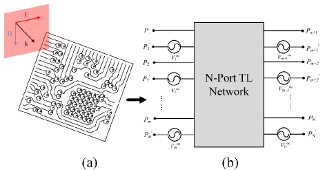
Figure 1: TL networks subject to (a) plane wave illumination and (b) its equivalent representation.
In Fig. 1 (b), V represents the open-circuit voltage at port m due to plane-wave illumination. Since coupling is a linear process, we can use the circuit shown in Fig. 2 to establish a connection between the external field and the open-circuit voltage. This circuit consists of an input impedance and a current-controlled voltage source. The voltage source V has the same waveform as the external excitation field. The input impedance at port m can be expressed as:
| (1) |
In (1), r represents the transresistance of the current-controlled voltage source, which is typically set to 1. However, to prevent Z from becoming numerically too small, the transresistance may be scaled to minimize numerical errors.
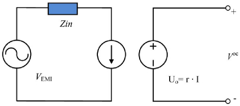
Figure 2: Circuit connected V and V.
Once we have established the connection between the V in Fig. 1 (b) and the external field with the circuit shown in Fig. 2, we will then get the circuit as shown in Fig. 3.
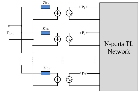
Figure 3: Extended (N+1)-port network, and external fields are fed from the (N+1)-port.
Network parameter analysis is widely used in circuit analysis. In this paper, we will treat the external field as an additional port. The open-circuit impedance representation of Fig. 3 is expressed by:
| (2) |
Then, the elements of the impedance matrix can be obtained with all the other ports left open-circuit:
| (3) |
Suppose the intrinsic Z-parameter of the TL network under consideration is:
| (4) |
(1) When iN and jN, since the (N+1) port is open circuit, the network parameters at these locations remain consistent with the intrinsic part.
(2) When i=N+1 and jN, the external fields are not affected by the parameters of the TL network, so the parameters for these positions are set to 0:
| (5) |
(3) When iN and j=N+1, which means all the ports are open-circuited except for the external one, then Zcan be obtained through a simple circuit analysis:
| (6) |
(4) When iN1 and jN1, then Z can be determined through a straightforward circuit analysis:
| (7) |
For N-port network illuminated by plane-wave, the extended Z-parameters can be expressed as:
| (8) |
When N2, the network extends to a three-port network, and the Z-parameter is written as:
| (9) |
So far, we have derived the extended Z-parameter. This can be translated into other network parameters, such as the Y-parameter or the S-parameter, which are typically presented in textual form. If the electromagnetic designer only needs to provide the results of the field analysis to the circuit designer, their task is considered complete at that point. As a black-box modeling method, most circuit solvers can identify network parameters, but they do not necessarily support the use of network parameters for circuit analysis directly, so it is necessary to introduce its circuit implementation.
As a robust numerical fitting method, VF employs N-order rational functions to fit transfer functions in the frequency domain [25–27], which denotes:
| (10) |
where sj signifies the complex frequency; r and p denotes the k-th residue and pole, respectively, with both being real or conjugate complex numbers; e and d represent linear and constant coefficients, respectively.
When residues and poles appear as conjugate complex numbers, the transfer function can be expressed as:
| (11) |
where and denote the real and imaginary parts of a complex number, respectively. Figure 4 illustrates a circuit implementation of the transfer function expressed in the impedance domain.
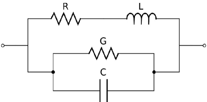
Figure 4: Equivalent circuit for conjugated residue and pole.
The impedance in Fig. 4 is given by:
| (12) |
By comparing (II.) and (12), the value of the lumped elements in Fig. 4 can be determined:
| (13) |
Although VF can be used to model multi-port networks, we recommend fitting the TL network and Z in Fig. 3 separately. This approach is more straightforward and allows for equivalent circuit modeling of TLs through alternative methods. For a more comprehensive understanding of TL network modeling methods, readers can refer to [28, 29].
A brief description of the (N1)-port black-box modeling is:
(1) Obtain the transfer function from full-wave simulation or measurement.
(2) Building an extended network incorporates external excitation interaction with the process in (2) to (10).
(3) Fitting the network parameters uses VF, while implementing the circuit employs lumped components.
(4) Performing the field-line coupling analysis in circuit solver.
III. VALIDATION STUDIES
A. Microstrip line terminal with nonlinear load
The first example involves a two-port network, with the detailed geometry shown in Fig. 5. It consists of a single MSL with a width of 1.5 mm, situated on a substrate with a dielectric constant of 2.2 and a thickness of 0.8 mm. The overall dimensions of the board are 8060 mm, and the thickness of the conductor layer is 35 m. A plane wave propagates along the z-axis, and the electric field is oriented along the x-axis.
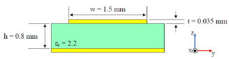
Figure 5: MSL section geometry diagram.
The excitation waveform is double exponential pulses, which is defined as the early time high-altitude electromagnetic pulse waveform in IEC 61000-2-9 [30], which is denoted as:
| (14) |
In this study, the parameters are set as E50 kV/m, k1.3, 410s, and 610 s, with the waveform shown in Fig. 6.
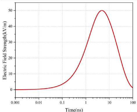
Figure 6: High-altitude electromagnetic pulse waveform in time domain.
To obtain the extended network parameters for this study, full-wave simulations were conducted to determine each element in the matrix. Subsequently, the input impedance Z and TL networks were fitted from 10 MHz to 10 GHz using VF. Figure 7 illustrates the fitting results of Z, while Fig. 8 presents the full-wave calculations and the fitting results of the S-parameters of the TL, demonstrating good agreement between them.
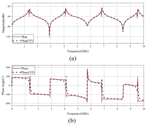
Figure 7: (a) Amplitude and (b) phase of the input impedance (Z) of port 1, with the dashed line representing the VF results.
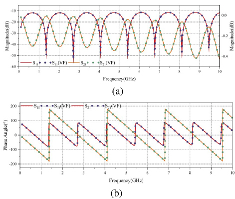
Figure 8: (a) Amplitude and (b) phase response of the MSL corresponding to the geometry shown in Fig. 5. The dashed lines represent the vector fitting (VF) results.
After the network parameters are determined and the circuit is implemented, their effectiveness is verified. In the validation example, port 1 is connected to a 50 resistor, while port 2 is connected to a nonlinear diode, with its equivalent circuit depicted in Fig. 9, and the nonlinear IV equation of the diode is:
| (15) |
where I 510A signifies the reverse saturation current, T300 K, e denotes the elementary charge, and k represents the Boltzmann constant.
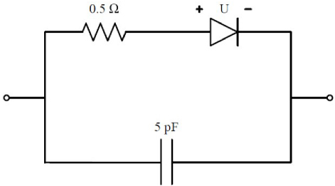
Figure 9: Equivalent circuit of the diode.
Figure 10 shows the calculation results of the full-wave and extended network parameters, and the two agree well. Note that the peak occurrence time of the induced voltage does not coincide with that of the excitation voltage.
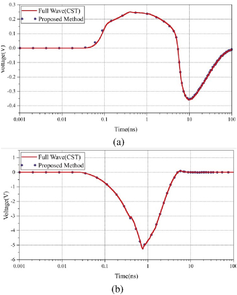
Figure 10: Induced voltage on (a) resistor and (b) diode.
B. MSLs with multi-ports
In general, TL networks are more of a concern in the EMC community or industry. In this example, a network with five-port is studied. Figure 11 shows the detailed geometry, four-port are connected between the MSL termination and the reference ground plane, with one-port spanning MSLs. This configuration is more realistic and closely resembles a typical PCB layout.
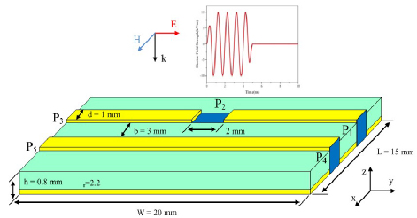
Figure 11: Pair of microstrip lines exposed to plane-wave illumination.
The impressed electric field, as shown in Fig. 11, consists of a plane wave incident normal to the ground plane, with the electric field aligned along the TL axis. The incident waveform is considered as a narrowband HPM [31], illustrated in (16):
| (16) |
where E denotes the peak electric field strength; signifies the pulse width; t and trepresent the rise time and fall time, respectively; f is the carrier frequency of the HPM pulse. In the following example, E10 kV/m, 4 ns, tt0.5 ns.
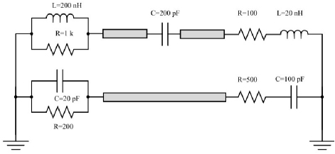
Figure 12: Schematic of port configuration.
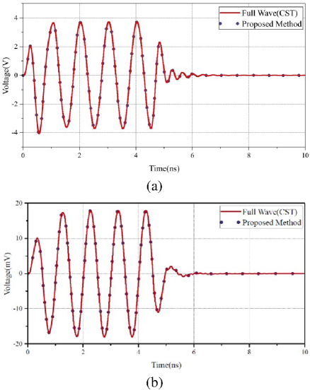
Figure 13: Induced voltage at different loads: (a-e) represent the induced voltages on ports 1-5, respectively.
Once again, we need to extract the extended network parameters and implement the circuit. For the sake of brevity, we will not present this section in detail. Instead, we will show the results obtained from both full-wave simulations and this method when the port is terminated with various loads. Figure 13 shows the induced voltage for each load in the circuit configuration shown in Fig. 12. It can be observed that the full-wave calculations are consistent with the method presented in this paper. The value of the induced voltage depends on the type and value of the load. Due to the presence of the energy storage element, the induced voltage does not immediately return to zero after the pulse ends, as discussed in detail in [3].
C. MSL in perforated metallic enclosure
To resist the threat of HPEM, designers often use metal enclosures to protect the internal circuitry, however, due to the need for ventilation or wiring, there will be some slots or apertures in the cavity, which degrades the shielding ability of the cavity. Therefore, we need to evaluate the immunity of circuits in a perforated metallic enclosure. In this example, a two-port TL located in a perforated enclosure as shown in Fig. 14 is considered.
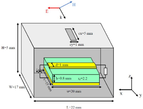
Figure 14: Schematic of the two-port circuit illuminated by IEMI source.
In this example, the enclosure dimensions LWH are 22175 mm, and the dimensions of the perforated rectangular aperture are cxcy51 mm. The substrate measures abc20150.8 mm with a dielectric constant of 2.2. The length and width of the MSL are 20 mm and 1 mm, respectively. The TL is then illuminated by a plane wave with the propagation direction k(0, 0.154, -0.988), which deviates slightly from the z-axis. The waveform is a Gaussian waveform, as shown in Fig. 15.
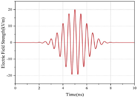
Figure 15: Time domain representation of incident Gaussian waveform.
The expression for the waveform is given as:
| (17) |
where E20 kV/m, 1 ns, f2 GHz and t5 ns. Port 1 is connected to a 2 GHz rectangular pulse current source, and port 2 is connected to a 50 resistor. It can be regarded as a clock signal in a digital system. Figure 16 shows the signal on the resistor. The method described in this paper is consistent with the full-wave results. Additionally, we observe that the signal undergoes significant distortion under the illumination of an external field.
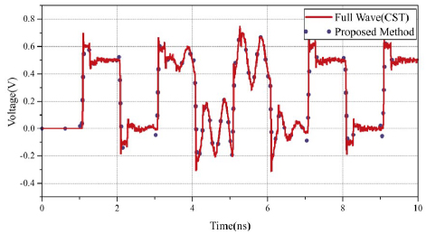
Figure 16: Induced voltage on the resistor.
IV. DISCUSSION
In this work, we have developed an extended network parameter to model TL under external field illumination. The following discussion highlights several key issues that need to be addressed.
(1) In general, the coverage of network parameters should cover the frequency band we are interested in. In the case of the presence of nonlinear loads, the influence of harmonics should also be considered. The extraction range of network parameters should cover as many harmonics as possible.
(2) The simulation may encounter convergence issues due to the model being established within a finite bandwidth, which can result in non-causal responses. Relevant solutions can be found in [19]. Additionally, circuit convergence can be affected by the violation of passivity in the macromodel. Thus, during vector fitting, the passivity of the model should be ensured.
(3) In this paper, we have introduced the Z-parameters, through which we observe the clear influence of external fields. However, S-parameters are supported by a broader range of circuit solvers. Certain simulation software, like ADS, facilitates direct frequency domain analysis using S-parameters. In some instances, using a circuit file, such as a SPICE netlist, may be more suitable for compatibility reasons, as it is widely supported.
(4) The last issue is its applicability. Although this paper mainly focuses on MSLs, the theory can also be generalized to other types of TLs, such as cables. In addition, in the verification section of the paper, electromagnetic data primarily originates from full-wave simulations. As mentioned earlier, electromagnetic data can also be obtained through measurements using a network analyzer test in an electromagnetic anechoic chamber or a transverse electromagnetic cell.
V. CONCLUSION
In this study, extended network parameters were proposed and applied for the analysis of TLs under external field irradiation. We demonstrated their effectiveness through three examples, involving both shielded and unshielded scenarios, linear and nonlinear loads, as well as single TL and TL networks. The simulation results from the circuit were consistent with the full-wave simulation results but required less computation time. The extended network parameters incorporate the influence of external fields, enabling the analysis of field-line coupling problems within the circuit solver without the need for repeated field calculations. Furthermore, this method facilitates a direct connection between the electromagnetic solver and the circuit solver, allowing the export of electromagnetic calculation results to the circuit solver. This approach is particularly suitable for large-scale projects that necessitate collaborative design efforts among multiple designers in the realm of electromagnetic and circuits.
ACKNOWLEDGMENT
This work was supported in part by the National Natural Science Foundation of China under Grant 61921002.
REFERENCES
[1] D. V. Giri, R. Hoad, and F. Sabath, “Implications of high-power electromagnetic (HPEM) environments on electronics,” IEEE Electromagnetic Compatibility Magazine, vol. 9, no. 2, pp. 37-44, 2020.
[2] W. A. Radasky and R. Hoad, “Recent developments in high power EM(HPEM) standards with emphasis on high altitude electromagnetic pulse (HEMP) and intentional electromagnetic interference (IEMI),” IEEE Letters on Electromagnetic Compatibility Practice and Applications, vol. 2, no. 3, pp. 62-66, 2020.
[3] R. Michels, M. Kreitlow, A. Bausen, C. Dietrich, and F. Gronwald, “Modeling and verification of a parasitic nonlinear energy storage effect due to high-power electromagnetic excitation,” IEEE Transactions on Electromagnetic Compatibility, vol. 62, no. 6, pp. 2468-2475, 2020.
[4] C. Pouant, J. Raoult, and P. Hoffmann, “Large domain validity of MOSFET microwave-rectification response,” in 2015 10th International Workshop on the Electromagnetic Compatibility of Integrated Circuits (EMC Compo), pp. 232-237, 10-13 Nov. 2015.
[5] T. Dubois, J. J. Laurin, J. Raoult, and S. Jarrix, “Effect of low and high-power continuous wave electromagnetic interference on a microwave oscillator system: From VCO to PLL to QPSK receiver,” IEEE Transactions on Electromagnetic Compatibility, vol. 56, no. 2, pp. 286-293, 2014.
[6] Y. Bayram, J. L. Volakis, S. K. Myoung, S. J. Doo, and P. Roblin, “High power EMI on RF amplifier and digital modulation schemes,” IEEE Transactions on Electromagnetic Compatibility, vol. 50, no. 4, pp. 849-860, 2008.
[7] J. E. Baek, Y. M. Cho, and K. C. Ko, “Damage modeling of a low-noise amplifier in an RF front-end induced by a high-power electromagnetic pulse,” IEEE Transactions on Plasma Science, vol. 45, no. 5, pp. 798-804, 2017.
[8] Q. S. Liang, C. C. Chai, H. Wu, Y. Q. Liu, F. X. Li, and Y. T. Yang, “Mechanism analysis and thermal damage prediction of high-power microwave radiated CMOS circuits,” IEEE Transactions on Device and Materials Reliability, vol. 21, no. 3, pp. 444-451, 2021.
[9] M. G. Backstrom and K. G. Lovstrand, “Susceptibility of electronic systems to high-power microwaves: Summary of test experience,” IEEE Transactions on Electromagnetic Compatibility, vol. 46, no. 3, pp. 396-403, 2004.
[10] C. R. Paul, “Frequency response of multiconductor transmission lines illuminated by an electromagnetic field,” IEEE Transactions on Electromagnetic Compatibility, vol. EMC-18, no. 4, pp. 183-190, 1976.
[11] F. Rachidi, “A review of field-to-transmission line coupling models with special emphasis to lightning-induced voltages on overhead lines,” IEEE Transactions on Electromagnetic Compatibility, vol. 54, no. 4, pp. 898-911, 2012.
[12] Q. F. Liu, C. Ni, H. Q. Zhang, and W. Y. Yin, “Lumped-network FDTD method for simulating transient responses of RF amplifiers excited by intentional electromagnetic interference signals,” IEEE Transactions on Electromagnetic Compatibility, vol. 63, no. 5, pp. 1512-1521, 2021.
[13] W. Rui and J. Jian Ming, “Incorporation of multiport lumped networks into the hybrid time domain finite-element analysis,” IEEE Transactions on Microwave Theory and Techniques, vol. 57, no. 8, pp. 2030-2037, 2009.
[14] X. Wang, A. Huang, W. Zhang, R. Yazdani, D.-H. Kim, and T. Enomoto, “Methodology for analyzing coupling mechanisms in RFI problems based on PEEC,” IEEE Transactions on Electromagnetic Compatibility, vol. 65, no. 3, pp. 761-769, 2023.
[15] H. H. Zhang, L. J. Jiang, and H. M. Yao, “Embedding the behavior macromodel into TDIE for transient field-circuit simulations,” IEEE Transactions on Antennas and Propagation, vol. 64, no. 7, pp. 3233-3238, 2016.
[16] T. Wendt, M. D. Stefano, C. Yang, S. Grivet-Talocia, and C. Schuster, “Iteration dependent waveform relaxation for hybrid field nonlinear circuit problems,” IEEE Transactions on Electromagnetic Compatibility, vol. 64, no. 4, pp. 1124-1139, 2022.
[17] T. Liang, G. Spadacini, F. Grassi, and S. A. Pignari, “Worst-case scenarios of radiated-susceptibility effects in a multiport system subject to intentional electromagnetic interference,” IEEE Access, vol. 7, pp. 76500-76512, 2019.
[18] F. Vanhee, D. Pissoort, J. Catrysse, G. A. E. Vandenbosch, and G. G. E. Gielen, “Efficient reciprocity-based algorithm to predict worst case induced disturbances on multiconductor transmission lines due to incoming plane waves,” IEEE Transactions on Electromagnetic Compatibility, vol. 55, no. 1, pp. 208-216, 2013.
[19] J. T. Williams, L. D. Bacon, M. J. Walker, and E. C. Zeek, “A robust approach for the analysis of EMI/EMC problems with nonlinear circuit loads,” IEEE Transactions on Electromagnetic Compatibility, vol. 57, no. 4, pp. 680-687, 2015.
[20] A. Kalantarnia, A. Keshtkar, and A. Ghorbani, “Predicting the effects of HPEM radiation on a transmission line terminated with linear/nonlinear load in perforated metallic enclosure using FDDM/VF,” IEEE Transactions on Plasma Science, vol. 48, no. 3, pp. 669-675, 2020.
[21] D. Winklestein, M. B. Steer, and R. Pomerleau, “Simulation of arbitrary transmission line networks with nonlinear terminations,” IEEE Transactions on Circuits and Systems, vol. 38, no. 4, pp. 418-422, 1991.
[22] J. E. Schutt Aine and R. Mittra, “Scattering parameter transient analysis of transmission lines loaded with nonlinear terminations,” IEEE Transactions on Microwave Theory and Techniques, vol. 36, no. 3, pp. 529-536, 1988.
[23] K. S. Kundert and A. Sangiovanni Vincentelli, “Simulation of nonlinear circuits in the frequency domain,” IEEE Transactions on Computer Aided Design of Integrated Circuits and Systems, vol. 5, no. 4, pp. 521-535, 1986.
[24] Y. Bayram and J. L. Volakis, “Hybrid S-parameters for transmission line networks with linear/nonlinear load terminations subject to arbitrary excitations,” IEEE Transactions on Microwave Theory and Techniques, vol. 55, no. 5, pp. 941-950, May 2007.
[25] B. Gustavsen and A. Semlyen, “Rational approximation of frequency domain responses by vector fitting,” IEEE Transactions on Power Delivery, vol. 14, no. 3, pp. 1052-1061, 1999.
[26] B. Gustavsen, “Improving the pole relocating properties of vector fitting,” IEEE Transactions on Power Delivery, vol. 21, no. 3, pp. 1587-1592, 2006.
[27] B. Salarieh and H. M. J. De Silva, “Review and comparison of frequency-domain curve-fitting techniques: Vector fitting, frequency-partitioning fitting, matrix pencil method and loewner matrix,” Electric Power Systems Research, vol. 196, 2021.
[28] B. Gustavsen and A. Semlyen, “Admittance-based modeling of transmission lines by a folded line equivalent,” IEEE Transactions on Power Delivery, vol. 24, no. 1, pp. 231-239, 2009.
[29] A. Dounavis, R. Achar, and M. Nakhla, “A general class of passive macromodels for lossy multiconductor transmission lines,” IEEE Transactions on Microwave Theory and Techniques, vol. 49, no. 10, pp. 1686-1696, 2001.
[30] IEC 61000-2-9, Electromagnetic Compatibility (EMC) – Part 2-9: Description of HEMP Environment — Radiated Disturbance, 1996.
[31] J. Benford, J. A. Swegle, and E. Schamiloglu, High Power Microwaves. Boca Raton, Florida: CRC Press, 2015.
BIOGRAPHIES

Mingwen Zhang received the B.S. and M.S. degrees in electronic science and technology from University of Electronic Science and Technology of China (UESTC), Chengdu, China, in 2017 and 2020, respectively. He is pursuing the Ph.D. degree with UESTC, Chengdu, China. His research interests include electromagnetic interference and microelectronic reliability.

Chunguang Ma received the B.S. degree in physics from Anqing Normal University, Anqing, China, in 2008, and the Ph.D. degree in plasma physics from the University of Electronic Science and Technology of China (UESTC), Chengdu, China, in 2015. He was with the College of Engineering, University of Connecticut, Storrs, CT, USA, as a Visiting Researcher, from 2013 to 2014. He was with the School of Physical Electronics, UESTC, as a Lecturer, from 2015 to 2018. He is with the School of Electronic Science and Engineering, UESTC, as an Associate Researcher. His research interests include electromagnetic compatibility and interference, microwave and millimeter wave devices, circuits and systems, and ultra-wideband radar systems.

Bicheng Zhang received the B.S. degree in Electronic and Information Engineering from University of Electronic Science and Technology of China (UESTC), Chengdu, China, in 2024. He is pursuing the M.S. degree with UESTC. His research interests include electromagnetic interference and electromagnetic coupling.

Yong Luo received the Ph.D. degree in physical electronics from the University of Electronic Science and Technology of China (UESTC), Chengdu, China, in 2003. Since 1988, he has been with the Optoelectronics Center, UESTC, where he has been a Professor with the School of Physical Electronic, since 1999. He is also a researcher of with the Laboratory of Electromagnetic Space Cognition and Intelligent Control, Beijing, China. His research interests include gyrotron traveling-wave tube, high-power millimeter-wave technology and its application.
ACES JOURNAL, Vol. 40, No. 4, 340–349
doi: 10.13052/2024.ACES.J.400408
© 2025 River Publishers