A Novel Compact and Lightweight Harmonic Tag for Insect Tracking
Zhan-Fei Su, Xian-Rong Wan∗, Jian-Xin Yi, Zi-Ping Gong, and Zi-Yao Wang
College of Electronic Information
Wuhan University, Wuhan, 430072, China
zfsu333@whu.edu.cn, xrwan@whu.edu.cn, jxyi@whu.edu.cn,
zpgong@whu.edu.cn, qlzywzy@whu.edu.cn
*Corresponding Author
Submitted On: February 22, 2025; Accepted On: June 28, 2025
ABSTRACT
Harmonic radar sensor systems is a special wireless sensor system that has been used in insect tracking in recent years due to its excellent anti-clutter capability. Generally, a harmonic radar sensor systems consists of a radar transceiver and a specially designed harmonic tag. However, tags tend to become entangled with vegetation in insect tracking experiments. This paper proposes a strong echo signal and miniaturized low-mass passive tag design method, which targets Internet-of-Things insect tracking applications. We introduce foldable structures in antenna designing with advanced non-linear selection criterion under the unified frequency operation environment. The conversion loss (CL) of the tag is not impacted by the measures taken to minimize its mass and size. The results using both simulated and real data demonstrate remarkable improvements in size of tags, weight of tags, and echo signal strength of tags within our proposed method on the passive tags. The effectiveness of the method is verified by the results of harmonic radar illuminate tag. This work possesses the advantages of a low profile, lightweight design, strong echo signal, and compact dimensions.
Index Terms: Compact size, frequency doubler, harmonic radar, harmonic tag, harmonic transponder, radio frequency identification (RFID), tag antenna.
I. INTRODUCTION
With the widespread adoption of the Internet of Things (IoT) and wireless sensor networks in everyday life, Radio Frequency Identification (RFID) has become an increasingly important technology for tagging, tracking, sensing, and locating objects [1-5]. Traditional RFID systems rely on a single frequency for both querying and responding, which can result in unwanted self-interference or clutter noise caused by environmental reflections. In contrast, sensor systems based on harmonic radar and transponders provide an attractive solution to these challenges. In this approach, the radar queries the tag at the fundamental frequency, and the tag attached to the target reflects higher-order harmonics, which the radar system can detect. In most cases, these transponders operate at the second harmonic frequency.
Harmonic radar sensor systems were first explored over 50 years ago and have since undergone rapid development [6]. Due to its high robustness against radar clutter interference, harmonic radar-based sensor systems have found applications in a variety of scenarios, such as search and rescue operations [7], temperature and humidity measurements [8], vital signs detection [9], wireless liquid sensing [10], indoor equipment detection [11], and object detection [12], among others. In the late 20th century, harmonic radar and transponder systems attracted the attention of entomologists due to their exceptional anti-interference capabilities, leading to their use in insect tracking [13]. In the application of harmonic radar for insect tracking, the design of insect harmonic tags is one of the key technologies. The system’s working principle is illustrated in Fig. 1.
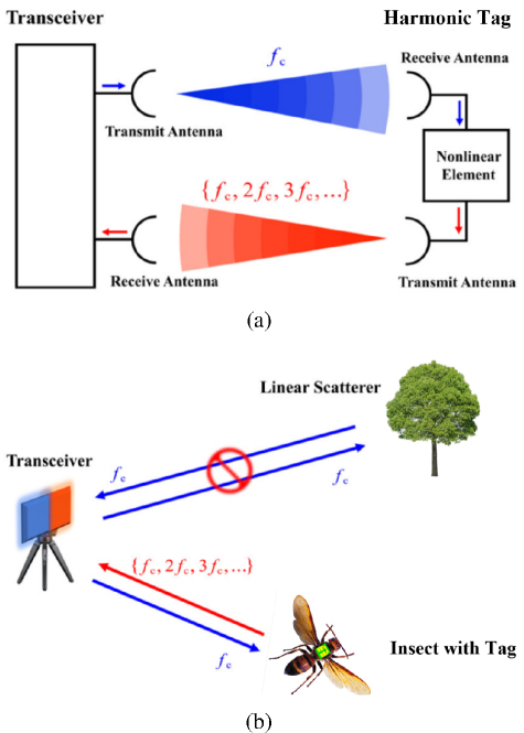
Figure 1: Schematic of the harmonic radar system. (a) The composition of a harmonic radar. represents the fundamental carrier frequency. (b) Working principle of harmonic radar. Blue lines represent the signals with the fundamental carrier frequency. Red lines represent the signals with the harmonic carrier frequency. Linear scatterer echo usually does not contain nonlinear frequency components, so it will not be detected by harmonic radar.
In insect tracking applications, the harmonic tag attached to the insect receives the fundamental frequency signal transmitted by the harmonic radar and generates a second harmonic signal, which is propagated back to the harmonic radar’s receiver, allowing the insect’s position to be determined. Mascanzoni and Wallin used tags consisting of a monopole antenna and a diode to track beetles [13]. The shape of the tag is like a whip and is placed on the beetle’s body. The harmonic radar successfully detected the insect. Brazee et al.’s tracking of weevils using similar tag [14] also succeeded. In [15], the dipole ring tag designed by Colpitts and Boiteau, has improved the detection range compared to the monopole tag [16]. Its structure is composed of dipole antenna(copper wire), inductance coil and Schottky diode. Similar tags are also mentioned in literature [17], with a “J” shape design. However, experiments tracking bees found tag height makes it difficult for insects to enter or leave the rearing box. Riley and Smith addressed this problem by installing tags on insects when they leave the rearing box [18] and removing them when the insects return to the box. On the other hand, Capaldi found that the insect body caused electromagnetic field distortion [19], resulting in a decrease in antenna efficiency [18]. Milanesio et al. introduced a disc for installing tags [20], alleviating this problem. These tag designs were successfully tested in experiments. However, the disadvantages include low conformity to insect body, difficulties in attaching the tag, and making it mechanically robust. Meanwhile, in insect tracking experiments, the tags may get entangled in vegetation or become difficult to move in and out of nests, which can lead to tag deformation and reduce their performance.
Therefore, to reduce the impact of the tags on insect activity and improve their reliability, it is necessary to design low-profile tags. With the tag processing technology mature, printed tags are increasingly used in harmonic radar experiments to track insects. The harmonic tag in literature[21] utilizes a Minkowski fractal structure, which effectively enhances the tag’s gain. Lavrenko improved the matching method of traditional dipole tags [22] by combining the printed matching inductor circuit with a linear antenna, reducing the flying resistance of insects. Kiriazi designed the tags with a butterfly knot topology [23] to facilitate the movement of snails. Tsai introduced composite left and right transmission line tags [24], which use a short-circuit pillar structure, improving performance. Although existing printed tags have achieved a low-profile structure, their size and weight still require further improvement. The tag described in literature [25] reduced its size, however, to achieve the desired weight and dimensions, the operating frequency of the tag needs to be raised to higher frequencies. This means lower detection range and increased price of radar modules. Therefore, designing an ideal miniaturized tag that does not compromise conversion gain remains a challenge.
To address this challenge, this paper proposes a compact and lightweight passive tag design methodology. The approach employs a folded antenna topology to reduce the tag’s size, while utilizing polyimide (PI) as the substrate material. This reduces the tag’s mass and enables a low-profile structure. The effectiveness of the proposed method is validated through simulations and experimental data, with comparisons made to existing designs.
The main contributions of this article are summarized as follows.
The mechanism of harmonic generation in nonlinear devices is theoretically analyzed. Simulations are performed to assess the impact of different nonlinear devices on conversion loss (CL), and theoretical calculations confirm the consistency of the simulation results.
The conventional formula for calculating the reflection coefficient () of harmonic tags is revised to address physical inconsistencies observed under certain conditions, such as values exceeding unity. The proposed formula eliminates these limitations and provides a more accurate metric for assessing impedance matching between the tag antenna and the nonlinear load.
A folded antenna topology is designed, where the radiating element is folded into a square pattern. This reduces the physical size of the tag antenna while maintaining its effective electrical length. Compared to traditional linear or other folded geometries, this design improves spatial efficiency, enabling tag miniaturization. Additionally, the effect of increasing the patch width on the tag’s radiation performance is analyzed. A wider patch enhances the current distribution area on the radiating surface, which is directly correlated with improved antenna gain.
The structure of this paper is organized as follows. Section II discusses the analysis and simulation of the tag model, including the mechanism of harmonic generation by diodes, methods for selecting nonlinear components, and the correction of the complex power wave reflection coefficient formula for tag antennas. Section III delves into the analysis and design of the tag, presenting simulation comparisons between the square topology and other structures for reducing tag size, the effect of patch width on current distribution across the radiation surface, and the impact of different matching techniques on tag antenna performance. Section IV focuses on the experimental testing of the tags. Finally, section V concludes with the main findings.
II. TAG MODEL ANALYSIS AND SIMULATION
The tag consists of nonlinear components, a tag antenna, and a matching circuit. Tags suitable for insect tracking should possess characteristics such as low CL, small size, low air resistance, and strong echo signal. Selecting appropriate nonlinear components, such as multiplier devices, to generate harmonic carrier signals for the tag is essential for minimizing tag CL. Additionally, this paper designs a passive tag antenna with a folding structure, achieving tag miniaturization and size reduction. Moreover, the intensity of the echo signal received by the harmonic radar determines its detection range. To ensure efficient energy transmission between the nonlinear components and the tag antenna, a matching circuit must be designed to ensure optimal energy transfer.
A. Theoretical analysis of nonlinear components
Various active or passive nonlinear components can generate harmonic signals for tags, including diodes [26,27], nonlinear transmission lines [28,29], transistors [30,31], and phase-locked loops [32]. When comparing factors such as operating frequency, harmonic factor, size, and power requirements, diodes emerge as the optimal choice as multipliers for passive tags [33].
The tag antenna intercepts signals from the harmonic radar, inducing a voltage that drives the diode by generating current. Owing to the inherent properties of the diode, it can alter the state of the initial current, resulting in the production of current containing harmonic signals. The precise alterations in the operational state are depicted in Fig. 2. The left panel of Fig. 2 illustrates the relationship between induced voltage and time before passing through the diode. Upon reaching the threshold voltage required to activate the diode, the operational state of the tag antenna corresponds to the representation in the right panel of Fig. 2. Subsequently, the voltage amplitude is halved, and the tag antenna produces various harmonic frequencies, including the 2nd and 3rd harmonics. This phenomenon arises from the exponential relationship between the diode’s voltage-current (V-I) characteristic, illustrated in the central diagram of Fig. 2. Passage of the signal through the diode induces nonlinear distortion of the input signal, leading to a frequency-doubling phenomenon.
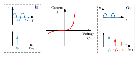
Figure 2: Diode frequency doubling phenomenon.
The theoretical analysis is as follows, the Schottky equation for the diode in small signal operation is given by [34]:
| (1) |
Where is the current through the diode, is the reverse saturation current of the diode, is the ideality factor, is the thermal voltage, and is the voltage across the diode.
In equation (1), when = 0, the equation can be expanded using Taylor series as:
| (2) |
The voltage source provided to the diode in the tag is the induced voltage on the tag antenna, which can be equivalent to a sine signal:
| (3) |
In equation (3), A represents the amplitude of the junction voltage, 2, denotes the frequency of the fundamental signal.
Periodic signals that satisfy the Dirichlet conditions can be represented by the Fourier series as a combination of such signals. Substituting equation (4) into equation (2) yields:
| (4) |
From equation (5), it can be observed that the current through the Schottky diode contains signals with frequencies that are multiples of the fundamental frequency 2, and expanding further will yield harmonic signals of the 3rd order and above.
Classical p–n junction diodes have high junction capacitance, rendering them unsuitable for high-frequency applications. Conversely, Schottky diodes, formed by metal-semiconductor contacts, exhibit lower junction capacitance, rendering them suitable for high-frequency operation [34]. However, Schottky diodes, being hot carrier diodes, typically exhibit a reverse saturation current on the order of 10-6 A, whereas for other diode types, the reverse saturation current is typically on the order of 10-14 A. Consequently, Schottky diodes are more suitable than other diode types as nonlinear components in RF harmonic tags.
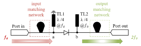
Figure 3: The schematic diagram of the harmonic tag.
B. Analysis of the dynamic equivalent model of nonlinear components
Figure 3 illustrates the circuit schematic of a traditional dual-port passive harmonic transponder, along with the energy flow paths for the fundamental wave and the second harmonic. The red arrows represent the energy flow path of the fundamental wave, while the green arrows indicate the energy flow path of the second harmonic. To enhance the nonlinear conversion process in the diode, quarter-wavelength short-circuited and open-circuited stubs (denoted as TL1 and TL2, respectively) are placed around the diode [35]. The quarter-wavelength short-circuited stub TL1 at the input acts as an open circuit at the fundamental frequency , allowing the injected fundamental signal to reach the diode. However, at the second harmonic frequency 2, TL1 behaves as a short circuit, grounding the second harmonic at point a. On the output side, the quarter-wavelength open-circuited stub TL2 acts as a short circuit at the fundamental frequency , thereby shorting the fundamental signal while minimally affecting the second harmonic. This is because, at , the open-circuited stub is a quarter-wavelength long, but at 2, it becomes a half-wavelength long, maintaining an open-circuit condition at 2. Consequently, the fundamental signal is short-circuited and reflected at point b.
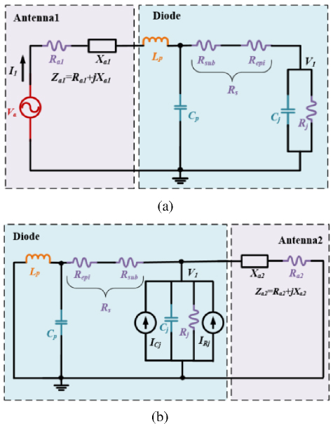
Figure 4: Nonlinear transformation schematic model. (a) Fundamental frequency. (b) Harmonic frequency.
The injected RF signal at the fundamental frequency passes through the input matching network and reaches the diode’s input terminal. Meanwhile, the quarter-wavelength open-circuited stub on the output side shorts the fundamental signal at . Nonlinear transformation schematic model at is depicted in Fig. 4 (a). At the second harmonic frequency 2, the short-circuited and open-circuited stubs function as a short circuit and an open circuit, respectively. At this point, the diode acts as a generator for second harmonic energy. Due to the stubs and the output matching network designed for 2, maximum second harmonic power is delivered to the output port. Nonlinear transformation schematic model at 2 is shown in Fig. 4 (b).
To simplify the analysis, the input and output matching networks are omitted in Fig. 4. The diode is represented using the Shockley model, which includes the junction resistance , junction capacitance , and series resistance , the latter comprising the epitaxial layer resistance and substrate resistance [18]. Parasitic capacitance and parasitic inductance are used to model the packaging effects. The fundamental RF signal source in Fig. 4 (a) is represented by a Thévenin equivalent circuit, while the diode, acting as the second harmonic signal source in Fig. 4 (b), is modeled using a Norton equivalent circuit. Additionally, represents the node voltage. The SPICE parameters of the diode, sourced from SKYWORKS, Central Semi and AVAGO Technologies, are listed in Table 1.
The working principle of the tag is illustrated in Fig. 4. In Fig. 4 (a), the radiation resistance and reactance of the tag’s fundamental frequency antenna are denoted as and , respectively. The antenna receives the fundamental signal transmitted by the harmonic radar’s transmit antenna, generating current and voltage , which deliver energy to the diode. In Fig. 4 (b), the radiation resistance and reactance of the harmonic antenna are represented as and , respectively. The diode’s junction resistance () and capacitance () produce currents and , which contain harmonic components. These currents radiate electromagnetic waves through the tag’s harmonic antenna, reflecting back to the harmonic radar’s receive antenna.
Table 1: The main SPICE parameters of the diode
| Parameter | SMS 7630 | CDC 7630 | HMPS 2820 | HSMS 2850 |
| (pF) | 0.14 | 0.40 | 0.50 | 0.50 |
| 0.40 | 0.40 | 0.50 | 0.50 | |
| (V) | 0.34 | 0.34 | 0.65 | 0.35 |
| () | 20.00 | 51.00 | 8.00 | 25.00 |
| (A) | 5e-6 | 3.8e-6 | 2.2e-8 | 3e-6 |
| 1.05 | 1.05 | 1.08 | 1.06 | |
| (A) | 1e-4 | 1e-4 | 1e-4 | 3e-4 |
| (V) | 2.00 | 2.00 | 15.00 | 3.80 |
| (eV) | 0.69 | 0.69 | 0.60 | 0.69 |
| (pF) | 0.16 | 0.16 | 0.08 | 0.08 |
| (nH) | 0.07 | 0.07 | 2.00 | 2.00 |
As described in [36], the theoretical model’s validity and accuracy can be verified by comparing theoretical calculations with simulation results, enabling the optimization of diode selection and circuit design. To comprehensively evaluate the diode’s CL characteristics, this study employs a combined approach of theoretical formula calculations and software simulations.
The fundamental current can be written as:
| (5) |
where is the Bessel function of first kind of order . The injecting current can be obtained by applying the Kirchhoff Circuit Laws considering the effect of the packaging components
| (6) |
The injecting voltage can be expressed by
| (7) |
The injecting power can be calculated by
| (8) |
The second-harmonic current due to the junction resistance can be calculated by
| (9) |
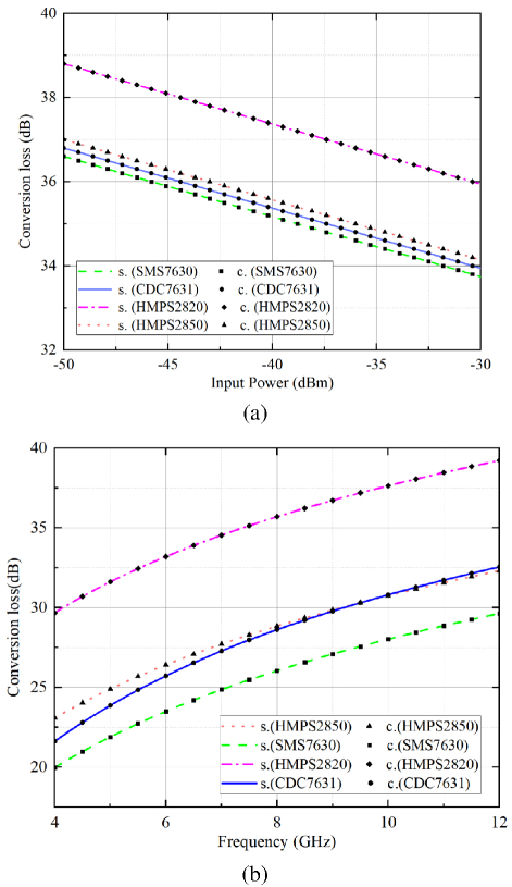
Figure 5: Comparison of calculated and simulated CL performance of four typical selected diode-based tag. (a) The injecting power is in a range of -50 to -30 dBm. (b) Operating frequency in the range of 4 to 12 GHz.
The generated second-harmonic current can be expressed by
| (10) |
The current coming out of the diode can be written by
| (11) |
where is the output impedance equal to the complex conjugate of the packaged diode’s impedance in order to maximize the power transfer to the output port. Then, the generated second harmonic power reaching the output can be expressed by
| (12) |
The can be expressed by
| (13) |
Using the SPICE parameters of the diodes, several commonly used diodes were selected for validation. During the validation process, the input power was swept from -50 dBm to -30 dBm. The harmonic balance simulation results for each diode-based transponder, along with the calculated CL values as a function of input power, are shown in Fig. 5 (a). Additionally, a frequency sweep was performed over the range of 4–12 GHz, and the relationship between frequency and is depicted in Fig. 5 (b).
It is evident from both figures that the simulation results from the harmonic balance simulator are consistent with the calculated values. Based on these results, it can be concluded that within the power and frequency range of interest, the diode SMS-7630 exhibits superior performance compared to the other diodes.
C. Improved calculation method for tag antenna reflection coefficient
In tag optimization, impedance matching has long been recognized as one of the key factors for achieving optimal tag performance. To maximize power transfer, the input impedance of the diode connected to the antenna must be conjugate-matched to the antenna’s impedance. The reflection coefficient (), as observed in tag antenna simulations and reflects the matching relationship between the tag antenna and the diode. Lower values of generally indicate higher radiation efficiency.
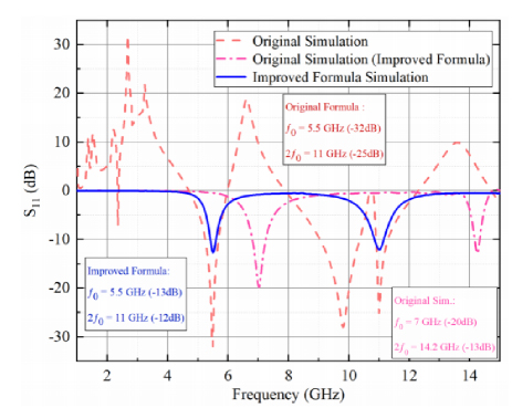
Figure 6: Comparison of the reflection coefficient () before and after formula correction.
Although a loop diameter of 1 mm is a common choice for linear dipole tags [22], no simulation analysis currently substantiates this choice. However, with a reference impedance of 50 ohms, the reflection coefficient () obtained from finite element simulation software often exceed 0 dB. This discrepancy can be attributed to the following reasons.
The reflection coefficient () can be expressed as [37]:
| (14) | |
| (15) |
The diode impedance can be expressed as , the tag antenna impedance can be expressed as , substituting the values into the equation, we obtain:
After expanding the equation:
| (17) |
After simplification:
| (18) |
The final expression can be written as:
| (19) |
When the reactance is smaller than of the input resistance, the simulated reflection coefficient () can take values exceeding the physically possible range, resulting in unrealistic results. The result is shown in Fig. 6, where the pink dashed line represents this phenomenon (while the curve derived using the improved formula is shown by the red dashed line in Fig. 6, which exhibits an offset compared to the pink dashed line from the Original Simulation). Therefore, the method for calculating the reflection coefficient needs to be improved.
It needs to be corrected to the complex power wave reflection coefficient as:
| (20) |
This allows the traditional reflection coefficient curve to be used to describe the impedance matching between the tag antenna and the diode. The simulated reflection coefficient using the improves formula is shown by the solid blue line in Fig. 6. To verify the effectiveness of the proposed method, a tag was fabricated based on the unmodified reflection coefficient () calculation method, as shown in Fig. 20 (a).
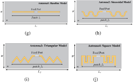
Figure 7: Four different topology dipole antennas. (a) Baseline. (b) Sinusoidal. (c) Triangular. (d) Square.
III. TAG ANALYSIS AND DESIGN
A. Analysis of folding topology structure
The common antenna topology used in insect tags is the dipole antenna, primarily due to its simple structure, ease of fabrication, moderate size, and high radiation efficiency. However, its relatively large size can impact the mobility of the insect [38]. The goal of this paper is to design a square meander-line antenna, clearly demonstrating the small-size design concept of a folded antenna, and compare its performance with two other meander-line designs: sinusoidal and triangular. To maintain structural consistency, these three meander-line designs are based on the traditional baseline dipole antenna design as a template. All three designs were simulated using electromagnetic field simulation software based on the finite element method (FEM), and their performance was compared in terms of size reduction, actual gain, reflection coefficient, and bandwidth.
For ease of comparison, all antennas (Antenna1-Antenna4) use the same dielectric substrate (PI), width , and driver patch width as shown in Fig. 7. Antenna 1 is the baseline dipole model, maintaining the original topology of the dipole antenna, with a patch length Patch_l1 and a dielectric substrate length ; Antenna 2 is the Sinusoidal Model, with a patch length Patch_l2 and dielectric substrate length ; Antenna 3 is the Triangular Model, with a patch length Patch_l3 and dielectric substrate length ; and Antenna 4 is the Square Model, with a patch length Patch_l4 and dielectric substrate length . Their size comparisons are shown in Table 2. The simulation results optimized using the software are shown in Fig. 8, with a center operating frequency of 5.5 GHz. Any further changes to their dimensions would result in a frequency shift.
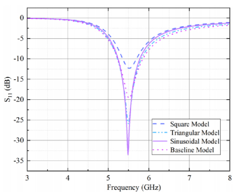
Figure 8: Comparison of the reflection coefficient () for four different topology dipole antennas.
The comparison of the four antenna models’ return loss was performed in the frequency range of 3-8 GHz, with a focus on performance around the center frequency of 5.5 GHz. The four models are: Square Model (dark blue dashed line), Triangular Model (light blue dash-dot line), Sinusoidal Model (purple solid line), and Baseline Model (pink dotted line), as shown in Fig. 8. Overall, the Triangular Model and Sinusoidal Model achieve a better balance between return loss depth and bandwidth. Specifically, the Triangular Model reaches a minimum return loss of -22 dB, with a -10 dB bandwidth of 580 MHz. The Sinusoidal Model further improves the minimum return loss to -31 dB, with a bandwidth of 500 MHz. The Baseline Model, while having the widest bandwidth of 600 MHz, achieves a minimum return loss of only -18.5 dB. The Square Model, with a shallower minimum return loss of -11 dB and the narrowest bandwidth of 350 MHz, shows better suitability for compact designs. The detailed performance parameters for all four antennas are listed in Table 2.
Table 2: Comparison of different antenna structures
| Type | Ant.1 | Ant.2 | Ant.3 | Ant.4 |
| (mm) | 30 | 25 | 25 | 18 |
| Patch_ln (mm) | 22.7 | 20.1 | 20 | 14.7 |
| Size Reduction | N/A | 17.2% | 17.2% | 40% |
| Reflection Coefficient (dB) | -18.5 | -31 | -22 | -12.7 |
| Band Width (MHz) | 600 | 500 | 580 | 350 |
| Gain (dBi) | 1.98 | 2.02 | 1.94 | 1.9 |
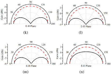
Figure 9: Comparison of gain radiation pattern for four different topology dipole antennas. The red dashed line represents the E-plane, and the black solid line represents the H-plane. (a) Baseline. (b) Sinusoidal. (c) Triangular. (d) Square.
The comparison of the four antenna models’ reflection coefficients () was performed in the frequency range of 3-8 GHz, with a focus on performance around the center frequency of 5.5 GHz. The four models are: Square Model (dark blue dashed line), Triangular Model (light blue dash-dot line), Sinusoidal Model (purple solid line), and Baseline Model (pink dotted line), as shown in Fig. 8. Overall, the Triangular Model and Sinusoidal Model achieve a better balance between the reflection coefficient and bandwidth. Specifically, the Triangular Model reaches a minimum reflection coefficient () of -22 dB, with a -10 dB bandwidth of 580 MHz. The Sinusoidal Model further improves the minimum reflection coefficient () to -31 dB, with a bandwidth of 500 MHz. The Baseline Model, while having the widest bandwidth of 600 MHz, achieves a minimum reflection coefficient () of only -18.5 dB. The Square Model, with a shallower minimum reflection coefficient () of -11 dB and the narrowest bandwidth of 350 MHz, shows better suitability for compact designs. The detailed performance parameters for all four antennas are listed in Table 2.
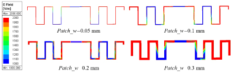
Figure 10: Electric field distribution with different line widths.
To further analyze and compare the performance of the four antennas, their gain radiation patterns are shown in Fig. 9. The gain patterns display the antennas’ radiation performance at a frequency of 5.5 GHz, with the vertical axis representing gain (in dBi). The radiation patterns show symmetry and stability, with the red dashed line representing the E-plane () and the black solid line representing the H-plane (). From the peak gain readings, it is evident that the Square Model antenna does not experience a significant reduction in gain despite its compact size.
The comparison of the four antenna topologies is shown in Table 2. From Table 2, it is clear that, compared to the other models, the Square Model has the smallest size at the 5.5 GHz operating frequency, with its reflection coefficient, bandwidth, and gain all within the normal operating range.
To investigate the effect of patch width on antenna gain, the surface current distribution characteristics of three different line-width antennas were compared. Simulation results show that as the line width increases, the surface current distribution becomes more uniform, and the current density in the radiation region increases significantly. This uniform current distribution reduces the ineffective power loss within the antenna, thereby improving radiation efficiency. Furthermore, the increase in line width expands the current radiation area, enhancing the antenna’s equivalent radiation area, and further improving its directivity and gain. A detailed comparison of the electric field distributions is shown inFig. 10.
B. Tag design and simulation
The tag design process typically involves the following steps: determining the operating frequency of the tag, selecting the diode model to be used, establishing the diode port impedance, designing the antenna topology, selecting the dielectric substrate material, and designing the matching circuit between the diode and the tag antenna. Since tag operations often work near the X-band frequency range [35], this study uses 5.5 GHz as the fundamental frequency of the tag. In section II, harmonic simulations and calculations show that the SMS-7630 diode exhibits low CL, making it the chosen nonlinear component for this work. In section III.A, with the objectives of minimizing size while maintaining high antenna radiation gain, the performance of different folded antenna topologies is analyzed through simulations, leading to the selection of the Square Model as the tag antenna topology. Additionally, simulations of current distribution reveal that increasing the width of the antenna’s radiation patch enhances the gain.
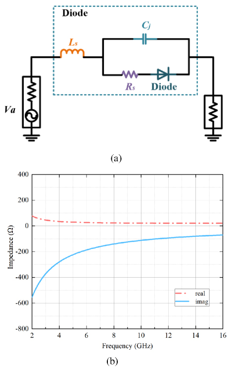
Figure 11: Diode impedance simulation: (a) Diode model simulation. (b) The impedance values of the SMS-7630 Schottky diode.
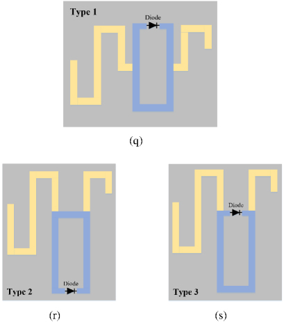
Figure 12: Three parallel inductive matching circuit methods. (a) Center. (b) Down. (c) Top.
The determination of the diode impedance is critical, as it directly affects harmonic conversion efficiency and the design of the matching circuit. Figure 11 shows the simulated impedance variations of the SMS-7630 diode at different frequencies. At the fundamental frequency of 5.5 GHz, the diode impedance is ; at the harmonic frequency of 11 GHz, the impedance is . By adjusting the antenna structure and introducing a matching circuit, conjugate matching between the tag antenna and the diode can be achieved. Furthermore, as shown in Table 3, PI stands out as the ideal material for lightweight tag design among common dielectric substrates.
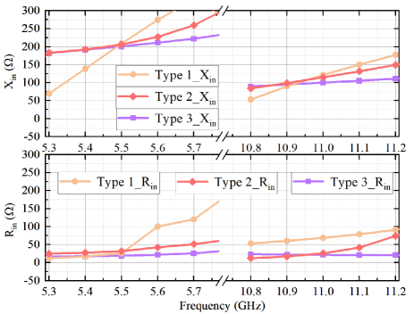
Figure 13: The impedance plots of three parallel inductance configurations.
Table 3: Comparison of different materials
| Material | FR4 | PI | Rogers RO4350B | Teflon ZYF300CA |
| 2.2 | 3.3 | 3.48 | 3.0 | |
| Density () | 1.8 | 1.37 | 1.86 | 2.27 |
| Mass (g) | 1.8 | 1.37 | 1.86 | 2.27 |
Common dielectric substrate materials are listed in Table 3. For example, PI has a density of 1.37 , FR4 has a density of 2.23 , Teflon ZYF300CA has a density of 2.27 , and Rogers RO4350B has a density of 1.86 . Based on the mass-density formula , the mass of PI is the lightest at 1.37 g. Furthermore, the PI substrate is flexible, making it ideal for lightweight tag designs. Therefore, PI material (dielectric constant 3.3) is selected to support the low-mass design of the tag.
Matching circuits are crucial components in the tag design. Figure 12 illustrates three types of matching circuits. In the diagram, the gray regions represent the dielectric substrate, the yellow areas denote the radiation patches, and the blue sections correspond to the diode’s parallel inductive matching circuits.
Matching circuits are critical components in tag design. To ensure stable tag operation, it is essential to choose a matching circuit with impedance stability near the operating frequency range. Figure 12 compares three types of parallel inductive matching circuits. In the illustration, gray regions represent the dielectric substrate, yellow areas denote the radiation patches, and blue sections correspond to the parallel inductive matching circuits of the diode.
Figure 13 illustrates the impedance simulation results for three types of matching circuits, offering a comparative analysis of their performance. The diagram is divided into two segments: the lower segment shows the real part of the impedance (), while the upper segment represents the imaginary part (). The frequency ranges under consideration are 5.3–5.7 GHz for the fundamental frequency and 10.8–11.2 GHz for the harmonic frequency, with a discontinuity separating these ranges. The orange, red, and purple lines correspond to Type 1, Type 2, and Type 3 matching circuits, respectively.
The impedance simulation reveals that the Type 1 matching circuit experiences the largest variation in impedance, indicating potential instability across the operating frequencies. While the impedance variations for Type 2 and Type 3 are relatively close, the impedance of Type 3 demonstrates greater stability, particularly at the harmonic frequencies, with a smaller rate of change compared to Type 2. This stability is critical for ensuring efficient signal processing and minimizing mismatch losses, especially in nonlinear circuits like those involving harmonic tags.
Given these observations, Type 3 is deemed the most appropriate choice for the tag’s matching circuit, as it offers a superior balance of impedance stability and performance over the required frequency ranges.
The previous analysis concluded that increasing the line width of the microstrip dipole helps improve the current distribution of the tag antenna. To further enhance the performance of the square antenna, the impact of widening the line width was examined. A wider line width increases the current distribution, which boosts the gain and, in turn, improves the radiation efficiency. Additionally, a wider line width optimizes the current distribution on the antenna surface, thereby minimizing losses caused by current concentration. Therefore, increasing the line width not only improves the antenna gain but also optimizes its overall radiation performance. The relationship between tag gain and radiation patch width is shown in Fig. 14.
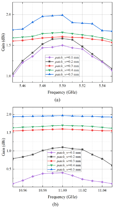
Figure 14: Comparison of gain for different line widths. (a) Fundamental frequency (b) Harmonic frequency.
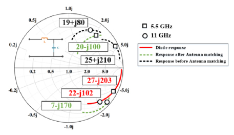
Figure 15: Smith chart matching.
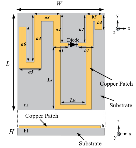
Figure 16: Schematic diagram of the topology structure of the tag in this work.
The impedance matching between the tag antenna and the diode was analyzed using simulation software, and the results are shown in the Smith chart in Fig. 15. The solid red curve represents the impedance variation of the diode, while the dashed green and black curves represent the impedance variations of the tag antenna before and after matching, respectively. The square markers correspond to the fundamental frequency of 5.5 GHz, and the circular markers correspond to the harmonic frequency of 11 GHz. By introducing a series inductor into the tag antenna and a parallel capacitor into the diode, conjugate matching between the tag antenna and the diode was achieved at both the fundamental and harmonic frequencies.
The final tag structure is shown in Fig. 16, which illustrates the geometric configuration of the tag, including the radiation patches and the dielectric substrate. The diode is soldered between the radiation patches. The yellow regions represent copper radiation patches, labeled to and to . The patches labeled with lengths and act as inductive loops, facilitating impedance matching between the antenna and the diode. The gray region indicates the dielectric substrate(PI, dielectric constant 3.3). Detailed parameters of the tag antenna are listed in Table 4.
Table 4: Tag structure parameters
| Parameter | Values | Parameter | Values |
| Frequency | 5.5/11 GHz | 0.11 mm | |
| 14 mm | 0.035 mm | ||
| 7.4 mm | to | 14.8 mm | |
| 2.8 mm | to | 6.3 mm | |
| 8 mm | Substrate | PI | |
| Diode Length | 1.2 mm | Diode Type | SMS-7630 |
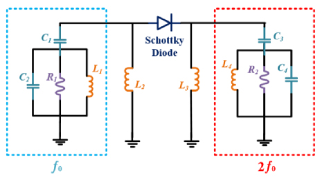
Figure 17: Equivalent circuit model of this work.
FEM simulations are commonly used in antenna design to analyze electromagnetic field distribution, radiation characteristics, and impedance matching. These simulations are crucial for understanding the physical characteristics of the antenna and optimizing its design. However, in tag design, it is also necessary to analyze the equivalent circuit model of the antenna because the tag antenna is typically a component of the tag system. In harmonic radar detection experiments, evaluating the overall performance of the tag—including the diode and the antenna—is more important than solely focusing on the antenna’s electromagnetic properties. By representing the tag antenna and diode as an equivalent circuit model, the tag’s performance can be assessed more intuitively. Therefore, equivalent circuit model simulations were conducted alongside FEM simulations, as shown in Fig. 17.
The simulation results indicate the presence of resonant frequencies at both the fundamental and harmonic frequencies, as shown in Fig. 18, confirming the tag’s effective operation. The FEM simulation results show that the reflection coefficient () is less than -10 dB near 5.5 GHz and 11 GHz, indicating high radiation efficiency, maximizing energy transmission, and improving the tag’s overall efficiency.
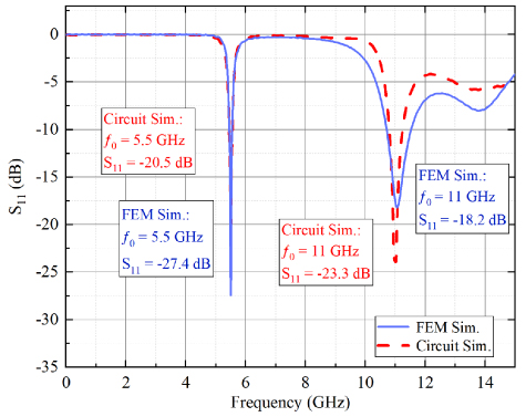
Figure 18: Simulated S-parameters of this work.
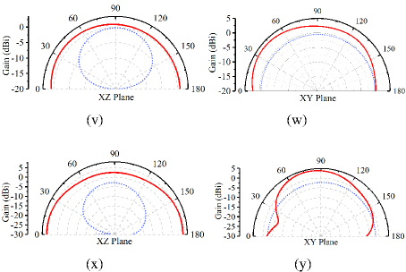
Figure 19: The normalized radiation patterns of the tag at (a), (b) 5.5 GHz and (c), (d) 11 GHz frequencies are shown for the XZ and XY planes.The blue dashed line represents the wire tag, while the red solid line represents this work.
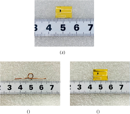
Figure 20: Fabricated tags. (a) Unmodified tag. (b) Wire tag. (c) This work.
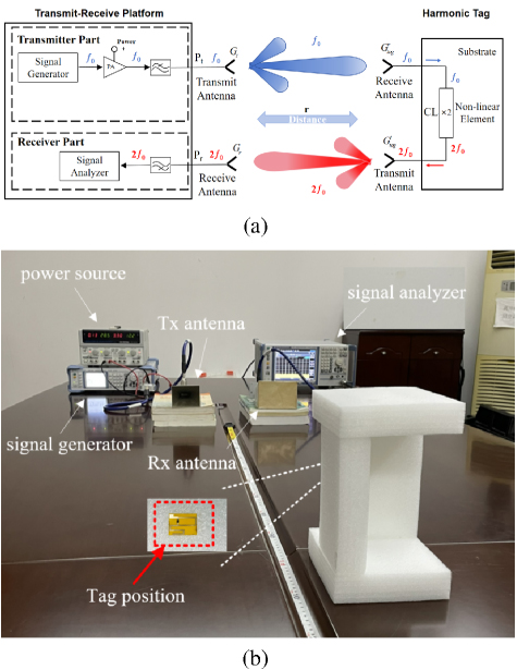
Figure 21: The harmonic experimental testing system for the two types of tags. (a) Indoor harmonic platform test schematic. (b) The measurement setup indoors.
To directly compare the performance of the designed tag, existing tags [15] are reproduced through simulation and fabrication at the same operating frequency for testing. Figure 19 shows the radiation patterns of two tags at the fundamental frequency of 5.5 GHz and the harmonic frequency of 11 GHz. The results indicate that both tags exhibit omnidirectional radiation in the XZ and XY planes. However, the linear tag shows directional deviations in the XZ plane at both frequencies, leading to uneven radiation and limiting the coverage area of the harmonic radar. In contrast, the tag designed in this study demonstrates stronger and more uniform radiation characteristics in its radiation patterns, outperforming the linear tag.
IV. PERFORMANCE MEASUREMENT AND DISCUSSION
Figure 20 presents images of the fabricated tags. The schematic diagram of the indoor testing platform is shown in Fig. 21 (a). During indoor experiments, a signal source emitted the base frequency signal, and a signal analyzer received the harmonic signals generated by the tags. The performance of each tag was assessed based on the displayed received signal power. Stronger signal power indicated superior performance, while weaker signals indicated poorer performance. To assess this work’s performance in simulated real-world conditions, outdoor tests were conducted with harmonic radar in a realistic radio propagation environment. The schematic diagram of the outdoor testing platform is provided in Fig. 23 (a). The harmonic radar receives the echo (harmonic) signals and measures the radar range Doppler. Specific procedures for indoor and outdoor experiments are detailed in sections IV.A and IV.B, respectively.
A. Indoor harmonic system platform testing
Figure 21 (b) illustrates the measurement setup of the indoor testing platform. The tag is affixed to a movable foam material, and the experimental distance is calibrated using a measuring tape. At the transmitting end, the platform consists primarily of a signal generator and a transmitting antenna, while the receiving end includes a signal analyzer and a receiving antenna. To mitigate harmonic interference from the transmitting end, a low-pass filter is placed between the transmitting antenna and the signal generator. Additionally, a power amplifier (PA) is inserted between the signal generator and the low-pass filter to boost transmission power. Table 5 provides the parameters of the harmonic system platform depicted in Fig. 21.
Based on the Friis transmission equation [39], theoretical link budget analysis is conducted to obtain the received power of the signal analyzer:
| (21) |
| (22) |
Table 5: Transceiver link parameters
| Parameter | Value |
| Transmitter power | 11 dBm |
| Tx antenna gain () | 19 dBi |
| Transponder gain () | 1.9 dBi |
| Harmonic CL | 33.8 dB(@-30dBm) |
| Transponder gain (2) | 1.5 dBi |
| Rx antenna gain (2) | 17 dBi |
Table 6: Definition of formula parameters
| Parameter | Definition |
| Receiving power of the instrument | |
| Transmitting power of the instrument | |
| Transmitting antenna gain | |
| Receiving antenna gain | |
| Transmitting antenna gain of the tag | |
| Receiving antenna gain of the tag | |
| Transmission loss | |
| Frequency doubling circuit CL | |
| System circuit loss | |
| Tag conversion gain | |
| Polarization loss |
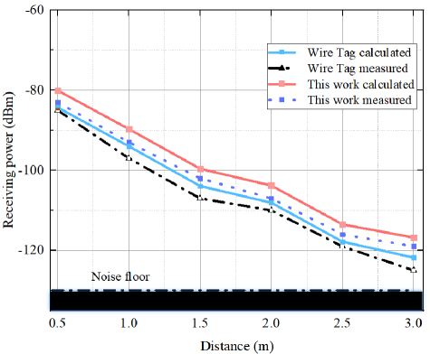
Figure 22: The relationship between tag measurement distance and received power.
According to equation (22), represents the tag’s conversion gain, which indicates the tag’s influence on the system’s received power. It is evident that as the tag gain increases and CL decreases, the tag’s conversion gain increases, leading to stronger tag performance. Definitions of other parameters are provided in Table 6.
Considering the effect of the Fresnel zone on antenna and tag radiation in propagation experiments, the measurement distance needs to be greater than 2*/, where is the maximum linear dimension of the antenna. Therefore, a test distance starting from 0.5 m and totaling 3 m is planned, with measurements taken every 0.5 m. From Fig. 22, it can be seen that the simulation and measurement results of this work are generally consistent, with the difference between them caused by fabrication and soldering tolerances. The unmodified tag’s signal could not be detected at any distance. At a 3-meter range, the wire tag’s reflected signal power measured -123.8 dBm, while our proposed tag achieved -118.3 dBm. Under identical test conditions, our tag demonstrates superior performance compared to both the wire tag and unmodified tag.
Additionally, under the same operating frequency of 5.5 GHz, the wire tag has dimensions of 30 × 5 mm2, with a gain of 0.7 dBi at the fundamental frequency and -1.6 dBi at the harmonic frequency. Its tag conversion gain () is -31.3 dB; this work has more compact dimensions of 12 × 8.4 mm2, with a gain of 1.9 dBi at the fundamental frequency and 1.5 dBi at the harmonic frequency, and a tag conversion gain () of -30.4 dB. This study achieves a reduction in tag size, an increase in gain, and consequently, an enhancement in echo power under the same operating frequency as existing tags. The experimental results conclusively demonstrate that the proposed tag design exhibits superior performance and enhanced functionality compared to conventional counterparts. Furthermore, these findings validate the effectiveness of the modified reflection coefficients () calculation methodology.
To gain a deeper understanding of the transponder’s performance under varying incident power densities, we employed a frequency-sweeping method to plot the relationship between received power and transmitted power, as illustrated in Fig. 23. In this figure, we represent the simulated and measured harmonic conversion losses with purple and red curves, respectively, corresponding to the right y-axis. Additionally, we depict the simulated and measured received power with pink and black curves, which align with the left y-axis, facilitating a straightforward comparison between the theoretical model and experimental data.
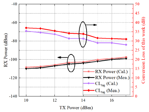
Figure 23: Measured and simulated received power and CL versus the transmitted power.
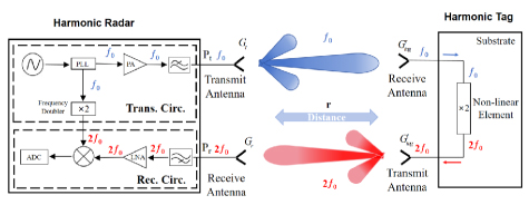
Figure 24: Harmonic radar schematic diagram.
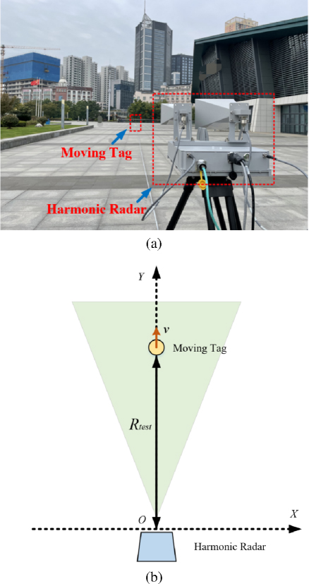
Figure 25: Harmonic radar detection experiment. (a) Harmonic radar test experimental scene. (b) Experimental scene diagram.
During the measurement, the signal generator output power was set from 10 to 17 dBm, while the noise floor of the spectrum analyzer was –125 dBm. To ensure data reliability, the transmit power was reduced in 1 dB steps. The measured results closely follow the trend of the simulated curve, with any deviations mainly caused by fabrication and soldering tolerances.
B. Outdoor harmonic radar testing
The results of the indoor experiments demonstrate the superiority of this approach. To evaluate its performance in real-world conditions, harmonic radar was employed in an outdoor setting to detect moving tags. The radar system transmits a fundamental frequency signal at 5.5 GHz and receives a harmonic frequency signal at 11 GHz. The precise system parameters are detailed in Table 7.
Table 7: Harmonic radar system parameters
| Parameter | Value |
| Frequency | 5.5/11.0 GHz |
| Waveform | Sawtooth FMCW |
| Transmitting Power | 10 W(40 dBm) |
| Valid Bandwidth | 50/100 MHz |
| Chirp Period | 500 s |
| Gain of TX Antenna | 19.13 dBi@5.5 GHz |
| Gain of Rx Antenna | 21.27dBi@11.0 GHz |
Outdoor field experiments were conducted using a harmonic radar system in an open area to validate the performance of the proposed harmonic tag.The harmonic radar consists of a transmit path and a receive path, as illustrated in Fig. 24.
In the transmit path, a high-precision oscillator and a phase-locked loop (PLL) are employed to generate a stable 5.5 GHz fundamental signal with low phase noise. The signal is amplified by a PA, filtered to suppress out-of-band noise, and transmitted through a directional antenna to ensure efficient radiation toward the target.The receive path is designed to capture the second harmonic response generated by the nonlinear behavior of the tag. The received 11 GHz signal is filtered, amplified by a low-noise amplifier (LNA), and mixed with a locally generated 11 GHz signal produced by a frequency doubler driven by the same PLL source. After mixing, an intermediate frequency (IF) signal is obtained, which is subsequently digitized by an analog-to-digital converter (ADC) for further processing, including target detection and localization analysis.The experimental setup is shown in Fig. 25 (a), where two squares indicate the positions of the harmonic radar and the moving tag. The harmonic radar is located at the origin, with the y-axis aligned with the radar’s main lobe direction and the x-axis perpendicular to it, as illustrated in Fig. 25 (b).
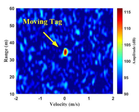
Figure 26: Harmonic radar receiving tag echo power.
Table 8: Comparison between this paper and previous related works
| Ref. | [20] | [21] | [40] | Wire tag | This work | ||||
| Application | Track Insect | Track Insect | Monitor Wall | Track Insect | Track Insect | ||||
| Type | Passive | Passive | Passive | Passive | Passive | ||||
| Polarization | LP | LP | LP | LP | LP | ||||
| Op. freq. (GHz) | 9.41 | &18.8 | 5.88 | 1.2 | &2.4 | 5.5 | &11 | 5.5 | &11 |
| Substr. | Copper | Rogers | Paper | Copper | PI | ||||
| Area/2 | 0.53×0.53 | 0.53×0.53 | 0.3×0.26 | 0.53×0.53 | 0.25×0.15 | ||||
| Gain(dBi) | @;@ | \ |
\ |
3.3;3 | -0.7;-1.6 | 1.9;1.5 | |||
| (dBm) | @-30dBm | \ |
\ |
-37 | -33.8 | -33.8 | |||
| (dBm) | @-30dBm | \ |
\ |
-30.7 | -36.1 | -30.4 | |||
| Mass | 12mg | 6mg | 3g | 10mg | 5mg |
Figure 25 (b) depicts the positional information: the blue area denotes the location of the harmonic radar, the green area delineates its radiation zone, and the yellow area signifies the mobile tag. Throughout the experiment, the tag travels along the positive y-axis direction, where denotes the distance between the tag and the harmonic radar. We can evaluate the performance of the tag in the experiment through the distance Doppler of the harmonic radar.
Figure 26 depicts the distance Doppler information of the tag during its motion. The figure reveals that in the collaborative experiments between the tag and the harmonic radar in this study, there exists robust signal return strength characterized by stable and noise-free signals. Notably, even at a distance of 35 m, the harmonic radar can still capture strong echo signals, thus showcasing the tag’s high performance and its applicability to insect exploration experiments in intricate environments. A comparison between this paper and other state-of-the art works is listed in Table 8. They are all fully passive harmonic transponders. Our proposed harmonic tag not only achieves the smallest size and lightest weight, but also maintains strong signal strength. This makes it particularly advantageous in size- and weight-sensitive applications, such as tracking small organisms (e.g., insects) and environmental monitoring, where the tag’s dimensions, weight, and signal strength are all critical to system performance. By employing an innovative antenna structure and highly efficient nonlinear component matching techniques, we have significantly reduced the overall size and weight of the tag while preserving excellent radiation characteristics and signal conversion efficiency. This optimized design ensures the tag’s adaptability in real-world applications, minimizes interference with the movement of tracked subjects, and greatly enhances its reliability and stability.
V. CONCLUSION
The main contribution of this paper lies in the theoretical analysis of the harmonic generation mechanism and device selection for nonlinear components, the correction of the harmonic tag echo loss calculation formula, and the design of a miniaturized, low-mass insect tag without compromising signal strength. In this study, the fundamental and harmonic frequencies achieved gains of 1.9 dBi and 1.5 dBi, respectively, both of which surpass those reported in previous research. Furthermore, the performance of the tag has been thoroughly validated through established experimental platforms. In an indoor test environment, we used a signal generator emitting 11dBm of power, with echo power measured at -118.3 dBm at a distance of 3 meters and a conversion gain of -30.4 dB, confirming the superiority of our method. Additionally, outdoor tests using harmonic radar also showed strong echo signals. This innovative method contributes to solving the harmonic radar detection and tracking problem by reducing losses, minimizing size and weight, and enhancing the echo signal strength, all of which demonstrate higher performance compared to previous studies. Future work will focus on investigating the adaptability of the tag for insects.
REFERENCES
[1] M. M. Sheikh, “Analysis of reader orientation on detection performance of Hilbert curve-based fractal chipless RFID tags,” Applied Computational Electromagnetics Society (ACES) Journal, vol. 39, no. 6, pp. 490-504, 2024.
[2] L. Zhang, A. Poddar, U. Rohde, and M. Tong, “A novel reconfigurable chipless RFID tag based on notch filter,” Applied Computational Electromagnetics Society (ACES) Journal, vol. 39, no. 9, pp. 801-813, 2024.
[3] C. Chen and Q. Feng, “A compact broadband circularly polarized slot antenna for universal UHF RFID reader and GPS,” Applied Computational Electromagnetics Society (ACES) Journal, vol. 36, no. 5, pp. 589-595, 2021.
[4] R. Ma and Q. Feng, “Broadband CPW-fed circularly polarized square slot antenna for universal UHF RFID handheld reader,” Applied Computational Electromagnetics Society (ACES) Journal, vol. 36, no. 6, pp. 747-754, 2021.
[5] M. N. Zaqumi, J. Yousaf, M. Zarouan, M. A. Hussaini, and H. Rmili, “Passive fractal chipless RFID tags based on cellular automata for security applications,” Applied Computational Electromagnetics Society (ACES) Journal, vol. 36, no. 5, pp. 559-567, 2021.
[6] J. Shefer and R. J. Klensch, “Harmonic radar helps autos avoid collisions,” IEEE Spectr., vol. 10, no. 5, pp. 38-45, 1973.
[7] K. Grasegger, G. Strapazzon, E. Procter, H. Brugger, and I. Soteras, “Avalanche survival after rescue with the RECCO rescue system: A case report,” Wilderness Environ. Med., vol. 27, no. 2, pp. 282-286, 2016.
[8] B. Kubina, J. Romeu, C. Mandel, M. Schüßler, and R. Jakoby, “Design of a quasi-chipless harmonic radar sensor for ambient temperature sensing,” in SENSORS, Valencia, Spain, pp. 1567-1570,2014.
[9] A. Singh and V. M. Lubecke, “Respiratory monitoring and clutter rejection using a CW doppler radar with passive RF tags,” IEEE Sens. J., vol. 12, no. 3, pp. 558-565, 2012.
[10] L. Zhu, H. Huang, M. M.-C. Cheng, and P.-Y. Chen, “Compact, flexible harmonic transponder sensor with multiplexed sensing capabilities for rapid, contactless microfluidic diagnosis,” IEEE Trans. Microw. Theory Techn., vol. 68, no. 11, pp. 4846-4854, 2020.
[11] G. J. Mazzaro, A. F. Martone, and D. M. McNamara, “Detection of RF electronics by multitone harmonic radar,” IEEE Trans. Aerosp. Electron. Syst., vol. 50, no. 1, pp. 477-490, 2014.
[12] V. G. Yadav, L. Zeng, and C. Li, “Circular polarized antennas with harmonic radar: Passive nonlinear tag localization,” IEEE Journal of Selected Areas in Sensors, vol. 1, pp. 9-19, 2024.
[13] D. Mascanzoni and H. Wallin, “The harmonic radar: A new method of tracing insects in the field,” Ecol. Entomol., vol. 11, no. 4, pp. 387-390, 1986.
[14] R. Brazee, E. Miller, M. Reding, M. Klein, B. Nudd, and H. Zhu, “A transponder for harmonic radar tracking of the black vine weevil in behavioral research,” Trans. ASAE, vol. 48, no. 2, pp. 831-838, 2005.
[15] B. Colpitts and G. Boiteau, “Harmonic radar transceiver design: Miniature tags for insect tracking,” IEEE Trans. Antennas Propag., vol. 52, no. 11, pp. 2825-2832, 2004.
[16] N. Tahir and G. Brooker, “Recent developments and recommendations for improving harmonic radar tracking systems,” in Proceedings of the 5th European Conference on Antennas and Propagation (EUCAP), pp. 1531-1535, 2011.
[17] R. Maggiora, M. Saccani, D. Milanesio, and M. Porporato, “An innovative harmonic radar to track flying insects: The case of Vespa velutina,” Sci. Rep., vol. 9, no. 1, p. 11964, 2019.
[18] J. Riley and A. Smith, “Design considerations for an harmonic radar to investigate the flight of insects at low altitude,” Comput. Electron. Agric., vol. 35, no. 2-3, pp. 151-169, 2002.
[19] E. A. Capaldi, A. D. Smith, J. L. Osborne, S. E. Fahrbach, S. M. Farris, D. R. Reynolds, and J. R. Riley, “Ontogeny of orientation flight in the honeybee revealed by harmonic radar,” Nature, vol. 403, no. 6769, pp. 537-540, 2000.
[20] D. Milanesio, M. Saccani, R. Maggiora, D. Laurino, and M. Porporato, “Design of an harmonic radar for the tracking of the A sian yellow-legged hornet,” Ecol. Evol., vol. 6, no. 7, pp. 2170-2178, 2016.
[21] H. Zhu, D. Psychoudakis, R. Brazee, H. Thistle, and J. Volakis, “Capability of patch antennas in a portable harmonic radar system to track insects,” Transactions of the ASABE, vol. 54, no. 1, pp. 355-362, 2011.
[22] A. Lavrenko, B. Litchfield, G. Woodward, and S. Pawson, “Design and evaluation of a compact harmonic transponder for insect tracking,” IEEE Microw. Wirel. Compon. Lett., vol. 30, no. 4, pp. 445-448, 2020.
[23] J. Kiriazi, J. Nakakura, K. Hall, N. Hafner, and V. Lubecke, “Low profile harmonic radar transponder for tracking small endangered species,” in 2007 29th Annual International Conference of the IEEE Engineering in Medicine and Biology Society, pp. 2338-2341, 2007.
[24] Z.-M. Tsai, P.-H. Jau, N.-C. Kuo, J.-C. Kao, K.-Y. Lin, F.-R. Chang, E.-C. Yang, and H. Wang, “A high-range-accuracy and high-sensitivity harmonic radar using pulse pseudorandom code for bee searching,” IEEE Trans. Microw. Theory Techn., vol. 61, no. 1, pp. 666-675, 2012.
[25] N. Tahir and G. Brooker, “Toward the development of millimeter wave harmonic sensors for tracking small insects,” IEEE Sens. J., vol. 15, no. 10, pp. 5669-5676, 2015.
[26] V. Palazzi, F. Alimenti, M. Virili, C. Mariotti, G. Orecchini, P. Mezzanotte, and L. Roselli, “A novel compact harmonic RFID sensor in paper substrate based on a variable attenuator and nested antennas,” in 2016 IEEE MTT-S International Microwave Symposium (IMS), pp. 1-4, 2016.
[27] M. I. M. Ghazali, S. Karuppuswami, and P. Chahal, “Embedded passive RF tags towards intrinsically locatable buried plastic materials,” in 2016 IEEE 66th Electronic Components and Technology Conference (ECTC), pp. 2575-2580, 2016.
[28] S. Mondal and P. Chahal, “A passive harmonic RFID tag and interrogator development,” IEEE J. Radio Freq. Identif., vol. 3, no. 2, pp. 98-107,2019.
[29] F. Yu, K. G. Lyon, and E. C. Kan, “A novel passive RFID transponder using harmonic generation of nonlinear transmission lines,” IEEE Trans. Microw. Theory Techn., vol. 58, no. 12, pp. 4121-4127, 2010.
[30] H. Wang, A. Hsu, K. K. Kim, J. Kong, and T. Palacios, “Gigahertz ambipolar frequency multiplier based on CVD graphene,” in 2010 International Electron Devices Meeting, pp. 23.6.1-23.6.4,2010.
[31] T. Song, H.-S. Oh, J. Yang, E. Yoon, and S. Hong, “A 2.4-GHz sub-mW frequency source with current-reused frequency multiplier,” in IEEE Radio Frequency Integrated Circuits (RFIC) Symposium, 2006, San Francisco, CA, USA, p. 4,2006.
[32] C.-C. Wang, Y.-L. Tseng, H.-C. She, and R. Hu, “A 1.2 GHz programmable DLL-based frequency multiplier for wireless applications,” IEEE Trans. Very Large Scale Integr. (VLSI) Syst., vol. 12, no. 12, pp. 1377-1381, 2004.
[33] S. Mondal, D. Kumar, and P. Chahal, “Recent advances and applications of passive harmonic RFID systems: A review,” Micromachines, vol. 12, no. 4, p. 420, 2021.
[34] R. Ludwig and G. Bogdanov, RF Circuit Design: Theory and Applications, 2nd ed. Noida: Pearson Education India, 2008.
[35] J. Zhang, S. D. Joseph, Y. Huang, and J. Zhou, “Compact single-port harmonic transponder for backscattering communications and energy harvesting applications,” IEEE Transactions on Microwave Theory and Techniques, vol. 71, no. 7, pp. 3136-3143, 2023.
[36] X. Gu, N. N. Srinaga, L. Guo, S. Hemour, and K. Wu, “Diplexer-based fully passive harmonic transponder for sub-6-GHz 5G-compatible IoT applications,” IEEE Transactions on Microwave Theory and Techniques, vol. 67, no. 5, pp. 1675-1687, 2019.
[37] W. L. Stutzman and G. A. Thiele, Antenna Theory and Design. Hoboken, NJ: John Wiley & Sons, 2012.
[38] A. Kumar and A. Lavrenko, “Compact folded meander-line harmonic tag antenna for insect tracking,” in 2023 17th Eur. Conf. Antennas Propag. (EuCAP), pp. 1-5, 2023.
[39] H. T. Friis, “A note on a simple transmission formula,” Proceedings of the IRE, vol. 34, no. 5, pp. 254-256, 1946.
[40] V. Palazzi, F. Alimenti, P. Mezzanotte, G. Orecchini, and L. Roselli, “Zero-power, long-range, ultra low-cost harmonic wireless sensors for massively distributed monitoring of cracked walls,” in 2017 IEEE MTT-S International Microwave Symposium (IMS), Honolulu, HI, USA, pp. 1335-1338, 2017.
BIOGRAPHIES

Zhan-Fei Su was born in Shandong, China. He received the M.S. degree in electronics and communication engineering from the Xi’an University of Posts and Telecommunications, Xian, China in 2021. He is currently working toward the Ph.D. Degree at the School of Electronic Information, Wuhan University, Wuhan, China. His research interests include antennas designs, nonlinear circuit designs, microwave circuit designs, harmonic transponders and their applications.

Xian-Rong Wanwas born in Hubei, China. He received the B.E. degree from the former Wuhan Technical University of Surveying and Mapping, Wuhan, China, in 1997, and the Ph.D. degree from Wuhan University, Wuhan, in 2005. He is currently a Professor and the Ph.D. Candidate Supervisor with the School of Electronic Information, Wuhan University. In recent years, he has hosted and participated in more than ten national research projects and authored or coauthored more than 80 academic articles. His main research interests include design of new radar system such as passive radar, over-the-horizon radar, and array signal processing.

Jian-Xin Yi received the B.E. degree in electrical and electronic engineering and the Ph.D. degree in radio physics from Wuhan University, Wuhan, China, in 2011 and 2016, respectively. From August 2014 to August 2015, he was a Visiting Ph.D. Student with the University of Calgary, Calgary, AB, Canada. He is currently an Associate Professor with the School of Electronic Information, Wuhan University. His main research interests include radar signal processing, target tracking, and information fusion. Dr. Yi was a recipient of the 2017 Excellent Doctoral Dissertation Award of the Chinese Institute of Electronics. He has been supported by the Post-Doctoral Innovation Talent Support Program of China.

Zi-Ping Gong was born in Hubei, China. He received the B.E. and Ph.D. degrees from Wuhan University, Wuhan, China, in 1999 and 2007, respectively. His main research interests include high frequency (HF) radio wave propagation, antenna theory analysis, and antenna design.

Zi-Yao Wang was born in Hubei, China. He received the B.E. degree in measurement and control technology and instrument in 2020 from Wuhan University, Wuhan, China, where he is currently working toward the Ph.D. degree in electronic science and technology. His research interests include design of harmonic radar system and radar signal processing.
ACES JOURNAL, Vol. 40, No. 7, 661–678
doi: 10.13052/2024.ACES.J.400710
© 2025 River Publishers