An Angularly Stable and Polarization Insensitive Miniaturized Frequency Surface for WiMAX Applications
Ze Wang, Huaxin Zhu, Dongming Guo, Xu Gan, and Xianzheng Lyu
School of Science
Jiangnan University, Wu Xi 214122, China
6231206032@stu.jiangnan.edu.cn, zhuhuaxin1312@163.com, 1422737299@qq.com,
2722309952@qq.com, 2103496771@qq.com
Submitted On: March 7, 2025; Accepted On: May 26, 2025
ABSTRACT
This paper presents a miniaturized, polarization insensitive and angularly stable frequency selective surface (FSS) for WiMAX (3.5 GHz) applications. The proposed FSS structure improves upon conventional curved units by incorporating 45 tilted dipoles with extended lengths to increase the effective electrical size. The proposed FSS is printed on float glass with a dielectric constant of 8. The unit cell dimensions are 0.0620.062 (where is the free space wavelength at the first resonant frequency). It exhibits a bandstop characteristic at 3.5 GHz with a bandwidth of 540 MHz (-10 dB). This FSS demonstrates a stable frequency response under incident angles ranging from 0 to 80 for both horizontal and polarization angles. Furthermore, the proposed structure is further analyzed through the derivation of an equivalent circuit model. Finally, a prototype of adequate size is fabricated to validate the simulation results. Both the simulation and measured results confirm the stable performance of the proposed FSS.
Index Terms: Angular stability, bandstop filters, frequency selective surface (FSS), miniaturization, polarization insensitive.
I. INTRODUCTION
With the ongoing miniaturization trend in wireless communication devices, developing miniaturized frequency selective surfaces (FSS) has become essential to address stringent size limitations in modern system integration. As two-dimensional periodic arrays fabricated on dielectric substrates [1–2], FSS exhibit unique frequency-dependent properties that enable selective control of electromagnetic wave transmission, reflection, and absorption [3–4]. Given these features, FSS is extensively employed in centimeter-wave and millimeter wave domains, serving roles in hybrid antenna radomes, radar cross-section (RCS) reduction, antenna reflectors, absorbers, high impedance surfaces, and electromagnetic shielding [5–9]. However, practical applications are often constrained by limited spatial availability. It becomes challenging to accommodate larger physical components to achieve enhanced FSS performance. Therefore, miniaturizing the FSS offers the potential for more precise performance metrics.
Recent years have witnessed significant progress in the development of miniaturized FSS. Jayanandan and Alex proposed a miniaturized FSS operating at 2.45 GHz, which achieved cell miniaturization and stable polarization response by loading distributed reactive elements such as square patches (SP) and meander lines. However, its miniaturized period only reached 0.120.12 [10]. Li et al. developed a compact FSS employing capacitive, inductive, and resonant-type surface impedance elements that attained a remarkable miniaturization factor of 0.0560.056, though the multilayer configuration increased fabrication complexity and the structure maintained satisfactory resonant stability only within a limited 45 incidence angle range [11]. Vardaxoglou and Alexandridis designed a steady-state FSS with 0.0250.025 miniaturization through combined square and triangular structures, but the asymmetric metallic configuration resulted in poor polarization symmetry. These limitations highlight the pressing need for a miniaturized FSS that combines simplified fabrication with excellent polarization response and wide-angle stability [12].
In this study, we propose a miniaturized FSS with a convoluted structure based on the conventional winding technique, and our proposed FSS has excellent miniaturization characteristics compared to other element designs, with a design size of 0.0620.062. In addition, the working mechanism is investigated by surface current distribution and equivalent circuit. Finally, we fabricate the FSS structure as a prototype. Good reflections were obtained in the WiMAX band, and the agreement between the measured and simulated results was very obvious.
II. MINIATURIZED STRUCTURE AND ITS PERFORMANCE
The evolutionary geometry of the proposed miniaturized unit is depicted in Fig. 1. The first design phase features a cross-shaped dipole unit, while the second phase involves a cross-convoluted unit. A cross-convoluted unit is a commonly used structure for miniaturized frequency selective surfaces [13].
The proposed design evolved from the cross-convoluted unit and is comprised of four symmetrically bent units. This tight packing serves to reduce the resonating dimensions of the FSS while increasing the effective electrical size. Based on the conventional cross-curled unit cell, this work introduces an additional 45 tilted dipole to each horizontal strip dipole. Compared to traditional 90 vertical dipoles, this modified configuration occupies a larger physical footprint while effectively enhancing the electrical size. The compact arrangement contributes to the reduction of the FSS’s resonant dimensions. Furthermore, the 45 inclination optimizes the structural coverage ratio, resulting in additional resonant frequency reduction. Meanwhile, the 90 symmetric unit cell facilitates polarization insensitivity. This FSS is printed on float glass with a thickness of 1.6 mm and a dielectric constant of 8, ensuring a low manufacturing cost. The parameters of the final structure unit are provided in Fig. 1 (d) and Table 1. For ease of visualization, Fig. 1 (e) provides a partial enlarged detail. All simulated structures were realized using the ANSYS High Frequency Structure Simulator (HFSS). The proposed FSS structure was modeled under periodic boundary conditions with Floquet port excitation [14].
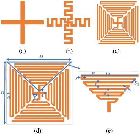
Figure 1: Design evolution of the structure: (a) cross-shaped dipole unit, (b) cross-convoluted unit, (c) final structure unit, (d) proposed FSS unit, and (e) partial enlarged detail.
Table 1: Dimensions and parameters of Fig. 1
| Parameter | D | w | d | g | s |
| Value (mm) | 5.3 | 0.2 | 0.15 | 0.11 | 0.1 |
| Parameter | S | S | p | a | t |
| Value (mm) | 0.55 | 0.35 | 4.65 | 0.05 | 0.1 |
To systematically investigate the frequency response evolution of the FSS structure, our analysis begins with fundamental unit cell configurations: the basic cross-shaped dipole and its convoluted counterpart. The periodicity of this cross-shaped dipole unit and cross-convoluted unit aligns unit with that of the final structure unit. Figure 2 presents the transmission curves for three designs. As observed in Fig. 2, with increasing coiling, the resonant frequency of the FSS structure decreased dramatically from 13.3 GHz to 3.5 GHz, representing a 74% reduction. Likewise, bandwidth (-10 dB) dropped from 2.99 GHz to 0.54 GHz, a decrease of 79%, but this bandwidth perfectly covers WiMAX (3.5 GHz). Hence, from our observations, we discerned that, as the degree of coiling increases, both the resonant frequency and the resonant bandwidth decrease. The decline in resonant frequency can be elucidated using in which L and C represent the equivalent inductance and capacitance, respectively. By amplifying the equivalent inductance and capacitance, the resonant frequency can be reduced. The equivalent inductance, L, is related to the structure’s length, while the equivalent capacitance, C, is associated with the width between structures [15]. The transition from the cross-shaped dipole unit to the final structure unit is marked by an increase in the structural perimeter and a reduction in the inter row spacing, leading to an observed decrease in the resonant frequency. The bandwidth of a bandstop FSS is associated with the ratio of the FSS’s equivalent capacitance to its equivalent inductance (BW) [16]. From the cross-shaped dipole unit to the final structure unit, the change in the structural perimeter is more pronounced than the interspace alteration, resulting in the observed bandwidth reduction.
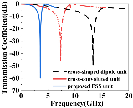
Figure 2: Different structure responses.
Moving forward, we now discuss the impact of varying geometric parameters on the proposed FSS. Figure 3 (a) showcases the effect of line variations on the FSS. As evident from Fig. 3 (a), when parameter d increases from 0.05 mm to 0.2 mm, the resonant frequency of the FSS rises with the widening of the line width, moving from 3.2 GHz to 3.8 GHz. This phenomenon is primarily attributed to the reduction in the corresponding capacitance as the line width increases, thereby elevating the resonant frequency. Furthermore, we examined the influence of variations in the relative permittivity of the dielectric substrate on the FSS. From Fig. 3 (b), it can be observed that, as the dielectric constant increases from 7 to 9, the corresponding resonant frequency decreases from 3.64 GHz to 3.42 GHz. This change stems from the inverse relationship between the resonant frequency and permittivity, as depicted in , where in the formula indicates the resonant frequency in a vacuum [17].
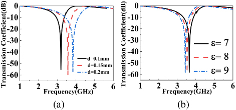
Figure 3: (a) Different line variation responses and (b) different relative permittivity responses.
For practical implementations, the angular stability of miniaturized FSS becomes critical as these structures are routinely exposed to oblique wave incidence spanning 0 to 80 in typical deployment environments [18]. Thus, an FSS that exhibits a stable frequency response under varying angles of incidence is considered a benchmark for quality. Simulations were conducted on the central frequency of the miniaturized FSS using the HFSS software. Figure 4 presents the simulated curves for both TE and TM polarizations at a 0 angle. From Fig. 4, it is evident that the FSS provides consistent responses under both TE and TM polarizations.
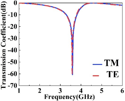
Figure 4: Frequency curves for TE and TM polarization at 0 angle.
Figures 5 (a) and (b) present the simulated curves for both TE and TM polarizations at incidence angle. The results demonstrate that the designed FSS structure exhibits a stable response under both TE and TM polarizations. It is clear from the results that, for TE polarization, the maximum frequency shift for is no more than 0.05 GHz (1.4%). Similarly, for TM polarization, the maximum frequency shift for does not exceed 0.07 GHz (2%).
As the angle of incidence increases, the bandwidth under TE polarization expands, while it narrows under the TM mode. This is attributed to the fact that with the rise in angle of incidence, according to and , is increasing and is decreasing as the angle of incidence increases further [19]. and represent the wave impedance of TE and TM.
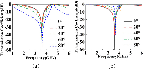
Figure 5: Frequency curves for different angles: (a) 0-80 angle TE polarization, and (b) 0-80 angle TM polarization.
The equivalent current distribution at 3.5 GHz is shown in Fig. 6 (a), where green and blue regions represent high and low current intensities, respectively. At this resonant frequency, the current density is predominantly concentrated on the dipole elements along both lateral edges. Specifically, in the horizontal direction, the current flows sequentially from the leftmost edge dipole to the central cross-shaped unit, and subsequently to the rightmost edge dipole, forming a complete current loop. This distinct current path suggests the establishment of strong current circulation between the lateral dipoles under electromagnetic excitation. In contrast, the vertical current flow between the topmost and bottommost edge dipoles exhibits relatively weaker intensity compared to its horizontal counterpart. Notably, the current magnitude on the lateral dipoles significantly exceeds that on the vertical dipoles. This asymmetric current distribution plays a crucial role in generating the FSS’s stopband characteristics. The enhanced horizontal current response, particularly the strong currents along the lateral edges, contributes substantially to the formation of the stopband effect at specific frequencies. Based on this analysis, the metallic dipoles can be effectively modeled as equivalent inductors (L), while the inter-element gaps are represented as capacitors (C) in the circuit analogy. Figure 6 (b) presents the corresponding equivalent circuit model, which visually demonstrates these electromagnetic characteristics through lumped-element representations [20].
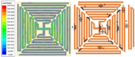
Figure 6: (a) Surface current distribution at 3.5 GHz and (b) FSS circuit schematic.
To validate the full-wave simulation results and further understand the working mechanism of the FSS, we derived an equivalent circuit model of the FSS, as shown in Fig. 7 (a). Here, Z represents the wave impedance of free space, with a value of 377 , and denotes the relative permittivity of the dielectric substrate. The wave impedance of the dielectric substrate, Zsub, can be determined by . Based on the equivalent circuit model in Fig. 7 (a), the impedance at the center frequency of 3.5 GHz is expressed by:
| (1) |
Here, the capacitance C1 represents the gap capacitance between adjacent unit cells, primarily determined by the spacing width and electric field distribution. The inductance L1 corresponds to the structural inductance of the dipole, closely related to its length and current path. Meanwhile, L3 denotes the inductance of the 45 inclined dipole, while L2 and C2 represent the internal inductance of the cross-shaped unit and the gap capacitance between the dipole and the cross-shaped structure, respectively. According to the resonant frequency formula , increasing parameters a or s enhances the coupling area between unit cells and reduces the electric field intensity between metallic structures, thereby increasing the equivalent capacitance C1. Conversely, increasing parameters p, S2, or the edge dipole length extends the current path, leading to higher equivalent inductances L1 and L2, which shifts the resonant frequency toward lower frequencies. The inductance of the 45 tilted dipole, denoted as L3, can be effectively tuned by adjusting parameters d and w. Increasing these parameters reduces the metallic trace inductance, consequently decreasing the equivalent inductance L3. This reduction in L3 shifts the resonant frequency toward higher frequencies.
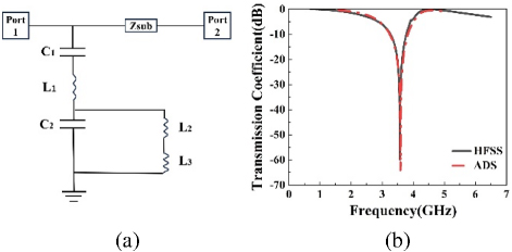
Figure 7: (a) Equivalent circuit of the proposed bandstop FSS structure and (b) ADS software and HFSS software transmission coefficient.
Within the Advanced Design System (ADS), the equivalent circuit model for the FSS was simulated. Based on the equivalent current distribution and the circuit schematic of the FSS, we imported the equivalent circuit structure into the ADS software and derived the values of the superimposed components. To accurately extract the capacitance and inductance values in the equivalent circuit, we employed an optimization-based fitting method that considers transmission zeros and bandwidth characteristics. The inductance (L) and capacitance (C) values were constrained within ranges of 0.01-10 nH and 0.01-10 pF, respectively, for random sampling using ADS software. These parameter ranges were determined through systematic analysis of the FSS’s geometric parameters and electromagnetic properties, ensuring comprehensive coverage of the potential parameter space. During the optimization process, the built-in optimization tools in ADS were employed to perform curve fitting for the equivalent circuit model. The model’s accuracy was evaluated by comparing the S parameters obtained from ADS simulations with HFSS simulation results. The specific optimization strategy consisted of two main steps. First, adjusting the inductance and capacitance values to align the transmission zero and pole of the equivalent circuit model with the HFSS simulation results and, subsequently, further optimizing these values to ensure the bandwidth characteristics matched the HFSS results. Figure 7 (b) illustrates the response of ADS and HFSS, showing that the transfer coefficients of both are in good agreement. In each iteration, the error between the simulated results and HFSS data was calculated. Systematic adjustments of the inductance and capacitance values were made to progressively reduce this error until the iterative error converged below 5%. Through multiple optimization iterations, precise inductance and capacitance values were ultimately obtained, as presented in Table 2.
Table 2: Circuit parameters of FSS
| Parameter | L | L | L | C | C |
| Value (nH/pF) | 1.27 | 1.86 | 0.84 | 0.64 | 0.15 |
III. EXPERIMENTAL RESULTS AND DISCUSSION
The proposed fabricated FSS prototype is shown in Fig. 8 (a), where an array of 1818 cells with a size of 2020 cm was printed on float glass by photolithography process. Figure 8 (b) shows the photograph of the measurement setup. It consists of two horn antennas operating in the 1-18 GHz range, both of which are connected to a FieldFox N9918A handheld vector network analyzer. During the transmission curve measurement, the horn antennas were positioned at a certain distance apart, facing each other. Measurements were taken in a standard indoor environment surrounded by absorber material.
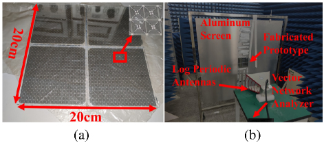
Figure 8: FSS finite prototype and measurement equipment: (a) fabricated prototype and (b) measurement setup.
Based on the measurement results depicted in Fig. 9, a slight deviation in the measured resonant frequency is observed, with an offset of 70 MHz. This deviation has a negligible impact at 3.5 GHz.
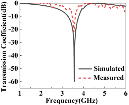
Figure 9: Comparison of simulated curve and measured result.
Concurrently, angular stability tests were performed on the FSS prototype, with results presented in Figs. 10 (a) and (b). When angle is set to 80, the fabricated FSS displays a stable response at the resonant frequency under TE polarization and TM polarization. In the context of TE polarization, angle exhibits a maximum frequency shift of 40 MHz (1.3%), Similarly, for TM polarization, angle reveals a shift of only 60 MHz (2.0%) in the same range.
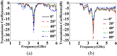
Figure 10: Measured frequency response curve: (a) 0-80 angle TE polarization and (b) 0-80 angle TM polarization.
We fabricated the FSS cells in smaller sizes. Some of the designs in Table 3 have neither high angular stability nor polarization insensitivity, and most of the FSS structures have lower angular stability than our designs. As can be seen in Table 3, the single-layer FSS structures we designed and printed are ultra-miniaturized, highly polarization-insensitive, and angularly stable.
Table 3: Comparison of the proposed FSS structure with previous miniaturized FSS studies
| Ref. | Unit Cell Size (mm) | Periodicity() | Angular Stability | Polarization Insensitive |
| [21] | 11.4 | 0.091 | 80 | YES |
| [22] | 25 | 0.29 | 60 | YES |
| [24] | 9.5 | 0.125 | 45 | YES |
| [25] | 6.25 | 0.05 | 75 | NO |
| This Work | 5.3 | 0.062 | 80 | YES |
IV. CONCLUSION
In this study, we introduce a miniaturized and polarization-stabilized FSS design based on the improvement of a conventional cross-convolutional unit. The improved design has higher polarization stability and smaller cell size than the conventional cross-convolution FSS. The resonant frequency is 3.5 GHz and the suppression bandwidth is 540 MHz (-10 dB), which perfectly covers the WiMAX band (3.5 GHz). In addition, the design has been proven to show a stable frequency response over a range of incidence angles from 0 to 80 for both TE and TM polarization.
ACKNOWLEDGMENT
This work was supported by the National Natural Science Foundation of China (61605067); Open Fund of Key Laboratory of Optical System Advanced Manufacturing Technology, Chinese Academy of Sciences (KLOMT190103).
REFERENCES
[1] B. A. Munk, Frequency Selective Surfaces Theory and Design. New York, NY: Wiley, 2000.
[2] J. Yiannis and C. Vardaxoglou, Frequency Selective Surfaces Analysis and Design. New York, NY: Wiley, 1997.
[3] T. K. Wu, Frequency Selective Surface and Grid Array. New York, NY: Wiley, 1995.
[4] J. C. Vardaxoglou, Frequency Selective Surfaces: Analysis and Design. New York, NY: Wiley, 1997.
[5] A. Malekara, C. Ghobadi, and J. Nourinia, “A frequency selective absorber with anisotropic reflection band for radar cross section reduction,” IEEE Access, vol. 11, pp. 132557-132566, 2023.
[6] A. Ericsson, M. Zhou, S. B. Sørensen, T. Rubæk, M. Riel, and N. J. G. Fonseca, “Modulated frequency-selective doubly curved sub-reflector for a dual-band multiple spot beam communication satellite antenna system,” IEEE Transactions on Antennas and Propagation, vol. 72, pp. 9152-9163, 2024.
[7] Y. Fu, F. Ding, J. Jin, H. Cheng, Y. Yang, X. Zhou, Y. Dai, and H. Yang, “Conformal frequency selective rasorber in S, C, X-band with low backward-scattering,” Opt. Express, vol. 32, pp. 16879-16890, 2024.
[8] M. Li, C. Zhang, X. Yang, D. Zeng, and Z. Yi, “An ultrawideband and wide-angle absorber based on mushroom-type high impedance surface,” IEEE Antennas and Wireless Propagation Letters, vol. 23, pp. 4368-4372, 2024.
[9] Q. Li, Q. Wang, H. Zhang, J.-Q. Hou, and J. Zhao, “A new miniaturized double stop-band frequency selective surface,” Applied Computational Electromagnetics Society (ACES) Journal, vol. 39, pp. 9-16, 2024.
[10] T. Jayanandan and Z. C. Alex, “A miniaturized embedded frequency selective surface-based EMI shield for microwave ovens,” International Journal of Communication Systems, vol. 38, no. 5, 2025.
[11] Z. Li, X. Weng, X. Yi, W. Duan, K. Li, M. Bi, T. Pan, and Y. Lin, “A miniaturized ultrawideband dual-bandpass frequency-selective surface with high selectivity,” IEEE Transactions on Antennas and Propagation, vol. 72, pp. 6510-6519, 2024.
[12] Y. Vardaxoglou and A. A. Alexandridis, “Frequency selective surface with a bistable auxetic geometry,” Electronics Letters, vol. 60, no. 12, 2024.
[13] S. Nan, Z. Hou, L. Guiyuan, and X. Haiyang, “Miniaturized frequency selective surface based on meander lines unit,” Journal of Detection & Control, vol. 32, pp. 87-89, 2010.
[14] A. Chatterjee and S. K. Parui, “Frequency-dependent directive radiation of monopole-dielectric resonator antenna using a conformal frequency selective surface,” IEEE Transactions on Antennas and Propagation, vol. 65, pp. 2233-2239, 2017.
[15] N. Marcuvitz, Waveguide Handbook. Lexington, MA: Boston Technical Publishers, 1964.
[16] P. C. Zhao, Z. Y. Zong, B. Li, W. Wu, and D. G. Fang, “Miniaturized bandstop frequency selective surface based on quasi lumped inductor and capacitor,” Electronics Letters, vol. 53, pp. 642-643, 2017.
[17] M. B. Yan, S. B. Qu, J. F. Wang, J. Q. Zhang, H. Zhou, H. Y. Chen, and L. Zheng, “A miniaturized dual band FSS with stable resonance frequencies of 2.4 GHz/5 GHz for WLAN applications,” IEEE Antennas and Wireless Propagation Letters, vol. 13, pp. 895-898, 2014.
[18] K. Z. Zhang, W. Jiang, J. Y. Ren, and S. X. Gong, “An annular-ring miniaturized stopband frequency selective surface with ultra-large angle of incidence,” Progress in Electromagnetics Research M, vol. 65, pp.19-27, 2010.
[19] P. S. Wei, C. N. Chiu, and T. L. Wu, “Design and analysis of an ultraminiaturized frequency selective surface with two arbitrary stopbands,” IEEE Transactions on Electromagnetic Compatibility, vol. 61, pp. 1447-1456, 2019.
[20] A. B. Varuna, S. Ghosh, and K. V. Srivastava, “A miniaturized element bandpass frequency selective surface using meander line geometry,” Microwave and Optical Technology Letters, vol. 59, pp. 2484-2489, 2017.
[21] D. M. Liu, B. Chen, S. W. Ji, and J.-F. Ruan, “A thin and miniaturized bandpass frequency selective surface with superior angular stability,” Journal of Electromagnetic Waves and Applications, vol. 39, no. 7, pp. 743-753, 2025.
[22] M. Idrees, S. Buzdar, S. Khalid, and M. A. Khalid, “A miniaturized polarization independent frequency selective surface with stepped profile for shielding applications,” Applied Computational Electromagnetics Society (ACES) Journal, vol. 31, pp. 531-536, 2021.
[23] S. Das, A. Rajput, and B. Mukherjee, “A novel FSS-based bandstop filter for TE/TM polarization,” IEEE Letters on Electromagnetic Compatibility Practice and Applications, vol. 6, pp. 11-15, 2024.
[24] L. Murugasamy and R. Sivasamy, “A single layer interdigitated loop elements-based miniaturized frequency selective surface for WLAN shielding,” IEEE Transactions on Consumer Electronics, vol. 70, pp. 617-626, 2024.
[25] Z. U. Abidin, Q. Cao, and G. Shah, “Design of a compact single-layer frequency selective surface with high oblique stability,” IEEE Transactions on Electromagnetic Compatibility, vol. 64, pp. 2060-2066, 2022.
BIOGRAPHIES

Ze Wang was born in Puyang, Henan, China, in 1999. He received the B.S. degree from the Xiamen University of Technology, Xiamen, China, in 2023. Currently, he is focusing on antenna and microwave devices.

Huaxin Zhu received his Ph.D. degree in 2011. Since 2011, he has worked on optical thin film design, preparation and frequency selective surfaces. Currently, he is an Associate Professor in the Jiangnan University, School of Science, China.

Dongming Guo was born in Quanzhou, Fujian, China, in 2000. He received the B.S. degree from the Xiamen University of Technology, Xiamen, China, in 2022. Currently, he is focusing on antenna and microwave devices.

Xu Gan was born in Zaozhuang, Shandong, China, in 2000. He received the B.S. degree from the Xiamen University of Technology, Xiamen, China, in 2024. Currently, he is focusing on antenna and microwave devices.

Xianzheng Lyu was born in Jining, Shandong, China, in 2000. He received the B.S. degree from the Xiamen University of Technology, Xiamen, China, in 2024. Currently, he is focusing on antenna and microwave devices.
ACES JOURNAL, Vol. 40, No. 6, 534–540
doi: 10.13052/2024.ACES.J.400606
© 2025 River Publishers