A Novel GaN Power Amplifier Based on Quasi-Monolithic Microwave Integrated Circuits
Letian Guo1, Shunli Ma1, Hou Yi Ding2, and Mei Song Tong2
1State Key Laboratory of ASIC and System, Fudan University, Shanghai 200438, China
19112020081@fudan.edu.cn, shunlima@fudan.edu.cn
2Department of Electronic Science and Technology Tongji University, Shanghai 201804, China
mstong@tongji.edu.cn
Submitted On: April 07, 2025 Accepted On: August 21, 2025
Abstract
In this paper, we propose a compact quasi-monolithic microwave integrated circuit (MMIC) ultra-wideband gallium nitride (GaN) power amplifier (PA), highlighting its innovative design approach and the associated fabrication techniques aimed at enhancing integration and performance. The discrete transistor is manufactured by a -m GaN high electron mobility transistor (HEMT) process. The input matching network employs a GaAs passive device process for compact and wideband flexible design. The output matching network employs a ceramic technology for high power and low insertion loss design. The discrete transistor is connected to the input and output network with gold bonding wires. The PA exhibited a gain of dB, a saturation power of dBm, and a peak power-added efficiency of .
Keywords: Gallium nitride (GaN), matching network, monolithic microwave integrated circuit (MMIC), power amplifier (PA), ultra-wideband..
1 INTRODUCTION
Broadband power amplifier (PA) monolithic microwave integrated circuits (MMICs) are extensively studied and applied in electronic systems such as electronic countermeasure and multifunction platforms [1, 2, 3, 4]. The key performance metrics, including the output power () and power-added efficiency (PAE), can critically impact the overall effectiveness of these systems [5, 6, 7, 8]. The gallium nitride high electron mobility transistors (GaN HEMTs) on silicon carbide (SiC) substrates can offer notable advantages in radio-frequency (RF) applications, including the high breakdown voltage, superior current handling capability, and elevated power density [9]. Consequently, numerous high-power and high-efficiency GaN-based PAs have been proposed [10, 11]. To enhance their performance, a variety of advanced techniques have been developed, such as stacked field effect transistor (FET) technology [12], reactive filter synthesis, and asymmetric magnetically coupled resonator (MCR) technology [13].
Distributed amplifiers (DAs) have attracted considerable interest due to their excellent return loss and wide bandwidth characteristics [14]. By incorporating the parasitic capacitance of multiple transistors into artificial transmission lines, the DAs can achieve a broadband operation, which can theoretically extend from the zero frequency to the cutoff frequency of the artificial line. Despite these advantages, the DAs still encounter several limitations [15], including low gain [16], poor efficiency [17], large chip area [18], and restricted output power [19]. To address these challenges, reactive matching power amplifiers have been proposed, albeit at the expense of increased design complexity.
In this paper, we propose a novel two-stage GaN PA based on the quasi-MMICs and the analysis, design, and implementation for it with a reactive matching network are presented. The high-pass and low-pass filter matching techniques are employed to achieve effective impedance transformation. Resistors are incorporated into the input-stage matching network to improve the circuit stability and enhance gain flatness across the operating band. Based on the proposed design methodology, the amplifier can operate over the frequency range of 2–6 GHz and deliver an output power () of exceeding W with a PAE ranging from to and an averaged small-signal gain of dB. Simulation and experimental results demonstrate the excellent performance of the proposed PA through a comparison with other PAs available in literature.
2 TRANSISTOR MODELING METHODOLOGY
Transistor modeling is a crucial step in amplifier circuit design optimization, and building accurate transistor models plays a vital role in optimizing circuit performance [20]. There are two transistor modeling methods: linear small-signal [21] and nonlinear large-signal modeling [22]. Linear small-signal modeling extracts linear parameters through the -parameters in each bias state to establish small-signal models. Large-signal modeling extracts nonlinear parameters based on current-voltage (I-V) test data to establish a large-signal model. By integrating and optimizing the extracted linear and nonlinear parameters, a complete model of the transistor that satisfies both S parameters and IV characteristics is established.
The transistor used in this paper is a GaN high electron mobility transistor (HEMT), which is modeled as a small-signal equivalent circuit using the 15 elements field-effect transistor model, with the structure shown in Fig. 1.
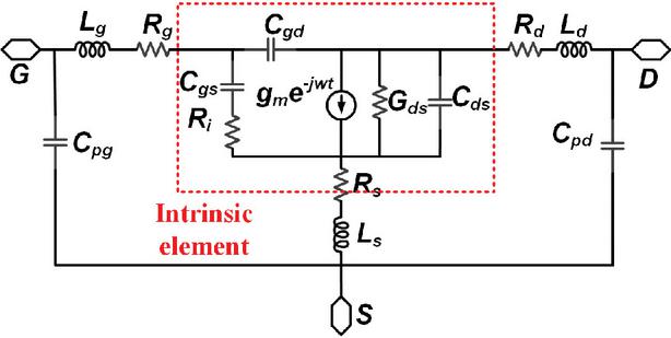
Figure 1 Small-signal equivalent circuit model.
The parasitic capacitance and are extracted by the Dambrine method [23], the parasitic resistance is extracted by the Yang-Long method [24], and the rest of the parasitic parameters are extracted by the ColdFET method [25]. After extracting the parasitic component parameters, the -parameters can be converted to -parameters, and the influence of parasitic components can be removed from the -parameters, i.e., “de-embedding” [26], and the de-embedded -parameters can be converted to -parameters to extract the corresponding parameter values of the intrinsic components. The corresponding equivalent circuits of the intrinsic components are shown in Fig. 2.
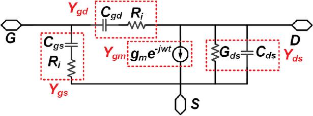
Figure 2 Intrinsic components equivalent circuit.
While the small-signal model is effective for simulating the linear behavior of the device, accurate prediction of nonlinear characteristics, including DC performance and output power behavior, necessitates the use of a large-signal model. The large-signal model of the traditional HEMT is shown in Fig. 3, in which (“IDS” in Fig. 4), , and are three important nonlinear parameters, each of which has a corresponding nonlinear equation.
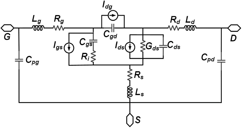
Figure 3 Conventional HEMT large-signal model.
3 AMPLIFIER ARCHITECTURE
Based on the proposed transistor model, a DC bias scan is applied to the transistor and the results are shown in Fig. 4. Considering the output power and efficiency, the base bias voltage is selected to be V and the emitter stage bias voltage is V. At the given bias voltages, the transistor operates in the A and B bias states.
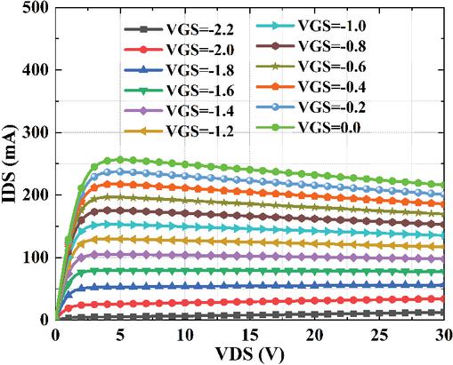
Figure 4 Load-pull results for the model at GHz.
The core is an eight-cell transistor with a single cell which has the gate width m2 , transistor capacitance density of pF/mm, single cell transistor resistance of , the structure shown in Fig. 5. After extracting the impedance parameters of the power tube core model, the output matching circuit design, if the eight cells are matched separately and then combined to the RF output and input ports, the branch will become more, increasing the path loss, and the circuit size is too large. To ensure the simplicity and feasibility of the circuit structure design, in the output matching circuit, the eight cells are divided into two four-cell cores, and then the combined design. In the input matching circuit, the octet is divided into four two-cell cores and then combined.
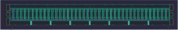
Figure 5 Octal transistor core.
For the passive components in this circuit, the isolation capacitor and the bypass capacitor adopt the general-purpose non-remaining edge type microwave chip capacitor of Tianji Company, whose upper and lower surfaces are gold electrodes, and the middle ceramic dielectric layer is suitable for the bonding and mounting of gold wires and ribbons, and the structure is shown in Fig. 6. A microwave chip capacitor is a single-layer parallel plate capacitor structure, the capacitance depends on the dielectric constant of the dielectric material (K), the thickness of the dielectric material (T) and the size of the electrode .
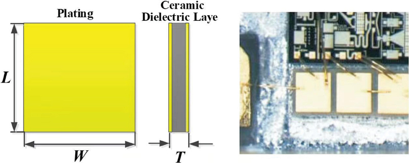
Figure 6 Schematic and physical drawings of general-purpose no-edge-type microwave chip capacitors.
The designed quasi-monolithic PA consists of a tube core, an output matching circuit and an input matching circuit, and the tube core is connected to the matching circuit by a bonding alloy wire. The length of a single gold wire is m and the diameter is m. To realize the high power performance of the amplifier, the output matching circuit is made of alumina substrate, with the dielectric constant of , thickness of m, and copper thickness of m. The input matching circuit is made of a GaAs integrated circuit, with the dielectric constant of , board thickness of m, and metal layer thickness of m.The input matching circuit, the core and the output matching circuit are connected in cascade to obtain the overall structure of the amplifier, which is shown in Fig. 7.
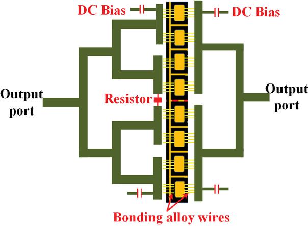
Figure 7 Schematic diagram of quasi-monolithic amplifier structure.
4 OVERALL CIRCUIT DESIGN APPROACH
4.1 Output matching circuit
In power amplifiers, output matching circuits are used to match the optimum output impedance obtained from the transistor by load traction to ohms for maximum output power. The matching circuit is usually realized by using passive devices such as capacitors and inductors as well as microstrip lines, and L-type and -type structures are commonly used for the structure. When designing the output matching circuit, the octal cell is divided into two four-cell cores, and then the combined design is carried out, the structure is shown in Fig. 8.
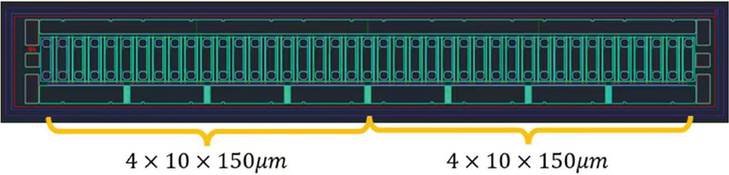
Figure 8 Schematic diagram of an eight-cell transistor core divided into two equal paths.
The parallel equivalent resistance of a single four-cell core is , and the parallel equivalent capacitance is pF/mm10150m4=2.7 pF. The transistor cores are bonded to the output matching circuit by a total of gold wires, and each 4-cell core is connected in parallel using 18 gold wires, with a total of , spaced m single wires measuring m in diameter length and m in diameter. The inductance of a single gold wire is about nF.
The constructed output circuit structure is shown in Fig. 9, and it can be seen that the output matching circuit consists of the parallel RC structure corresponding to the core impedance, the imaginary part compensation network constructed by the bonding alloy wire and the bias feed circuit, the two-order L-type impedance transformation network, and the two-path power synthesis network. Among them, and are equivalent to the optimal output impedance of the four-cell core, is the equivalent inductance introduced by the bonding alloy filament, and the parallel inductor is used to offset the capacitance of the imaginary part of the core impedance, and, at the same time, it plays the role of the drain bias supply. To improve the matching bandwidth, a two-stage low-pass L-type impedance conversion network is used, and the microstrip lines TL1 and TL2 play the roles of impedance conversion and power synthesis.
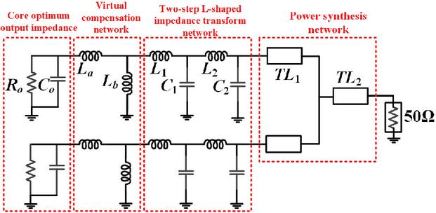
Figure 9 Output matching network circuit.
Based on the above circuit diagram, an output circuit layout is constructed where the inductors , , and are in series microstrip line equivalents and the capacitors and are in parallel open microstrip line equivalents. A ceramic with a dielectric constant of 9.6 and thickness of 380 m is used as the substrate for the output matching circuit, and the dimensions of each microstrip line are shown in Table 1. To accurately process the prepared samples, the high frequency structure simulator (HFSS) is used for modeling and simulation regarding the above simulation layout configuration and data based on the advanced design system (ADS). The HFSS model of the output circuit is shown in Fig. 10. The overall size of the structure is about mm2, and the widths of the microstrip lines are all greater than m, which can satisfy the maximum current and will not be fused due to overheating.
Table 1 Dimensions of microstrip lines in the output matching circuit
| Microstrip Line | Dimension (m) | Microstrip Line | Dimension (m) |
| 3501200 | 9001000 | ||
| 20503700 | 8001700 | ||
| 7001000 | 400700 | ||
| 7001400 | 12002000 |
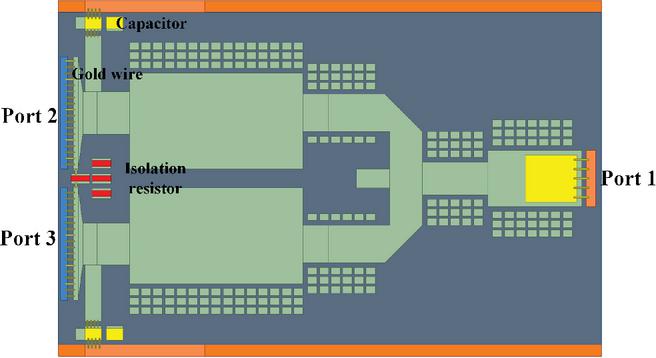
Figure 10 HFSS modeling of output circuits.
The overall simulation results of the output matching circuit are shown in Fig. 11, which shows that the RF output is better than dB in the band from to GHz, the drain output is better than dB in the band from to GHz, and the insertion loss is better than dB in the band range from to GHz. Taking into account that the actual loss conditions will produce a frequency-shift phenomenon, it would be better to extend the extended to about GHz at high frequencies.
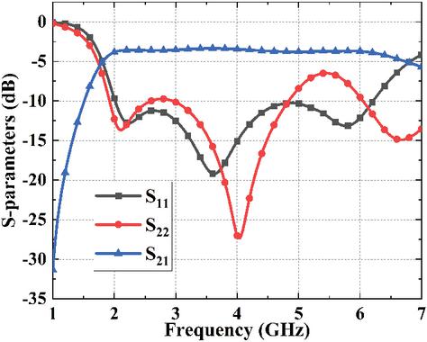
Figure 11 Simulation result of parameters for the output matching circuit.
4.2 Input matching circuit
In terms of the input matching circuit, the matching circuit is constructed by equalizing four two-cell merge circuits for the tube core, and the structure is shown in Fig. 12. The input circuit is realized using a m GaAs monolithic process to equalize the input signal into four two-cell transistor ports, with the output impedance of each circuit set to , and the output impedance of the four parallel combined circuits is .
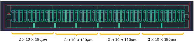
Figure 12 Schematic diagram of an eight-cell transistor core divided into four equal paths.
The input matching circuit construction method is similar to the output matching circuit, in order to ensure a wide bandwidth of low insertion loss and the overall gain of the amplifier within the bandwidth, the use of type microstrip line structure, loading capacitors and other passive components to build matching network, the circuit is shown in Fig. 13. It can be seen that the input matching circuit consists of a series RC structure corresponding to the impedance of the core, the imaginary part of the compensation network constructed by the bonding alloy wire and the bias feed circuit, the third-order L-type impedance transformation network and the power synthesis network. Among them, and are equivalent to the input impedance of the double-cell core, is the equivalent inductance introduced by the bonding alloy wire, and the parallel inductance plays the role of gate bias power supply while it is used to offset the imaginary part of the core impedance capacitance . To improve the matching bandwidth, a three-stage low-pass impedance conversion network is used, and the microstrip lines TL1 and TL2 play the role of impedance conversion and power synthesis at the same time.
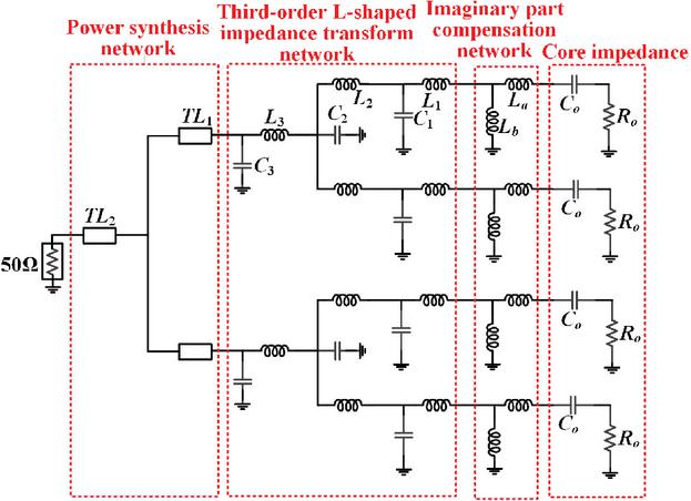
Figure 13 Input matching circuit structure.
Table 2 Dimensions of microstrip lines in the input matching circuit
| Microstrip Line | Dimension (m) | Microstrip Line | Dimension (m) |
| 80667 | 13550 | ||
| 82050 | 179050 | ||
| 87050 | 26050 | ||
| 54850 | 12862000 | ||
| 28950 | 46350 | ||
| 60265 | 20265 | ||
| 34765 | 18765 | ||
| 58265 | 14165 | ||
| 300100 | 1000100 | ||
| 1000100 |
The structure of the input matching circuit is shown in Fig. 14, and the dimensions of each microstrip line are shown in Table 2.
The above input matching, tube core and output matching modules are cascaded to construct the overall circuit structure of the amplifier, and the circuit structure is shown in Fig. 15. Based on the transistor small-signal model and the S-parameters extracted from the output matching circuit, the S-small-signal simulation circuit of the amplifier is constructed. The impedance of input port 1 is . The small-signal simulation results of the amplifier are shown in Fig. 16, and the output port is better than dB in the range of GHz, the input is better than about dB in the band range of GHz, and the gain is better than dB in the range of GHz.
Figure 14 Structure and layout of input matching circuit.
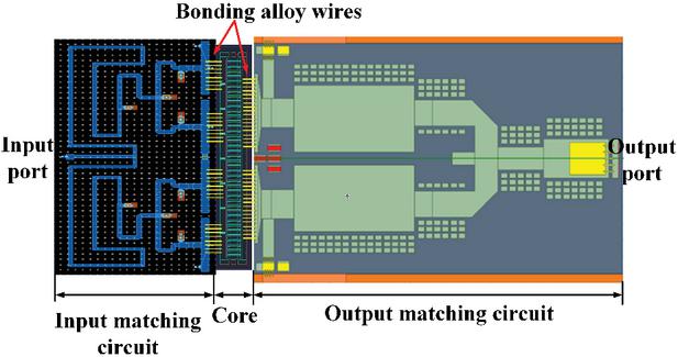
Figure 15 Circuit structure of the GHz quasi-monolithic amplifier.
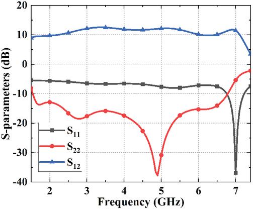
Figure 16 Simulation results of , , and parameters with a small-signal for the GHz quasi-monolithic amplifier.
5 AMPLIFIER CIRCUIT SIMULATION AND TEST RESULTS
Based on the above amplifier structure, a physical sample is prepared as shown in Figs. 17 and 18, in which the bias voltage is set to V and V. The amplifier is subjected to small-signal testing of S-parameters, gain, and other small-signal performances in the range of GHz, and the small-signal performances are obtained by on-chip testing using a vector network analyzer and so on. The small-signal test and simulation results of the amplifier are shown in Fig. 19, and the measured results show that the amplifier fluctuates between dB in the GHz range.
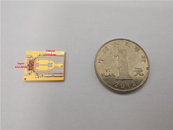
Figure 17 A sample of matching circuit.
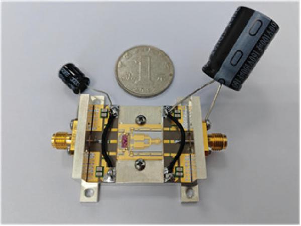
Figure 18 A sample of the GHz quasi-monolithic amplifier.
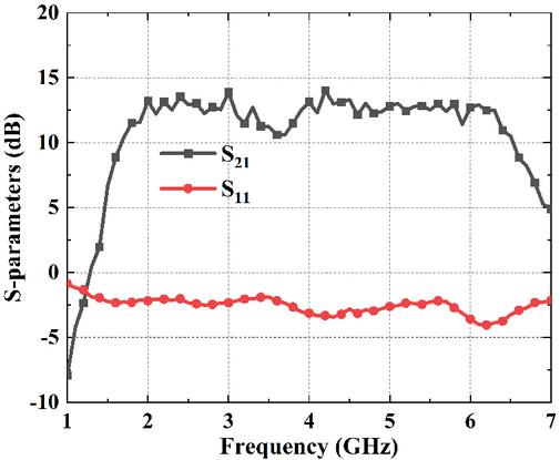
Figure 19 Simulation results of and parameters with a small-signal for the GHz quasi-monolithic amplifier.
The large-signal test of the amplifier is conducted to measure the output power and saturated power added efficiency of the amplifier at the GHz band. The block diagram of the large-signal test connection and the test results are shown in Fig. 20. From the test results, it can be seen that the saturated output power of the amplifier is in the range of dBm in the GHz range, and the gain additive efficiency PAE is .
Table 3 Performance summary and comparison of different distributed amplifiers
| Reference | Frequency (GHz) | Gain (dB) | (dBm) | PAEmax (%) | Bandwidth (%) | FoM | Technology |
| [27] | 1.8-3.2 | 9.0 | 41.4 | 36.0 | 56.0 | 83.4 | 250-nm GaN |
| [28] | 8.4-9.8 | 7.4 | 50.4 | 36.0 | 15.4 | 85.2 | 250-nm GaN |
| [29] | 1.0-1.6 | 10.5 | 47.0 | 27.0 | 46.0 | 88.4 | GaN HEMT |
| [30] | 5.5-6.5 | 12.5 | 44.0 | 40.0 | 16.7 | 84.7 | 250-nm GaN |
| [31] | 8.4-8.6 | 5.0 | 35.0 | 45.0 | 2.3 | 60.1 | GaN HEMT |
| [32] | 2.0-4.0 | 9.8 | 46.5 | 38.0 | 33.3 | 87.3 | 500-nm GaN |
| This Work | 2.0-6.0 | 11.0 | 48.0 | 34.0 | 100.0 | 94.3 | 350-nm GaN |
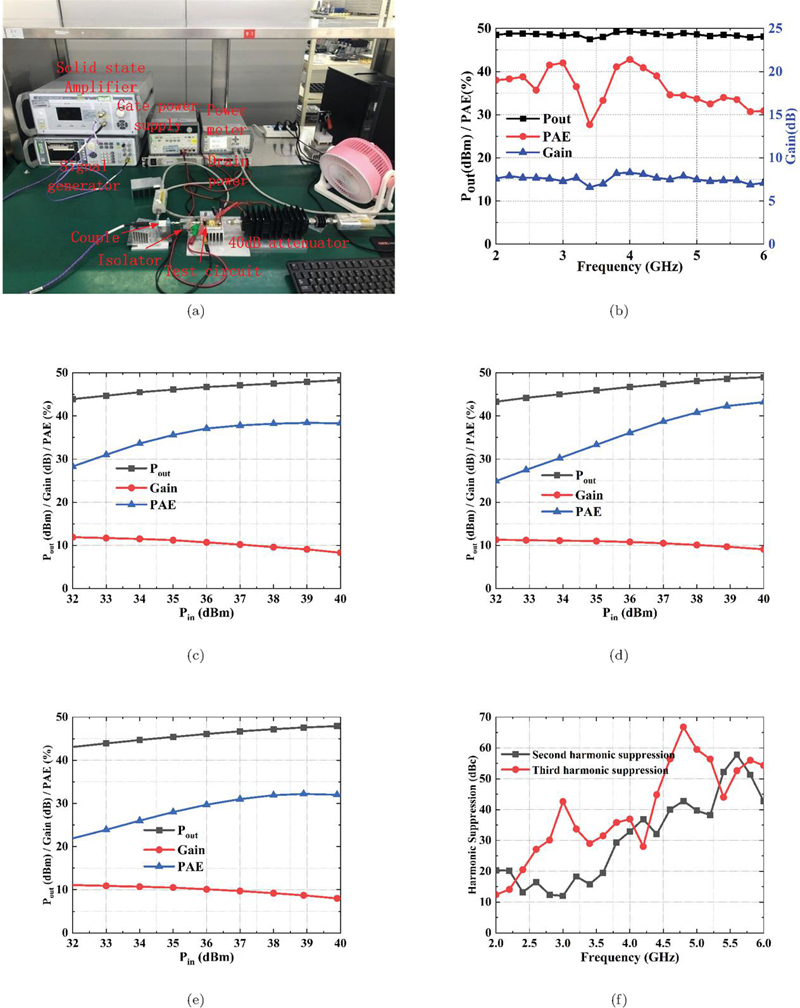
Figure 20 Test results for the performance of the proposed PA. (a) Test setup. (b) Changes of , gain, and PAE as a function of frequency. (c) Changes of , gain, and PAE in terms of at 2.0 GHz. (d) Changes of , gain, and PAE in terms of at 4.0 GHz. (e) Changes of , gain, and PAE in terms of at 6.0 GHz. (f) Suppression effect of harmonic waves.
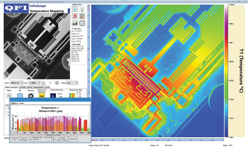
Figure 21 Test result of thermal distribution for the 2-6 GHz quasi-monolithic amplifier.
The performances of this PA is compared with other quasi-monolithic microwave integrated circuit (MMIC) ultra-wideband GaN PAs available in literature [21, 22, 23, 24, 25, 26] and the result is shown in Table 3. The proposed PA can achieve an excellent performance with a bandwidth of GHz, a gain of dB, a saturated output power () of dBm, and a maximum PAE of . Compared with the performance indexes of those PAs from the references, the proposed PA has the highest value of figure of merit (FoM) which is defined by , where is the central frequency of the frequency band.
For the thermal effect of the amplifier, we have conducted a test and the results are shown in Fig. 21. From Fig. 21, we can see that the heat of the amplifier mainly concentrates in the input matching circuit and the maximum temperature is .
6 CONCLUSION
In this paper, a GHz broadband quasi-monolithic amplifier design method is proposed, with the GaN HEMT structure for the tube core, GaAs monolithic microwave integrated circuits for the input matching circuit of the amplifier, and high dielectric constant ceramic substrate for the output matching circuit. The core is a single-cell size gate width of the eight-cell transistor, the output matching circuit will be divided into eight-cell equal to two four-cell core, the input matching circuit will be divided into eight-cell equal to four two-cell core, through the multi-order L-type impedance transformation structure to achieve impedance matching after the design of the combined circuit. The test results show that the amplifier saturates the output power in the range of GHz band at dBm, and the gain added efficiency PAE is .
REFERENCES
[1] M. Garven and J. P. Calame, “Simulation and optimization of gate temperatures in GaN-on-SiC monolithic microwave integrated circuits,” IEEE Transactions on Components and Packaging Technologies, vol. 32, no. 1, pp. 63–72, Mar. 2009.
[2] L. T. Guo, G. J. Deng, S. Y. Xie, H. Shao, W. H. Huang, Y. C. Zhang, Y. J. Zhang, and M. S. Tong, “A miniaturized high-power integrated passive frontend for high-power active array antenna,” IEEE Transactions on Components, Packaging and Manufacturing Technology, vol. 13, no. 11, pp. 1770–1777, Nov. 2023.
[3] Q. Y. Liang and M. S. Tong, “A compensation amplifier with automatic zeroing and stable chopping,” in 2022 IEEE Electrical Design of Advanced Packaging and Systems Symposium, Urbana, Illinois, USA, Dec. 2022.
[4] S. Q. Wang, Y. Y. Hu, and M. S. Tong, “A low-power design of common-mode feedback circuit for fully-differential operational amplifiers,” in 2024 Progress in Electromagnetics Research Symposium, Chengdu, China, Apr. 2024.
[5] H. Kim, I.-J. Yoon, and Y. J. Yoon, “A novel fully integrated transmitter front-end with high power-added efficiency,” IEEE Transactions on Microwave Theory and Techniques, vol. 53, no. 10, pp. 3206–3214, Oct. 2005.
[6] Z. G. Zhou, X. J. Huang, and M. S. Tong, “A 3D circuit model for power distribution networks in complex package structures,” in 2016 IEEE Electrical Design of Advanced Packaging and Systems Symposium, Honolulu, Hawaii, USA, Dec. 2016.
[7] S. C. Wang, M. J. Li, and M. S. Tong, “A miniaturized high-efficiency rectifier with extended input power range for wireless power harvesting,” IEEE Microwave and Wireless Components Letters, vol. 30, no. 6, pp. 617–620, June 2020.
[8] S. C. Wang, M. J. Li, and M. S. Tong, “Wireless power transfer for CubeSats by using a novel high-performance rectenna,” IEEE Antennas and Wireless Propagation Letters, vol. 19, no. 12, pp. 2197–2200, Dec. 2020.
[9] G. Meneghesso, M. Meneghini, A. Tazzoli, N. Ronchi, A. Stocco, A. Chini, and E. Zanoni, “Reliability issues of gallium nitride high electron mobility transistors,” International Journal of Microwave and Wireless Technologies, vol. 2, no. 1, pp. 39–50, Feb. 2010.
[10] R. Sun, J. Lai, W. Chen, and B. Zhang, “GaN power integration for high frequency and high efficiency power applications: A review,” IEEE Access, vol. 8, pp. 15529–15542, 2020.
[11] J. S. Moon, H. Moyer, P. Macdonald, D. Wong, M. Antcliffe, M. Hu, P. Willadsen, P. Hashimoto, C. McGuire, M. Micovic, M. Wetzel, and D. Chow, “High efficiency X-band class-E GaN MMIC high-power amplifiers,” in 2012 IEEE Topical Conference on Power Amplifiers for Wireless and Radio Applications, Santa Clara, CA, USA, Apr. 2012.
[12] S. Pornpromlikit, J. Jeong, C. D. Presti, A. Scuderi, and P. M. Asbeck, “A Watt-level stacked-FET linear power amplifier in silicon-on-insulator CMOS,” IEEE Transactions on Microwave Theory and Techniques, vol. 58, no. 1, pp. 57–64, Jan. 2010.
[13] G. Lee, B. H. Waters, C. Shi, W. S. Park, and J. R. Smith, “Design considerations for asymmetric magnetically coupled resonators used in wireless power transfer applications,” in 2013 IEEE Radio and Wireless Symposium, Austin, TX, USA, Mar. 2013.
[14] M.-D. Tsai, H. Wang, J.-F. Kuan, and C.-S. Chang, “A 70GHz cascaded multi-stage distributed amplifier in 90nm CMOS technology,” 2005 IEEE International Digest of Technical Papers. Solid-State Circuits Conference, San Francisco, CA, USA, Aug. 2005.
[15] G. Nikandish and A. Medi, “Unilateralization of MMIC distributed amplifiers,” IEEE Transactions on Microwave Theory and Techniques, vol. 62, no. 12, pp. 3041–3052, Dec. 2014.
[16] J. C. Chien and L. H. Lu, “40-Gb/s high-gain distributed amplifiers with cascaded gain stages in 0.18-m CMOS,” IEEE Journal of Solid-State Circuits, vol. 42, no. 12, pp. 2715–2725, Dec. 2007.
[17] K. Fang, C. S. Levy, and J. F. Buckwalter, “Supply-scaling for efficiency enhancement in distributed power amplifiers,” IEEE Journal of Solid-State Circuits, vol. 51, no. 9, pp. 1994–2005, Sep. 2016.
[18] J. Kim, H. Park, S. Lee, and Y. Kwon, “6–18 GHz, 8.1 W size-efficient GaN distributed amplifier MMIC,” Electron. Lett., vol. 52, pp. 622–624, 2016.
[19] J. C. Kao, P. Chen, P. C. Huang, and H. Wang, “A novel distributed amplifier with high gain, low noise, and high output power in 0.18-m CMOS technology,” IEEE Transactions on Microwave Theory and Techniques, vol. 61, no. 4, pp. 1533–1542, Apr. 2013.
[20] C. Enz and Y. Cheng, “MOS transistor modeling for RF IC design,” IEEE Journal of Solid-State Circuits, vol. 35, no. 2, pp. 186–201, Feb. 2000.
[21] R. Menozzi, A. Piazzi, and F. Contini, “Small-signal modeling for microwave FET linear circuits based on a genetic algorithm,” IEEE Transactions on Circuits and Systems I: Fundamental Theory and Applications, vol. 43, no. 10, pp. 839–847, Oct. 1996.
[22] L. Zhang, Q.-J. Zhang, and J. Wood, “Statistical neuro-space mapping technique for large-signal modeling of nonlinear devices,” IEEE Transactions on Microwave Theory and Techniques, vol. 56, no. 11, pp. 2453–2467, Nov. 2008.
[23] G. Dambrine, A. Cappy, F. Heliodore, and E. Playez, “A new method for determining the FET small-signal equivalent circuit,” IEEE Transactions on Microwave Theory and Techniques, vol. 36, no. 7, pp. 1151–1159, July 1988.
[24] L. Yang and S. I. Long, “New method to measure the source and drain resistance of the GaAs MESFET,” IEEE Electron Device Letters, vol. 7, no. 2, pp. 75–77, Feb. 1986.
[25] R. Anholt and S. Swirhun, “Equivalent-circuit parameter extraction for cold GaAs MESFET’s,” IEEE Transactions on Microwave Theory and Techniques, vol. 39, no. 7, pp. 1243–1247, July 1991.
[26] A. M. Mangan, S. P. Voinigescu, M.-T. Yang, and M. Tazlauanu, “De-embedding transmission line measurements for accurate modeling of IC designs,” IEEE Transactions on Electron Devices, vol. 53, no. 2, pp. 235–241, Feb. 2006.
[27] R. Quaglia, M. D. Greene, M. J. Poulton, and S. C. Cripps, “A 1.8-3.2-GHz Doherty power amplifier in quasi-MMIC technology,” IEEE Microw. Wireless Compon. Lett., vol. 29, no. 5, pp. 345–347, 2019.
[28] D. Resca and F. Scappaviva, “A minature 70 W quasi-MMIC PA block suitable for highly integrated X-band pulsed SSPA schemes,” in Proceedings of the 11th European Microwave Integrated Circuits Conference, London, UK, Oct. 2016.
[29] D. Bouw, P. Sin, M. Camiade, and J. P. Viaud, “High performance plastic packaged 100 W L-band quasi-MMIC HPA,” in Proceedings of the 46th European Microwave Conference, London, UK, Oct. 2016.
[30] M. Ayad, E. Byk, G. Neveux, M. Camiade, and D. Barataud, “Single and dual input packaged 5.5-6.5 GHz, 20 W, quasi-MMIC GaN-HEMT Doherty power amplifier,” in 2017 IEEE MTT-S International Microwave Symposium, Honololu, HI, USA, June 2017.
[31] J. Jeong, P. Kim, P. Pech, Y. Jeong, and S. Lee, “Quasi-MMIC high power amplifier with silicon IPD matching network,” in Proceedings of the 48th European Microwave Conference, Madrid, Spain, Sep. 2018.
[32] C. Berrached, D. Bouw, M. Camiade, and D. Barataud, “Wideband high efficiency high power GaN amplifiers using MIC and quasi-MMIC technologies,” in Proceedings of the 43rd European Microwave Conference, Nuremberg, Germany, Oct. 2013.
BIOGRAPHIES

Letian Guo received the B.S. degree in electrical engineering from Xi’an Jiaotong University, Xi’an, China, in 2012, the M.S. degree in electromagnetic field and microwave technology from the Northwest Institute of Nuclear Technology, Xi’an, China, in 2015, and the Ph.D. degree in microelectronics and solid-state electronics from Fudan University, Shanghai, China, in 2024, respectively. He has been with the Northwest Institute of Nuclear Technology since 2012. His current research interests include the microwave passive devices and phased array radar technology.

Shunli Ma received the B.S. degree in microelectronics engineering from Shanghai Jiao Tong University, Shanghai, China, in 2011, and the Ph.D. degree in microelectronics engineering from Fudan University, Shanghai, China, in 2016, respectively. From 2012 to 2014, he was a Project Officer with Nanyang Technological University, Singapore. From 2016 to 2017, he worked in industry and designed 77-GHz FMCW PLL for automotive radar sensors. He received the title of Distinguished Designer for millimeter-wave (mm-wave) PLL design for automotive radars. He is currently an Assistant Professor with the State Key Laboratory of ASIC and System, Fudan University, Shanghai, China. He has published many papers related to high-performance mm-wave circuits on top conferences, including ESSCIRC, CICC,RFIC, ASSCC, and IMS. His research interests include 2D MoS2 chip design and mm-wave integrated-circuit design, including mm-wave imaging sensing, mm-wave PLL and high-speed sampler in ADC, and biomedical RF circuits for cancer detection. He received the 2015 ISSCC Student Research Preview and the ISSCC STGA Award.

Hou Yi Ding received the B.S. degree and M.S. degree in microelectronic science and engineering from Tongji University, Shanghai, China, in 2022 and 2025, respectively. He is currently pursuing the Ph.D. degree in Tokyo University, Tokyo, Japan. His current research interests include the development of novel microwave devices and antennas.

Mei Song Tong received the B.S. and M.S. degrees from Huazhong University of Science and Technology, Wuhan, China, and Ph.D. degree from Arizona State University, Tempe, Arizona, USA, all in electrical engineering. He is currently a Humboldt Awardee Professor in the Chair of High-Frequency Engineering, Technical University of Munich, Munich, Germany, and is on leave from the Distinguished/Permanent Professor and Head of Department of Electronic Science and Technology, and Vice Dean of College of Microelectronics, Tongji University, Shanghai, China. He has also held an adjunct professorship at the University of Illinois at Urbana-Champaign, Urbana, Illinois, USA, and an honorary professorship at the University of Hong Kong, China. He has published more than 700 papers in refereed journals and conference proceedings and co-authored eight books or book chapters. His research interests include electromagnetic field theory, antenna theory and technique, modeling and simulation of RF/microwave circuits and devices, interconnect and packaging analysis, inverse electromagnetic scattering for imaging, and computational electromagnetics.
Prof. Tong is a Fellow of the Electromagnetics Academy, Fellow of the Japan Society for the Promotion of Science (JSPS), and Senior Member (Commission B) of the USNC/URSI. He has been the chair of Shanghai Chapter since 2014 and the chair of SIGHT committee in 2018, respectively, in IEEE Antennas and Propagation Society. He has served as an associate editor or guest editor for several well-known international journals, including IEEE Antennas and Propagation Magazine, IEEE Transactions on Antennas and Propagation, IEEE Transactions on Components, Packaging and Manufacturing Technology, International Journal of Numerical Modeling: Electronic Networks, Devices and Fields, Progress in Electromagnetics Research, and Journal of Electromagnetic Waves and Applications. He also frequently served as a session organizer/chair, technical program committee member/chair, and general chair for some prestigious international conferences. He was the recipient of a Visiting Professorship Award from Kyoto University, Japan, in 2012, and from University of Hong Kong, China, 2013. He advised and coauthored 15 papers that received the Best Student Paper Award from different international conferences. He was the recipient of the Travel Fellowship Award of USNC/URSI for the 31th General Assembly and Scientific Symposium (GASS) in 2014, Advance Award of Science and Technology of Shanghai Municipal Government in 2015, Fellowship Award of JSPS in 2016, Innovation Award of Universities’ Achievements of Ministry of Education of China in 2017, Innovation Achievement Award of Industry-Academia-Research Collaboration of China in 2019, “Jinqiao” Award of Technology Market Association of China in 2020, Baosteel Education Award of China in 2021, Carl Friedrich von Siemens Research Award of the Alexander von Humboldt Foundation of Germany in 2023, and Technical Achievement Award of Applied Computational Electromagnetic Society (ACES) of USA in 2024. In 2018, he was selected as the Distinguished Lecturer (DL) of IEEE Antennas and Propagation Society for 2019–2022, and in 2025, he was selected to the Top Scientists List for both Career-Long Impact and Single-Year Impact by ELSEVIER and Stanford University.
ACES JOURNAL, Vol. 40, No. 10, 1010–1020
DOI: 10.13052/2025.ACES.J.401006
© 2025 River Publishers