Low-Loss 16-Way Ultra-Wideband Wilkinson Power Divider
Jorge A. Caripidis Troccola1, Satheesh Bojja Venkatakrishnan1, Cedric W. L. Lee2, Theng Huat Gan2, and John L. Volakis1
1Department of Electrical Engineering
Florida International University, Miami, FL, 33174, USA
jcari006@fiu.edu, sbojjave@fiu.edu, jvolakis@fiu.edu
2National University of Singapore, Singapore 117411
c.lee@nus.edu.sg, thenghuat@nus.edu.sg
Submitted On: June 17, 2025; Accepted On: November 24, 2025
Abstract
Several power divider designs exist in the literature and are also commercially available. However, these dividers are not wideband. In this paper, a low-loss, ultra-wideband (UWB) 16-way power divider for UWB applications is presented. Notably, the design employs 15 cascaded multi-stage Wilkinson power dividers with a total of 90, 0402 package surface mounted chip resistors to enable operation from 0.2 to 3.6 GHz. Remarkably, the fabricated prototype achieves an 18:1 input and output impedance bandwidth with VSWR 1.2 thanks to an optimization approach that eliminates any additive reflection from each of the power division stages. In addition, the maximum insertion loss is 3 dB at the highest frequency of operation, while the maximum phase imbalance between output ports is 4 degrees. The measurements show excellent agreement with the simulations.
Keywords: Feed network, power divider, ultra-wideband, Wilkinson..
1 INTRODUCTION
Power dividers are essential components in RF and microwave systems, enabling signal splitting for various applications, including telecommunications, radar, and wireless communication systems [1]. Their role is to distribute signals equally or with specified ratios across multiple pathways. Power dividers are generally classified into a few types: resistive, T-Junction, Wilkinson, and hybrid. A typical limitation among these dividers is their narrow bandwidth, which makes them unsuitable for bandwidth demanding applications [2]. In modern ultra-wideband (UWB) systems, it is crucial to have a power divider that can operate over a broad range of frequencies (2:1) while maintaining low insertion loss [3], good port isolation, and minimal phase imbalance. For instance, in the phase-array designs presented in [4, 5, 6, 7, 8], a power divider with the specified characteristics could serve as an effective feeding network. Other practical scenarios where UWB power dividers can be beneficial include high precision imaging and positioning systems [9, 10].
Different designs to extend the bandwidth of power dividers have been explored. For example, in [11], a two-way, multilayer slotline power divider was shown to operate from 3.1 to 10 GHz. Additionally, in [12], a microstrip power divider using a pair of stepped-impedance open-circuited stubs and parallel coupled lines achieved a bandwidth ratio of 3.4:1. Moreover, a feed network design consisting of cascaded three-stage Wilkinson power dividers was used to feed a 16-element phased antenna array across 5 to 30 GHz [13]. Also, in [14], an 8-way power divider with printed carbon ink resistors and tapered microstrip lines operated from 0.5 to 25 GHz. While these designs increased the operational bandwidth as compared to traditional power dividers, there are still some shortcomings. For instance, the designs from [11] and [12] achieved a bandwidth ratio of only 3.4:1 and for only two output ports. The design presented in [13] increased the number of output ports to 16 with a bandwidth ratio of 6:1. However, 6:1 is still not large enough for some demanding UWB applications. Lastly, the 8-way resistive power divider from [14] achieved a bandwidth ratio of 50:1, but suffered from an insertion loss of up to 7 dB at the high band. With respect to [13] and [14], our proposed design provides improvement in bandwidth and a 4 dB improvement in insertion loss at higher bands, respectively.
To concurrently achieve large bandwidth, low loss, and high number of output ports, this paper introduces a 16-way power divider that exhibits 18:1 bandwidth and very low insertion loss across the frequency band. Notably, the proposed design is structured using a series of 15 cascaded multi-stage Wilkinson power dividers, each optimized for low insertion loss and high impedance bandwidth. By incorporating a total of 90, 0402 chip resistors, the design is able to operate from 0.2 GHz to 3.6 GHz. The power divider’s input and output impedance port matching are further optimized to mitigate reflective losses that could otherwise accumulate across the cascading stages.
The optimized architecture yields significant performance benefits, achieving a maximum insertion loss of only 3 dB at the highest operational frequency while maintaining the phase imbalance between output ports below 4 degrees. These characteristics make the proposed power divider highly attractive for UWB array feeding. A prototype was fabricated and measured to verify the performance. The following sections present the design methodology, implementation details, prototype fabrication, and performance analysis. A 16-port power divider achieving a bandwidth ratio greater than , while maintaining low insertion loss and minimal phase imbalance, is not commonly found in the literature. This work contributes a novel solution addressing these challenges within a compact and optimized architecture.
2 POWER DIVIDER DESIGN AND SIMULATION
2.1 Design considerations
In a traditional Wilkinson divider, the circuit splits the input power into two equal outputs through quarter-wave transmission line sections that transform the output impedance back to the input impedance. For a simple two-way divider, the impedance of each quarter wave transformer/leg is chosen as [15]:
| (1) |
where is the characteristic impedance of the overall system (typically 50 ). This impedance transformation ensures that each output port maintains a matched condition with respect to the input, minimizing reflections. Furthermore, a resistor connecting the two output ports (of value 2) absorbs any potential imbalances in power or phase between the outputs, providing isolation and preventing undesired coupling [15, 16]. Notably, a single-stage Wilkinson power divider, while effective for narrowband applications, cannot maintain low VSWR and consistent performance across ultra-wideband frequencies. This limitation arises due to the quarter-wave impedance transformation only working optimally at a specific frequency, leading to increased mismatches and higher losses outside a narrow range.
The design of each 1-to-2 Wilkinson cell division followed a systematic procedure to balance bandwidth and complexity. First, the target operating band was defined, and the center frequency was set as , with all quarter-wave lines designed to be at . To determine the minimum number of sections, m, we began with a single quarter-wave section and evaluated the simulated return loss across the band. If the response did not meet the expected return-loss target ( dB), more sections were added. The smallest m value that satisfied the set specification was selected to minimize both insertion loss and layout complexity.
For a single-section divider, the quarter-wave impedance per branch was set to with a single isolation resistor of placed between the output ports. For the multi-section designs, a progression of impedances were employed to realize the gradual transformation from to . Correspondingly, multiple resistors were distributed along the arms such that their combined effect maintained approximately isolation at the design frequency. This distribution provided a flatter isolation response across the wideband range as compared to using a single lumped resistor.
Each impedance value was then translated into physical microstrip dimensions using standard microstrip equations. To further suppress parasitic reflections, adjacent sections were connected using short linear tapers rather than abrupt width steps. The final optimization values were performed through circuit simulations to ensure that the bandwidth, insertion loss, return loss, and isolation targets were simultaneously achieved.
To overcome bandwidth limitations, a multi-stage Wilkinson power divider design is adopted. The proposed design uses a six-stage (meaning each cell includes six resistors) Wilkinson divider structure within each of the 15 cascaded cells. This approach divides the power sequentially in steps, achieving incremental impedance transformations that enable the divider to achieve large bandwidths. The layout of the proposed divider is shown in Fig. 1.
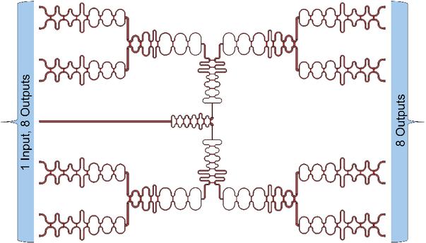
Figure 1 Layout of the proposed 16-way power divider.
2.2 Geometry optimization for UWB performance
In the initial design phase of the 16-way power divider, we followed a modular approach that consisted in creating a single six-stage, two-way Wilkinson power divider unit cell able to operate from 0.2 to 3.6 GHz. These identical unit cells were then cascaded in a sequential manner, ultimately obtaining 16 outputs, by continuously splitting the signal in stages, as shown in Fig. 2.
However, this approach encountered significant challenges in a practical implementation, as evidenced by the input VSWR shown in Fig. 2. Specifically, the input VSWR plot reveals a resonance at 0.6 GHz and many more higher frequency resonances, which degraded the input matching significantly across the band. These resonances were caused by cumulative reflections that emerged due to the repeated cascading of identical unit cells. These mismatches added to one another at certain frequencies where the phase alignment of reflected signals reinforced each other. As these reflections compounded, they introduced strong resonances within the VSWR, ultimately compromising the bandwidth and performance of the divider.
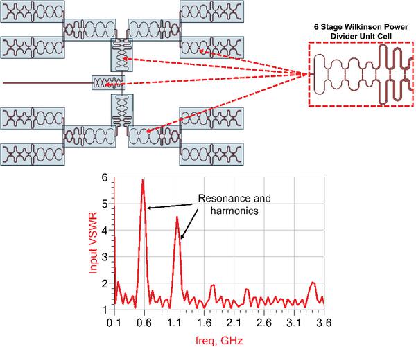
Figure 2 Details of modular design with identical unit cells and VSWR performance. Cumulative reflection creates resonance at 0.6 GHz and its corresponding harmonics.
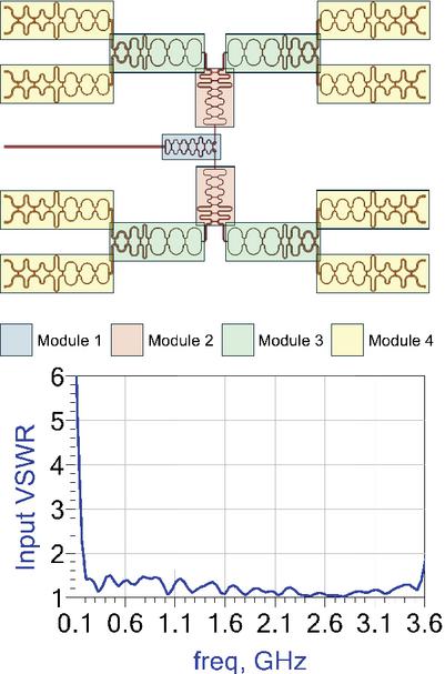
Figure 3 Optimized design layout and VSWR performance of 16-way power divider operating from 0.2 to 3.6 GHz. Each stage of the power division, represented by different colored modules, is composed of a series of unique, optimized, two-way, six-stage Wilkinson power dividers. Any cumulative reflection is eliminated.
To address the resonances, we implemented a geometry optimization process for each stage of the divider. Rather than using identical unit cells, we optimized several design parameters for each individual power splitting section within the division stages, creating four unique modules represented by colors in Fig. 3. This careful adjustment provided a unique impedance transformation for each stage, breaking the repetitive pattern that had previously led to resonances. The schematic of the design’s modules is shown in Fig. 4, with the component values and dimensions detailed in Tables 1 through 5.
In the optimization process, multiple design parameters were strategically selected. The width and length of each line segment were calculated to maintain impedance matching across the operating band. In addition, gradual tapering in certain transmission line sections was introduced to facilitate smooth impedance transitions. This technique minimized abrupt impedance changes between sections, reducing reflection and enhancing bandwidth. Furthermore, the values of the 0402 chip resistors were optimized at each stage to absorb any imbalances and provide effective isolation between adjacent outputs. The resistors prevent inter-port coupling by dissipating unwanted signals, ensuring isolation as well as phase stability across the wide bandwidth. Moreover, the distance between consecutive sections was also adjusted to reduce coupling and minimize reflections. Importantly, each section of the power divider was meandered in order to reduce the size of the structure, as depicted in Fig. 4. Overall, the meticulous optimization created a distinct impedance transformation at each stage, effectively disrupting the repetitive structural pattern and eliminating cumulative reflections that had previously led to resonances.
Table 1 Two step optimization process
| Parameter Category | Initial Values (Through Derivation) | Constraints in Optimization |
| Transmission line widths | Calculated from closed-form microstrip equations for each impedance | Limited by available substrates and manufacturing pitch (min trace width mil) |
| Transmission line lengths | Set to at center frequency | Tuned within during circuit optimization |
| Isolation resistors | Set to (single-section), and distributed for multi-section arms | Adjusted within during circuit optimization |
| Number of sections per arm | Determined by return-loss target | Limited to to minimize complexity |
| Cascading strategy | Initially, identical 1-to-2 cells. Further optimized based on their dependence to previous stages | Fixed 16-way network topology |
Table 2 Microstrip transmission lines dimensions
| Components | Module 1 | Module 2 | Module 3 | Module 4 | ||||
| W (mm) | L (mm) | W (mm) | L (mm) | W (mm) | L (mm) | W (mm) | L (mm) | |
| MTL1 | 1.69 | 117.22 | 0.87 | 1.80 | 1.13 | 0.78 | 2.05 | 0.76 |
| MTL2 | 0.54 | 2.94 | 0.28 | 5.80 | 0.36 | 4.26 | 0.65 | 2.25 |
| MTL3 | 0.54 | 0.31 | 0.28 | 2.58 | 0.36 | 1.10 | 0.65 | 0.31 |
| MTL4 | 0.54 | 1.69 | 0.28 | 1.97 | 0.33 | 1.86 | 0.65 | 1.01 |
| MTL5 | 0.48 | 0.30 | 0.30 | 1.80 | 0.53 | 0.67 | 0.31 | 0.67 |
| MTL6 | 0.48 | 0.30 | 0.30 | 0.32 | 0.53 | 0.67 | 0.31 | 0.67 |
| MTL7 | 0.48 | 1.58 | 0.46 | 1.89 | 0.53 | 1.74 | 0.31 | 0.95 |
| MTL8 | 0.75 | 0.31 | 0.47 | 0.58 | 0.71 | 1.04 | 0.78 | 1.33 |
| MTL9 | 0.75 | 0.31 | 0.47 | 0.90 | 0.71 | 1.66 | 0.78 | 0.92 |
| MTL10 | 0.75 | 1.58 | 0.47 | 1.90 | 0.87 | 7.33 | 0.85 | 1.14 |
| MTL11 | 0.59 | 1.58 | 0.47 | 1.90 | 0.87 | 7.27 | 0.85 | 0.95 |
| MTL12 | 0.59 | 0.73 | 0.46 | 1.77 | 0.87 | 1.56 | 0.85 | 0.87 |
| MTL13 | 0.59 | 1.54 | 0.46 | 1.77 | 0.87 | 1.56 | 0.85 | 0.87 |
| MTL14 | 0.82 | 2.30 | 0.71 | 7.46 | 1.12 | 3.82 | 1.00 | 1.04 |
| MTL15 | 0.82 | 1.58 | 0.71 | 1.68 | 1.12 | 3.92 | 1.00 | 2.20 |
| MTL16 | 0.82 | 1.58 | 0.71 | 1.68 | 1.12 | 3.92 | 1.00 | 2.20 |
| MTL17 | 0.55 | 0.73 | 0.53 | 1.58 | 0.71 | 0.66 | 1.19 | 3.20 |
| MTL18 | 0.55 | 0.73 | 0.53 | 0.63 | 0.71 | 0.66 | 1.19 | 3.20 |
| MTL19 | 0.55 | 0.83 | 0.53 | 1.58 | 0.71 | 0.66 | 1.19 | 3.20 |
| MTL20 | 0.87 | 0.38 | 1.13 | 2.05 | 0.30 | 1.43 | 0.30 | 1.43 |
Table 3 Microstrip T-Junction dimensions
| Components | Module 1 (mm) | Module 2 (mm) | Module 3 (mm) | Module 4 (mm) | ||||||||
| W1 | W2 | W3 | W1 | W2 | W3 | W1 | W2 | W3 | W1 | W2 | W3 | |
| MTJ1 | 0.54 | 0.54 | 1.69 | 0.28 | 0.28 | 0.87 | 0.36 | 1.13 | 0.65 | 0.65 | 2.05 | 0.85 |
| MTJ2 | 0.54 | 0.48 | 0.54 | 0.28 | 0.30 | 0.28 | 0.53 | 0.41 | 0.65 | 0.67 | 0.65 | 0.65 |
| MTJ3 | 0.48 | 0.75 | 0.48 | 0.30 | 0.47 | 0.48 | 0.71 | 0.53 | 0.67 | 0.78 | 0.67 | 0.67 |
| MTJ4 | 0.75 | 0.59 | 0.75 | 0.47 | 0.46 | 0.47 | 0.87 | 0.71 | 0.85 | 0.85 | 0.78 | 0.85 |
| MTJ5 | 0.59 | 0.82 | 0.59 | 0.46 | 0.71 | 0.46 | 1.12 | 0.87 | 1.00 | 1.00 | 0.85 | 1.00 |
| MTJ6 | 0.82 | 0.55 | 0.82 | 0.71 | 0.89 | 0.71 | 1.12 | 1.12 | 1.00 | 1.19 | 1.00 | 1.19 |
| MTJ7 | 0.55 | 1.24 | 0.55 | 0.89 | 1.24 | 0.89 | 1.53 | 1.24 | 1.19 | 1.43 | 1.19 | 1.19 |
Table 4 Curved microstrip transmission lines dimensions
| Components | Module 1 (mm) | Module 2 (mm) | Module 3 (mm) | Module 4 (mm) | ||||||||
| W | (∘) | R | W | (∘) | R | W | (∘) | R | W | (∘) | R | |
| MC1 | 0.54 | 180 | 1.51 | 0.28 | 180 | 2.16 | 0.36 | 180 | 5.08 | 25.56 | 180 | 4.17 |
| MC2 | 0.54 | 90 | 1.27 | 0.28 | 90 | 1.27 | 0.36 | 90 | 1.36 | 25.56 | 90 | 1.37 |
| MC3 | 0.48 | 90 | 1.27 | 0.30 | 90 | 1.27 | 0.53 | 90 | 1.36 | 26.40 | 90 | 1.37 |
| MC4 | 0.48 | 180 | 1.51 | 0.30 | 180 | 2.16 | 0.53 | 180 | 5.08 | 26.40 | 180 | 4.17 |
| MC5 | 0.48 | 90 | 1.27 | 0.30 | 90 | 1.27 | 0.53 | 90 | 1.36 | 30.58 | 90 | 1.37 |
| MC6 | 0.75 | 90 | 1.27 | 0.47 | 90 | 1.27 | 0.71 | 90 | 1.36 | 30.58 | 90 | 1.37 |
| MC7 | 0.75 | 180 | 1.51 | 0.47 | 180 | 2.16 | 0.71 | 180 | 5.08 | 30.58 | 180 | 4.17 |
| MC8 | 0.75 | 90 | 1.27 | 0.47 | 90 | 1.27 | 0.71 | 90 | 1.36 | 33.51 | 90 | 2.71 |
| MC9 | 0.59 | 90 | 1.35 | 0.46 | 90 | 1.28 | 0.87 | 90 | 1.27 | 33.51 | 90 | 2.71 |
| MC10 | 0.59 | 180 | 1.51 | 0.46 | 180 | 1.27 | 0.87 | 180 | 2.84 | 39.53 | 180 | 3.77 |
| MC11 | 0.59 | 90 | 1.27 | 0.46 | 90 | 1.28 | 0.87 | 90 | 1.27 | 39.53 | 90 | 3.77 |
| MC12 | 0.59 | 90 | 1.27 | 0.71 | 90 | 1.28 | 1.12 | 90 | 1.27 | 39.53 | 90 | 3.77 |
| MC13 | 0.82 | 180 | 1.27 | 0.71 | 180 | 1.43 | 1.12 | 180 | 2.84 | 46.77 | 180 | 3.77 |
| MC14 | 0.82 | 90 | 1.27 | 0.71 | 90 | 1.27 | 1.12 | 90 | 1.27 | 46.77 | 90 | 3.77 |
| MC15 | 0.55 | 90 | 1.27 | 0.89 | 90 | 1.28 | 1.53 | 90 | 1.27 | 46.77 | 90 | 3.77 |
| MC16 | 0.55 | 180 | 1.27 | 0.89 | 180 | 1.43 | 1.53 | 180 | 2.84 | 56.14 | 180 | 3.77 |
| MC17 | 0.55 | 90 | 1.27 | 0.89 | 90 | 1.28 | 1.53 | 90 | 1.27 | 56.14 | 90 | 3.77 |
| MC18 | 2.33 | 90 | 1.27 | 1.24 | 90 | 1.28 | 1.24 | 90 | 1.27 | 56.14 | 90 | 3.77 |
Table 5 Tapered microstrip transmission lines dimensions
| Components | Module 1 (mm) | Module 2 (mm) | Module 3 (mm) | Module 4 (mm) | ||||||||
| W1 | W2 | L | W1 | W2 | L | W1 | W2 | L | W1 | W2 | L | |
| MTP1 | 0.55 | 0.87 | 0.32 | 1.24 | 1.13 | 0.31 | 0.54 | 2.05 | 0.31 | 1.43 | 1.69 | 1.57 |
Table 6 0402 resistor values
| Components | Module 1 | Module 2 | Module 3 | Module 4 |
| Resistance () | Resistance () | Resistance () | Resistance () | |
| R1 | 150.00 | 150.00 | 150.00 | 261.00 |
| R2 | 261.00 | 154.00 | 180.00 | 300.00 |
| R3 | 300.00 | 267.00 | 242.00 | 300.00 |
| R4 | 348.00 | 294.00 | 348.00 | 348.00 |
| R5 | 300.00 | 300.00 | 300.00 | 300.00 |
| R6 | 300.00 | 300.00 | 100.00 | 300.00 |

Figure 4 Top to bottom: Power divider module schematic and Module 4 sample layout (notice meandering and tapering).
2.3 Simulations
Simulations of the optimized design from Fig. 3 are shown in Fig. 5. A two-step optimization process was applied to refine the divider design. The first, circuit-level simulations were performed in Keysight’s ADS, where the cascaded 1-to-2 Wilkinson cells were optimized based on the starting values described in section II, part B. The optimization was carried out in a sequential manner, with each subsequent cell tuned while accounting for the response of the preceding stage. In this manner, no two cells remained identical in the final implementation. The latter was key to suppressing cumulative impedance mismatches and potential resonances.
Once the complete 16-way structure was finalized at the circuit level, the layout was transferred into Ansys HFSS for full-wave electromagnetic simulation. This final validation ensured that electromagnetic coupling, discontinuities, and higher-order effects were properly captured. The initial design parameters used in the optimization process were not arbitrarily selected but were derived from the synthesis procedure outlined in section II, part B (resistor selection, microstrip line width/length calculation, taper calculation, etc.). Table 1 summarizes the key parameter categories and the constraints applied during optimization.
As shown in Fig. 5, the design operates from 0.20 to 3.6 GHz and demonstrates an impressive 18:1 bandwidth with an input VSWR 1.5 and an output VSWR 1.8. Furthermore, the design achieves an insertion loss of only 2 dB higher than that of an ideal 16-way power divider. Additionally, the port isolation is excellent, except for neighboring ports, where the isolation is 10 dB.
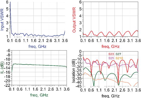
Figure 5 Simulated input VSWR, output VSWR, insertion loss, and port isolation of the optimized, modular design from Fig. 3.
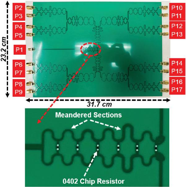
Figure 6 Details of the fabricated 16-way power divider prototype.
3 PROTOTYPE FABRICATION AND MEASUREMENTS
3.1 Fabricated prototype
A prototype of the optimized, 16-way Wilkinson power divider from Fig. 3 was fabricated on a Rogers 4350B substrate [17]. The substrate was selected for its suitable dielectric properties in high-frequency applications, featuring a relative permittivity of , a loss tangent , and a total thickness of 0.76 mm.
The fabrication process involved the precise placement of 90 surface-mounted resistors in 0402 packages. Specifically, the 0402 resistor package size was chosen to be in compliance with the microstrip trace size. An automated pick-and-place machine was employed to position the resistors, ensuring consistent alignment and reliable electrical contact. Notably, these resistors played a critical role in isolating output ports to maintain uniform performance across the broad bandwidth. For measurements, 17 SMA connectors were hand-soldered to the prototype. One connector was placed at the input port and 16 at the output ports. The fabricated prototype is shown in Fig. 6.
Notably, resistor tolerances and placement errors can introduce measurable amplitude and phase imbalances in power dividers, particularly in Wilkinson configurations. These variations were modeled and considered in our circuit-level and full wave electromagnetic simulation. Specifically, the deviations in values were imported from the datasheets of commercially available 0402 resistors. For example, a ±5% tolerance in the isolation resistor can lead to amplitude imbalances of up to ±0.4 dB and phase errors approaching ±5∘[18], especially near the upper end of the operating frequency range. Placement inaccuracies, such as a 0.2 mm shift in resistor location or misalignment in microstrip geometry, can further increase mismatch, leading to degraded return loss and isolation performance. Simulations show that a shift of 0.2 mm in resistor placement within the transmission line can result in an increase of the insertion loss by 0.85 dB across the design frequency range.
Further, dielectric substrates used in microstrip circuits, such as FR4, Rogers 4350, and alumina (Al2O3), also impose power limitations governed by their thermal conductivity and dielectric breakdown thresholds. Standard substrates like FR4 and Ro4350 can only handle a few watts due to poor thermal dissipation, while advanced ceramics such as alumina and aluminum nitride (AlN) can support power levels approaching 1–2 kW when paired with wide transmission lines and effective heat sinking. Nevertheless, MW-level power handling remains beyond the scope of microstrip technology and instead requires waveguide-based architectures, vacuum electron devices, and metal-ceramic structures.
3.2 Measurements
The performance of the fabricated 16-way Wilkinson power divider was measured using an E5071C ENA Vector Network Analyzer (VNA). The VNA measurements focused on evaluating several critical performance metrics, including port VSWR, insertion loss, isolation between output ports, and phase imbalance across the output ports. These measurements are plotted vs simulations in Fig. 7.
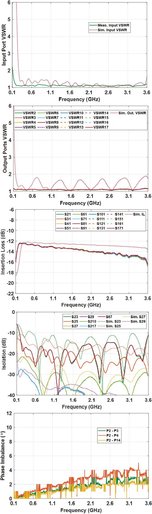
Figure 7 Measured input VSWR, output VSWR, insertion loss, port isolation, and phase imbalance of the fabricated prototype from Fig. 6. Measured results are depicted in solid lines, while dotted lines present the simulation data.
For the VSWR measurements, both input and output ports were evaluated to ensure impedance matching across the intended frequency range. As seen in Fig. 7, the measured input VSWR matches simulations, whereas the measured output VSWR is better than expected, verifying UWB operation from 0.2 to 3.6 GHz. In addition, the insertion loss was measured at every output port to assess the divider’s efficiency in power distribution. Measurements of the insertion loss show good agreement with simulations. However, a slight drop in performance is seen as the frequency increases, where measurements exhibit an extra 1–2 dB of loss on average as compared to the simulations. This could be due to ohmic losses being more prevalent at high frequencies.
At upper bands, insertion loss in power dividers and similar RF structures often exceeds expected values based on ohmic losses alone. While conductor (ohmic) loss due to skin effect increases with frequency, its contribution is usually limited to dB/inch on standard copper microstrip lines [19]. However, conductor surface roughness becomes a major contributor at these frequencies. For example, rough copper with RMS height m can increase effective resistance by 10-20 %, leading to additional losses of 0.5–1 dB/inch. Similarly, dielectric losses contribute meaningfully; for instance, Rogers RO4350B ( at 10 GHz) can cause 0.1–0.3 dB/inch loss [17], and material variability or temperature-induced dielectric drift can introduce further imbalance and phase error. Moreover, connector transitions and launch structures (e.g., SMA to microstrip) can add another 0.3–-0.7 dB per interface due to imperfect impedance matching and ground continuity [20].
Still, the overall worst-case measured insertion loss is only 3 dB higher than the expected ideal 16-way power divider. To examine isolation between ports, measurements were taken across various port combinations. These included both neighboring ports and those spaced farther apart. As displayed in the isolation plots, measured curves show a slightly better performance across the whole band of operation, with the lowest isolation between neighboring ports being 15 dB. Finally, phase imbalances across the output ports were measured by assessing multiple port combinations. Both adjacent and distant port pairs were analyzed to determine the uniformity of the phase distribution. As seen from the plot, a maximum phase imbalance of 4 degrees was measured. We observed similar phase imbalance in all ports. This imbalance is well within acceptable limits, validating the divider’s effectiveness in achieving stable phase performance across all output ports.
4 CONCLUSION AND REMARKS
This work demonstrated the design, fabrication, and validation of a 16-way ultra-wideband Wilkinson power divider. The paper addressed the challenges of achieving a large number of ports for antenna array feeding across a wideband performance. Its wide bandwidth offers a clear potential for next-generation phased arrays and broadband RF systems, where uniform power distribution is essential. While the cascaded multi-stage approach was effective, some practical issues were observed, including sensitivity to resistor tolerances, complexity of the layout, and unoptimized power handling capability. These issues may restrict scalability and high-power operation. Future efforts could explore architecture simplification to enhance power handling as well as extend the concept to millimeter-wave frequencies and reconfigurable environments. Overall, the results establish a strong foundation for compact, wideband power division networks that can support the evolving demands of modern communication and sensing technologies.
References
[1] D. M. Pozar, Microwave Engineering, 3rd ed. Hoboken, NJ, USA: Wiley, 2005, ch. 7, pp. 317–380.
[2] Microstrip and CPW Power Divider Design PathWave Advanced Design System (ADS). Available: https://www.keysight.com/us/en/assets/7018-05297/technical-overviews/5992-1632.pdf
[3] Microstrip Loss Calculations, https://www.microwaves101.com/encyclopedias/microstrip-loss-calculations
[4] M. Carvalho, A. D. Johnson, E. A. Alwan, and J. L. Volakis, “Semi-Resistive Approach for Tightly Coupled Dipole Array Bandwidth Enhancement,” IEEE Open Journal of Antennas and Propagation, vol. 2, pp. 110–117, 2021.
[5] A. D. Johnson, J. Zhong, S. B. Venkatakrishnan, E. A. Alwan, and J. L. Volakis, “Phased Array With Low-Angle Scanning and 46:1 Bandwidth,” IEEE Transactions on Antennas and Propagation, vol. 68, no. 12, pp. 7833–7841, Dec. 2020.
[6] J. Zhong, A. Johnson, E. A. Alwan, and J. L. Volakis, “Dual-Linear Polarized Phased Array With 9:1 Bandwidth and 60∘ Scanning Off Broadside,” IEEE Transactions on Antennas and Propagation, vol. 67, no. 3, pp. 1996–2001, Mar. 2019.
[7] M. H. Novak, F. A. Miranda, and J. L. Volakis, “Ultra-wideband phased array for millimeter-wave ISM and 5G bands, realized in PCB,” IEEE Transactions on Antennas and Propagation, vol. 66, no. 12, pp. 6930–6938, Dec. 2018.
[8] J. P. Doane, K. Sertel, and J. L. Volakis, “A wideband, wide scanning tightly coupled dipole array with integrated balun (TCDA-IB),” IEEE Transactions on Antennas and Propagation, vol. 61, no. 9, pp. 4538–4548, Sep. 2013.
[9] F. A. Shaikh and S. Khan, “Design and optimization of ultra-wideband antipodal vivaldi antenna for radar and microwave imaging application,” Sindh University Research Journal (Science Series), vol. 50, no. 3D, pp. 06–09, 2018.
[10] “Why Ultra-Wideband Matters FiRa Consortium,” FiRa Consortium, Sep. 11, 2023. https://www.firaconsortium.org/resource-hub/blog/why-ultrawideband-matters (accessed Oct. 24, 2024).
[11] K. Song and Q. Xue, “Novel ultra-wideband (UWB) multilayer slotline power divider with bandpass response,” IEEE Microwave and Wireless Components Letters, vol. 20, no. 1, pp. 13–15, Jan. 2010.
[12] S. W. Wong and L. Zhu, “Ultra-wideband power divider with good in-band splitting and isolation performances,” IEEE Microwave and Wireless Components Letters, vol. 18, no. 8, pp. 518–520, Aug. 2008.
[13] D. A. Ramirez, W. J. D. Johnson, and G. Mumcu, “Ultra-wideband phased antenna array time delay unit architecture optimization in presence of component non-idealities,” IEEE Open Journal of Antennas and Propagation, vol. 5, no. 4, pp. 994–1003, Aug. 2024.
[14] R. Solanki, P. K. Tan, and T. H. Gan, “Compact ultra-wideband 8-way power divider with printed resistors,” in 2023 Asia-Pacific Microwave Conference (APMC), Taipei, Taiwan, pp. 629–631, 2023.
[15] E. J. Wilkinson, “An N-way hybrid power divider,” IRE Transactions on Microwave Theory and Techniques, vol. 8, no. 8, pp. 116–118, Aug. 1960.
[16] E. J. Wilkinson, “Power divider,” US Patent, No. 3 091 743, Cl. 333-9, 1963.
[17] “RO4350BTM Laminates,” Rogerscorp.com, 2024. https://rogerscorp.com/advanced-electronics-solutions/ro4000-series-laminates/ro4350b-laminates
[18] S. B. Venkatakrishnan, A. Hovsepian, A. D. Johnson, T. Nakatani, E. A. Alwan, and J. L. Volakis, “Techniques for achieving high isolation in RF domain for simultaneous transmit and receive,” IEEE Open Journal of Antennas and Propagation, vol. 1, pp. 358–367, 2020.
[19] https://docs.amd.com/r/en-US/ug583-ultrascale-pcb-design/Dielectric-Losses
[20] Y. G. Kim and K. W. Kim, “A new design method for ultrawideband microstrip‐to‐suspended stripline transitions,” International Journal of Antennas and Propagation, vol. 1, p. 801950, 2013.
Biographies

Jorge A. Caripidis Troccola (Member, IEEE) was born in Caracas, Venezuela, in 1997. He received the bachelor’s degree (summa cum laude) in electrical engineering and the M.Sc. degree from Florida International University, Miami, FL, USA, in 2020 and 2024, respectively, where he is currently pursuing the Ph.D. degree in electrical and computer engineering with RFCOM Lab. His current research interests include ultrawideband arrays, deployable antennas for space applications, millimeter-wave antennas, and reconfigurable antennas.

Satheesh Bojja Venkatakrishnan (S’13 – M’18) was born in Tiruchirappalli, India, in 1987. He received his bachelor’s degree in electronics and communication engineering from the National Institute of Technology, Tiruchirappalli, India, in 2009, and graduated with his M.S. and Ph.D. degrees in electrical engineering from Ohio State University (OSU), Columbus, OH, USA, in 2017. He was a Scientist for DRDO, India, from 2009 to 2013, working on the development and implementation of active electronic steerable antennas. He is currently an Assistant Professor in Electrical and Computer Engineering at Florida International University. His current research includes RF system design for secure wideband communications, data sensing and imaging, interference mitigation techniques, and RFSoC based Simultaneous Transmit and Receive System (STAR) to improve the spectral efficiency. In parallel, Bojja Venkatakrishnan has been working on developing RF sensors and circuits including fully passive neural implants and multi-modal patch sensors for bio-medical applications. Bojja Venkatakrishnan has won numerous awards and recognitions including the IEEE Electromagnetic Theory Symposium (EMTS-2019) Young Scientist Award, and the best paper award in the International Union of Radio Science General Assembly and Scientific Symposium (URSI-GASS) held at Montreal, Canada in August 2017. He is a member of Phi Kappa Phi, and also an Associate member of USNC-URSI.

John L. Volakis (S’77-M’82-SM’89-F96) was born on 13 May 1956 in Chios, Greece, and immigrated to the USA in 1973. He obtained his B.E. degree, summa cum laude, in 1978 from Youngstown State University, Youngstown, Ohio, USA, M.Sc. in 1979 from Ohio State University, Columbus, Ohio, and Ph.D. degree in 1982, also from the Ohio State University.
Volakis started his career at Rockwell International (1982–1984), now Boeing. In 1984, he was appointed Assistant Professor at University of Michigan, Ann Arbor, MI, becoming a full Professor in 1994. He also served as the Director of the Radiation Laboratory from 1998 to 2000. From January 2003 to August 2017, he was the Roy and Lois Chope Chair Professor of Engineering at the Ohio State University, Columbus, Ohio, and served as Director of the ElectroScience Laboratory from 2003 to 2016. Effective August 2017, he is Dean of the College of Engineering and Computing and a Professor in the Electrical and Computer Engineering at Florida International University (FIU).
Over the years, he carried out research in antennas, wireless communications and propagation, computational methods, electromagnetic compatibility and interference, design optimization, RF materials, multi-physics engineering, millimeter waves, terahertz and medical sensing. His publications include eight books, 430 journal papers, nearly 900 conference papers, 29 book chapters and 25 patents/disclosures. Among his co-authored books are: Approximate Boundary Conditions in Electromagnetics, 1995; Finite Element Methods for Electromagnetics, 1998; 4th edition Antenna Engineering Handbook, 2007; Small Antennas, 2010; and Integral Equation Methods for Electromagnetics, 2011. He has graduated/mentored 95 doctoral students/post-docs with 43 of them receiving best paper awards at conferences. His service to Professional Societies include: 2004 President of the IEEE Antennas and Propagation Society (2004), Chair of USNC/URSI Commission B (2015–2017), twice the general Chair of the IEEE Antennas and Propagation Symposium, IEEE APS Distinguished Lecturer, IEEE APS Fellows Committee Chair, IEEE-wide Fellows committee member & Associate Editor of several journals. He was listed by ISI among the top 250 most referenced authors (2004), and is a Fellow of IEEE, ACES, and URSI. Among his awards are: University of Michigan College of Engineering Research Excellence award (1993), Scott award from Ohio State University College of Engineering for Outstanding Academic Achievement (2011), IEEE AP Society C.-T. Tai Teaching Excellence award (2011), IEEE Henning Mentoring award (2013), IEEE Antennas & Propagation Distinguished Achievement award (2014), Ohio State University Distinguished Scholar Award (2016), Ohio State University ElectroScience George Sinclair Award (2017), and URSI Booker Gold Medal (2020).

Cedric W. L. Lee (Senior Member, IEEE) received B.Eng. and M.Sc. degrees in electrical engineering from the National University of Singapore, Singapore, in 2010 and 2013, respectively, and the Ph.D. degree in electrical engineering from Ohio State University, USA, in 2016, under the mentorship of John L. Volakis. He joined the Temasek Laboratories, National University of Singapore, as a Senior Research Scientist, in January 2024. He is currently Deputy Head of the Antenna Group. Previously, he was with DSO National Laboratories as a Senior Member of Technical Staff, where he was involved in the development and testing of space-borne antennas and radar systems.

Theng Huat Gan (Senior Member IEEE) received his B.Eng. degree (Hons) in electrical and Ph.D. degree from Nanyang Technological University, Singapore, in 2007 and 2015, respectively. From 2007 to 2020, he was with DSO National Laboratories, Singapore. Since 2020, he has been a Senior Research Scientist with the Temasek Laboratories, National University of Singapore, where he concurrently serves as the Head of the Antenna and the Head of Computational Electromagnetics Group. His research interests focus on antenna design and computational electromagnetics. Gan has received several awards, including the First Prize in the IEEE AP-S Student Design Competition, in 2013, and the Best Student Paper Award from the IEEE Singapore MTT/AP Chapter, in 2014. He has held several leadership roles within the IEEE Singapore MTT/AP Joint Chapter, where he was Chair, in 2025, Vice-Chair, in 2024, Secretary, in 2023, and a Treasurer, from 2021 to 2022. Additionally, he was the Founding Chair of the IEEE AP-S Student Branch Singapore Chapter.
ACES JOURNAL, Vol. 41, No. 2, 108–117
DOI: 10.13052/2026.ACES.J.410201
© 2026 River Publishers