Digital Twin Assisted Self-Interference Cancellation for Wideband Full Duplex Radios
Md Rakibur Rahman, Satheesh Bojja Venkatakrishnan, and John L. Volakis
Department of Electrical and Computer Engineering Florida International University, Miami, FL – 33174, USA
mrahm080@fiu.edu, sbojjave@fiu.edu, jvolakis@fiu.edu
Submitted On: June 17, 2025 Accepted On: July 15, 2026
ABSTRACT
Achieving high self-interference cancellation (SIC) in broadband in-band full-duplex (IBFD) radios requires a multi-stage passive architecture using real-world components. A fundamental challenge in such systems is that practical components (cables, connectors, splitters) deviate from their ideal behavior due to fabrication tolerances and parasitic effects. As such, they introduce phase and amplitude mismatches that severely degrade isolation performance. Even deviations of a few degrees in phase or a fraction of a dB in amplitude can reduce achievable cancellation by 10 dB or more.
To bridge this gap, we develop a digital twin framework that models the idealized system behavior and enables compensation through de-embedding of the fabricated hardware. Experimental results demonstrate that the proposed method improves the average isolation by 15 dB across a 1 GHz bandwidth within the X-band. Overall, a peak IBFD isolation of 65 dB is achieved, thus validating the effectiveness of the digital twin framework.
Keywords: De-embedding, digital twin, high isolation, in-band full-duplex (IBFD), self-interference cancellation (SIC), wideband..
1 INTRODUCTION
In-band full-duplex (IBFD) radios enable simultaneous transmission and reception over the same frequency band, offering up to a twofold improvement in spectral efficiency as compared to conventional half-duplex architectures [1, 2, 3]. Achieving practical IBFD operation requires the suppression of high-power self-interference signals that leak into the co-located receiver. Often, these exceed 100 dB, necessitating a multi-stage approach [4, 5] (see Fig. 2). This multi-stage SI cancellation strategy employs various high-performance RF components and circuitry to ensure robust isolation for broadband IBFD performance [2].
IBFD radios enhance spectral efficiency and throughput by simultaneously transmitting and receiving across the same frequency band [1, 2, 3]. Achieving practical IBFD operation requires the suppression of high-power self-interference (SI), especially across large bandwidths [4, 6]. This suppression often requires more than 100 dB of interference mitigation [4, 5] and necessitates a multi-stage approach (see Fig. 2). This multi-stage SI cancellation strategy employs various high-performance RF components and circuitry to ensure robust isolation for broadband IBFD performance [2]. However, practical components such as splitters, cables, and connectors often deviate from ideal behavior due to broadband non-uniformity, fabrication flaws, and parasitic effects, leading to phase and amplitude mismatches. Compensating for these inconsistencies using de-embedding is crucial for effective IBFD operation across broadband frequencies.
Existing SIC strategies can be broadly classified into four stages. The first and most cost-effective approach exploits the antenna stage for propagation-domain isolation. This stage leveraged polarization diversity or spatial separation between transmit and receive elements [7, 8, 9]. As noted in [7, 8, 9], these passive antenna-based methods can achieve up to 40 dB of isolation but are fundamentally limited due to the antenna geometry and cross-polarization purity [7].
The second stage involves passive or active RF-domain filters, where a reference copy of the transmitted signal is weighted and subtracted from the leakage signal at the receiver. Passive implementations using cascaded stub-loaded microstrip architectures offer cost advantages but are sensitive to fabrication tolerances and component impairments [10, 11]. Active RF cancellers using multi-tap delay lines can improve cancellation depth but introduce noise, nonlinearity, and increased power consumption [12, 5].
The last two stages, mixed-signal and digital-assisted approaches, combine analog RF cancellation with baseband processing [13, 14, 15]. While flexible and adaptive, these methods require high-speed analog-to-digital and digital-to-analog converters (ADCs/DACs), resulting in higher hardware complexity, cost, and susceptibility to saturation from residual high-power self-interference. Notably, photonic-assisted topologies can also support very wideband SIC [16, 17, 18], but require specialized hardware incompatible with standard low-cost RF microstrip integration.
Despite the aforementioned advances, a persistent and underexplored challenge in passive multi-stage SIC systems is the degradation in isolation caused by phase and amplitude mismatches introduced by non-ideal passive components. These include cables, connectors, splitters, etc used to interconnect the cancellation stages. As illustrated in Fig. 3, even deviations of a few degrees in phase or a fraction of a dB in amplitude can reduce achievable isolation by 10 dB or more. Existing approaches do not systematically compensate for these hardware-level impairments. This paper addresses this gap through a digital twin-assisted de-embedding framework.
It is instructive to distinguish the proposed approach from other compensation strategies in the literature. Among them, adaptive filter-based SIC methods dynamically update cancellation tap weights using real-time digital signal processing [15, 19]. They operate in the digital domain and require ADC/DAC hardware. That is, they are not instantaneous, and require LookUp tables (LUT) to pre-characterize the system under a discrete set of conditions. Further, such approaches do not generalize to hardware that drift, ages, and/or are reconfigured. By contrast, the proposed digital twin, provides a physics-based, measurement-driven model that can be updated incrementally whenever a component is re-characterized. Thereby, they are more robust and extensible.
We further enhance the de-embedding process by introducing a digital twin-assisted framework that extends beyond static modeling. A digital twin, as defined in recent literature [20], is dynamic, intelligent, and incorporates an evolving virtual model that mirrors its physical counterpart using integrated measurements, historical data and optimization. By embedding this concept into the cancellation process, we enable a closed-loop calibration mechanism that actively compensates for physical deviations and refines RF filter design. Specifically, we identify and correct hardware impairments through targeted measurements, simulation, and optimization, and integrate these insights into a digital twin environment. This virtual counterpart allows us to model practical components minimizing the accuracy gap between the actual hardware and their ideal counterpart. This integration enhances the accuracy of the amplitude and phase cancellation, leading to high isolation across wide bandwidths.
This paper describes a two-stage self-interference cancellation strategy (Stages 1 and 2), highlighted in Fig. 2. We propose a de-embedding strategy, assisted by the digital twin framework. The goal is to counter fabrication imperfections as well as distortions due to connectors, cables, and device tolerances. The two stages of self-interference cancellation incorporate a typical 4-arm spiral antenna and an RF self-interference cancellation (SIC) filter. Integrating these stages with cables and connectors presents challenges due to their dispersive behavior, resulting in reduced transmitter-receiver isolation. Consequently, this passive canceller requires careful pre-design and integration to avoid use of active tuning components. To address these unavoidable distortions, in this paper, we characterize and de-embed each component and optimize the RF-SIC filter design to enhance second-stage cancellation. The goal of digital twin is to simulate and predict the impact of component deviations, facilitating optimization of the filter response. Indeed, by compensating for phase and amplitude deviations in the filter design, we significantly enhance isolation.
The key contributions and novelty of this paper are as follows. First, we introduce a digital twin-assisted de-embedding framework for broadband IBFD radio design. Unlike prior work that assumes idealized component models, our framework builds a measurement-driven virtual replica of the physical signal chain and derives a compensating filter design target that accounts for all practical deviations. Second, we employ transmission matrix (T-matrix) cascading to precisely characterize the cumulative effect of all interconnecting components including cables, connectors, splitters, and attenuators. Using this an inverse compensation is computed which is directly embedded into the RF-SIC filter design. Third, we experimentally demonstrate that this methodology yields an average improvement of 10–20 dB in combined antenna-plus-filter isolation across a 1 GHz bandwidth in the X-band (9.6–10.6 GHz), reaching a peak combined isolation of 65 dB with a fabricated prototype.
This paper is structured as follows. Section II outlines the implementation of digital twin models in a real world RF system. Section III details the combined two-stage cancellation for IBFD radios, focusing on the antenna and filter stages of cancellation. Section IV explains the de-embedding process. This involves the RF-SIC filter design and outlines deviations between practical and ideal components. Also, this section also highlights how to establish design rules and optimize practical RF-SIC filter designs. In section V, the effectiveness of the de-embedding process is assessed. Section VI provides concluding remarks.
2 DIGITAL-TWIN MODEL
The concept of a digital twin has emerged as a transformative approach in engineering, enabling dynamic virtual models of physical systems. In the context of RF transceivers—particularly in complex, wideband in-band full-duplex (IBFD) radios, physical prototypes often suffer from non-idealities introduced by practical components, such as connectors, splitters, and cables. These elements introduce phase and amplitude mismatches that undermine the accuracy of practical system behavior versus their simulated counterparts. This discrepancy, known as the behavioral divergence, limit the effective self-interference cancellation (SIC), necessitating iterative physical prototyping. To bridge this gap, we adopt a digital twin framework that builds on traditional model-driven design principles. It incorporates measurement data, de-embedding techniques, and component-level characterization.
Unlike abstract or purely mathematical models, the digital twin creates a virtual representation that closely reflects the physical system. It identifies and de-embeds deviations between the physical prototype and the ideal model. This allows the system to compensate for component impairments during the design process, ensuring optimal performance. Fig. 1 outlines a de-embedding approach that reduces the behavioral gap between the digital model and its physical counterpart. It uses simulation and optimization to refine a digital prototype, which is validated through trial benchmarks. By comparing the practical prototype with a reference model, behavioral deviations are identified. These deviations guide parameter updates, enabling the digital prototype to better match real-world performance and minimize the accuracy gap.
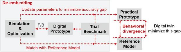
Figure 1 A digital twin model to improve system performance in the real world.
In this paper, the digital twin enables high-fidelity modeling of the RF front end by embedding measurement-driven data into the design. That is, the design leverages S-parameter measurements, simulation feedback, and hardware characterization to build a closed-loop calibration model. This allows for predictive optimization of the RF-SIC filter response, aligning realistic information from signal propagation paths and interconnects. In particular, referring to Fig. 2, the digital twin supports:
• Precision modeling of the antenna-coupled and filter-coupled paths using measured scattering parameters,
• Dynamic compensation for component-induced phase and amplitude deviations via de-embedding,
• Iterative refinement of the filter parameters and architecture using updated transmission matrices derived from empirical data.
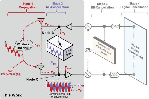
Figure 2 IBFD radio schematic with self-interference cancellation circuitry.
Through a virtual-to-physical convergence, the digital twin model enables proactive tuning of the cancellation circuitry before fabrication. By doing so, there is significant improvement in matching the simulated measured system behavior. This approach not only enhances cancellation accuracy across a wide bandwidth, but also reduces the design cycle time and cost.
In this paper, we implemented the digital twin concept in developing an antenna plus filter package to enhance RF performance. The digital twin framework implemented herewith is feedback-driven to ensure that component mismatches are accurately represented and compensated for. By closely integrating measurements with virtual modeling, a robust and scalable RF cancellation strategy suitable for next-generation IBFD systems is achieved.
The computational implementation of the digital twin framework is straightforward and practical. The T-matrix cascade for interconnecting components involves multiplications of complex matrices. This operation is completed in milliseconds on standard computing hardware. Each component’s S-parameters are measured once using a calibrated vector network analyzer (VNA), and the resulting T-matrices are cascaded to compute the equivalent mismatch matrix as defined in (4.2).
The filter optimization uses a Genetic Algorithm (GA) with a population of 100 individuals and a maximum of 500 generations for global search, followed by a Gradient Descent algorithm for local refinement. Notably, the combined optimization converges in approximately 10–15 minutes on a standard laptop across the 1 GHz operating bandwidth. The digital twin model is then updated on-demand. This is done whenever: 1) a physical component is replaced or re-characterized, 2) its measured S-parameters are updated in the cascade, and when the filter design is redone. In the current implementation, two to three such iterations were sufficient to achieve the target isolation level.
An important practical concern was a potential divergence between the digital twin model and the physical hardware. This arises from unaccounted parasitic effects or measurement noise.
After each fabrication cycle, the measured combined isolation is compared against the de-embedded filter target prediction (Fig. 7). If a significant discrepancy is observed, the process is iterated and the affected components are re-measured, the T-matrix cascade is updated, and the filter design is refined. This measurement-grounded iterative loop ensures that the digital twin remains anchored to physical reality and prevents unchecked model drift.
3 TWO-STAGE CANCELLATION IN IBFD RADIOS
A typical IBFD radio is depicted in Fig 2. The first two stages of this multi-stage SIC begin with the antenna (Stage 1), followed by the RF filter (Stage 2). This paper focuses on designing/combining the first two stages of IBFD radio. Implementing this architecture requires the cancellation of the transmitted signals that leak into the receiver [21]. Past work [7] has shown that a 4-arm spiral antenna can achieve up to 40 dB of isolation using polarization diversity. One pair of this 4-arm spiral is used for transmission, and the other pair is used for reception. The RF-SIC filter behind the spiral provides for additional cancellation of the transmitted leakage signal. As much as 25 to 30 dB of SIC from the RF-SIC filter [22] (Stage 2) is expected. To achieve this, the filter must replicate the leaked antenna-coupled signal into the receiver [10].
To ensure high isolation, it is important to align the phase of the cancellation signal and to concurrently account for component impairments, added cables, and connectors. Due to the very low level of signals being processed, any amplitude and phase mismatches can lead to ineffective cancellation. Figure 3 shows the achievable 2nd stage RF-SIC cancellation with respect to phase and amplitude deviations. As depicted, even a few degrees in phase or a fraction of a dB mismatch between the antenna and cancellation circuitry can cause significant performance variations.
Assuming that the RF-SIC filter response is and the Tx-Rx antenna coupling is (see Fig. 2), the cancellation conditions are satisfied by
| (1) |
Alternatively, (1) can be stated as
and
| (2) |
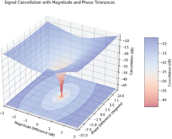
Figure 3 Achievable cancellation in dB as a function of phase and amplitude mismatches.
Furthermore, for the sake of simplicity, we only consider analyzing the self-interference (SI) signal, ignoring the desired one. From Fig. 2, the second stage of signal cancellation occurs at node C. At this node, the coupled signal from node S is weighted (filtered) and used to cancel the incoming leakage SI signal , which indeed is the coupled transmitted signal after antenna stage cancellation. Figure 4 illustrates the first two stages of cancellation, where node S and node C are represented as splitter and combiner respectively. Following Fig. 4, the combined two-stage cancellation, can be represented as
| (3) |
The above equation corresponds to the total achievable cancellation for stages 1 and 2. All the parameters used in (3) are described in Fig. 4. And as noted, fabrication flaws, frequency-dependence, and the presence of parasitic effects in practical components impact the achievable cancellation in practice. To enhance the overall cancellation in the 2nd stage, the next section will describe a de-embedding process. Our goal is to account for any design deviations in the practical components.
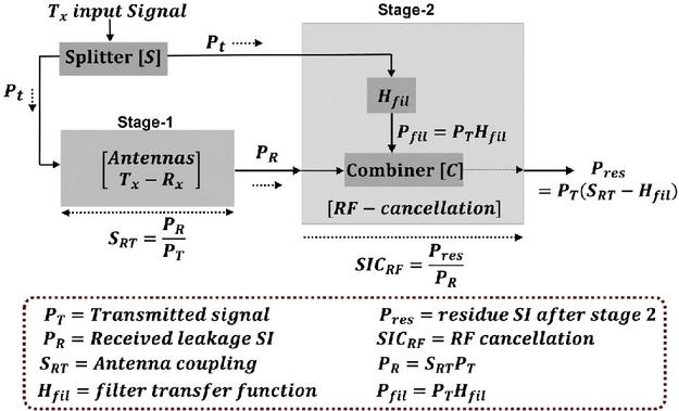
Figure 4 Combined two-stage cancellation.
4 DE-EMBEDDING PROCESS
4.1 Implementing Stage 1 and 2
Past work has shown that a 4-arm spiral antenna (Stage 1) can achieve up to 40 dB of transmit/receive isolation [7]. As usual, the 4-arm spiral used one pair of arms for transmission and the other pair for reception. Subsequently, the RF-SIC filter is used to cancel the leakage that is not canceled in the antenna stage.
Stage 2 is a RF filter constructed with a set of microstrip stubs load cascaded with specific delays to form the RF-SIC filter. Each RF filter stub was terminated with a radial section for broadband operation. Notably, each stub’s impedance and length are key design parameters. Further, we used two attenuators on both sides of the filter to reduce power levels and counteract large signal mismatches. Unlike previous designs [10], our filter leverages the impedance and delay properties of the microstrip stubs, reducing the number of discrete components and avoiding bandwidth limitations. A filter order of 6 (using polynomial fit) achieved a desired 1 GHz bandwidth. Design optimizations led to a 6th order filter that was fabricated. The details of the periodic stub are given in [21]. However, when stages 1 and 2 were combined, even the addition of simple cables, splitters, or connectors between the antenna and the filter resulted in a severe impact in terms of RF cancellation. Below, we discuss a de-embedding approach to overcome the challenge.
4.2 Update filter design using de-embedding
The combined two-stage cancellation architecture (Stages 1 and 2) using practical components is depicted in Fig. 5. As noted, combining the antenna and filter stages requires additional components such as splitters, combiners, cables, connectors, and attenuators. Additionally, connecting cables between the antenna and filter stages introduces further phase delays. Therefore, the filter design must be updated to account for these practical effects.
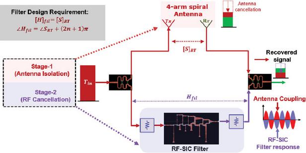
Figure 5 Implementation of IBFD radio using practical components requires de-embedding.
Assuming number of components present in stages 1 and 2 (see Fig. 5), we follow the de-embedding process shown in Fig. 6. To remove component impairments, we convert the corresponding scattering matrix (S-parameters) into a T-matrix for each component, comprising antenna and filter. This T-matrix is also called T-parameters or ABCD-Matrix [23]. This conversion requires measuring the S-parameters of each component and then converting them to the corresponding T-matrices. To do that, the first step involves converting the antenna coupling into a T-matrix (ABCD). can be expressed as
| (4) |
By converting into T-matrix, we have
| (5) |
where . The next step (see Fig. 6) is to take out the effect of combined component impairment. To do that, first we need to estimate the equivalent compensating T-matrix, which corresponds to the total deviations of all practical components from their ideal counterparts. Later, we used its inverse matrix for de-embedding component impairment as follows
| (6) |
where,
Providing the equivalent practical and ideal T-matrices as
Furthermore, following step 4 in Fig. 6 and converting (4.2) back into S-matrix gives as
| (7) |
Using (7), we can update (1) to satisfy the new filter design requirements as
| (8) |
which implies
and
| (9) |
To assess the robustness of the de-embedding procedure, we considered measurement uncertainties through the T-matrix cascade. Each component’s S-parameters were measured using a calibrated VNA with a typical uncertainty of 0.1 dB in magnitude and 1∘ in phase. This was done after SOLT (Short-Open-Load-Through) calibration within the 9.6–10.6 GHz band. For the six cascaded components used in this work (antenna, splitter, two cables, attenuator, and combiner), the root-sum-square (RSS) estimate of cumulative phase uncertainty was approximately 2.5∘. Referring to the sensitivity analysis in Fig. 3, a 2.5∘ phase deviation corresponds to a reduction in achievable RF cancellation of less than 2 dB. This confirms that the de-embedding procedure is robust to address the VNA measurement uncertainty.
A notable advantage of the proposed architecture is that it introduces no additional DC power consumption. This is because the RF-SIC filter, attenuators, splitters, and phase trimmer are all passive components. The primary power-related cost is the insertion loss of the combined filter and coupling network. This insertion loss is approximately 4–6 dB across the 9.6–10.6 GHz operating band. Therefore, it must be accounted for in the overall link budget. It is offset by the significant improvement in receiver isolation achieved through de-embedding. Notably, active RF cancellation approaches achieve similar isolation levels, and typically require several hundred milliwatts of DC power for amplifiers, DACs, and control logic.
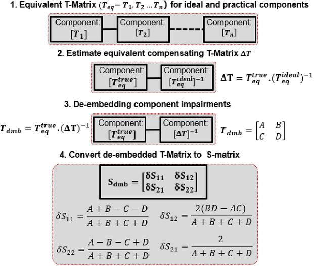
Figure 6 De-embedding ideal vs. practical component mismatch and compensation.
Figure 6 illustrates the de-embedding process to compensate for practical deviations from ideal components. Figure 7 shows the filter design algorithm incorporating de-embedding. This approach restores the expected output by compensating for component impairments in filter design. This strategy ensures accurate modeling and optimization of filter to enhance practical isolation in the RF cancellation stage.
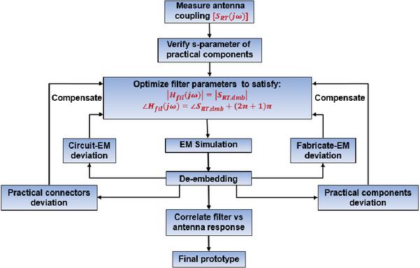
Figure 7 Filter design algorithm.
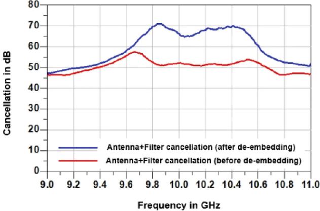
Figure 8 Combined two stages with and without de-embedding.
5 MEASUREMENT RESULTS AND DISCUSSION
The experimental validation was carried out using a calibrated two-port VNA. Prior to full system integration, the S-parameters of each individual component including the SMA cables, broadband splitter/combiner pair, attenuators, and the 4-arm spiral antenna, were measured separately following SOLT calibration at the measurement reference planes. These measured S-parameters were used to populate the T-matrix cascade in the de-embedding process described in section IV. The fabricated 4-arm spiral antenna and RF-SIC filter board (Fig. 9) were stacked vertically and connected using phase-matched cables. Combined isolation measurements ( from Tx port to Rx port), were taken across the 9.0–11.0 GHz range, with the target band being 9.6–10.6 GHz. All measurements were performed under controlled bench conditions to minimize parasitic reflections.
To illustrate the effectiveness of the combined two-stage isolation of the IBFD front end, we conducted measurements of combined antenna and filter cancellation both before and after de-embedding. As seen in Fig. 9, a phase trimmer was used to compensate for phase impairments to enhance isolation. As shown in Fig. 8, the combined isolation is initially constrained within 50 dB due to the effects of non-ideal components. However, after de-embedding and taking out the effect in filter design, combined isolation was increased up to 65 dB across 1 GHz bandwidth, as depicted in Fig. 8. Using de-embedding, a significant improvement of 10–20 dB of isolation can be seen in Fig. 10 across the entire 1 GHz bandwidth from 9.6 GHz to 10.6 GHz.
To better understand the physical mechanism behind the isolation improvement, it is important to trace the source of degradation before de-embedding. When stages 1 and 2 are combined using practical components, each element introduces a small but non-trivial phase delay with amplitude modification that deviates from its idealized model. These individual deviations accumulate across the full signal chain, resulting in a composite phase and amplitude mismatch between the RF-SIC filter output and the antenna-coupled leakage signal arriving at the combiner node (Node C in Fig. 2). As illustrated in Fig. 3, even a 3–5∘ phase error can reduce achievable cancellation by 10 dB or more.
Before de-embedding, the RF-SIC filter was designed to satisfy the ideal condition , without accounting for the intervening practical components. As a result, the combined system isolation was constrained to approximately 50 dB across the 1 GHz band (Fig. 8).
The de-embedding process corrects this by: (1) individually measuring the S-parameters of each component in the chain; (2) converting them to T-matrices and computing the overall equivalent mismatch matrix (from 4.2); and (3) deriving an updated filter design target that incorporates the inverse of . When the RF-SIC filter is redesigned to satisfy , the filter response at the combiner node is effectively pre-distorted to cancel the adverse effects of all practical components. The result is a 10–20 dB improvement in isolation across the entire 1 GHz band. This is a direct consequence of restoring phase and amplitude alignment at the combiner node after accounting for all hardware impairments.
This demonstration can verify that careful consideration of hardware impairments and the effectiveness of the de-embedding process can enhance overall IBFD performance.
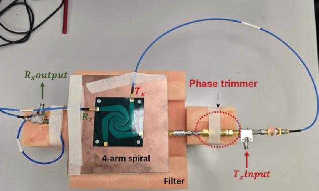
Figure 9 Fabricated IBFD antenna and filter prototype.
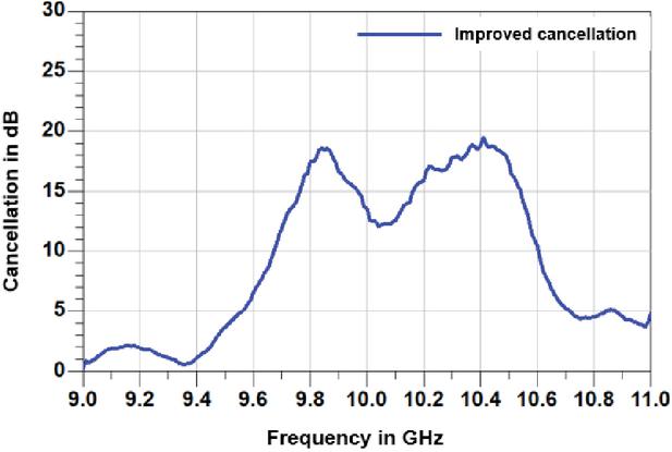
Figure 10 Improved isolation after de-embedding.
Table 1 compares the proposed digital twin-assisted de-embedding approach against a representative set of recently published IBFD and STAR system implementations. Among passive microstrip designs, prior works have demonstrated bandwidths ranging from 20 MHz to 520 MHz, with combined isolation levels of 25–50 dB. The proposed approach achieves a combined isolation exceeding 65 dB across a contiguous 1 GHz bandwidth in the X-band, representing a 10–20 dB improvement over the best comparable passive implementations. Unlike active or mixed-signal approaches that require digital converters or external tuning hardware, our architecture relies entirely on passive components characterized through the digital twin-assisted de-embedding workflow. This is a cost-effective and scalable method, and is directly applicable to next-generation IBFD radio platforms.
Table 1 Comparison of performance with existing state-of-the-art STAR/IBFD system implementations
| Ref. | Technology/Design | Bandwidth | Isolation | Circuit | Stages | Process |
| [8] | Antenna + Resonator | 520 MHz | 30 dB | Passive | 1 | Microstrip |
| [5] | Multi-tap delay line | 200 MHz | 45 dB | Active | 1 | Switch cap. |
| [11] | Antenna + SIC Filter | 500 MHz | 44 dB | Passive | 2 | Microstrip |
| [24] | LNA + EBD | 500 MHz | 44 dB | Passive | 2 | Microstrip |
| [18] | Photonic mixers | 1 GHz | 28 dB | Photonic | 2 | Photonic |
| [25] | Co-polarized antenna | 100 MHz | 25 dB | Passive | 1 | MS (defected gnd.) |
| [26] | Antenna + circulator | 400 MHz | 40 dB | Active | 2 | Microstrip |
| [27] | Hybrid metamaterial-TL | 500 MHz | 39 dB | Active | 1 | Microstrip |
| [12] | Tapped delay line | 120 MHz | 50 dB | Passive | 2 | Microstrip |
| [28] | Cavity-like structure | 400 MHz | 43 dB | Passive | 1 | Cavity slot |
| [29] | Co-horiz. pol. antennas | 520 MHz | 37 dB | Passive | 1 | Multi-layer MS |
| [30] | Dual polarized + rat race | 280 MHz | 50 dB | Active | 2 | Microstrip |
| [31] | Dual polarized antenna | 100 MHz | 47 dB | Passive | 1 | Microstrip |
| [15] | Multi-tap SIC | 20 MHz | 30 dB | Passive | 1 | Microstrip |
| *This Work | DT-Assisted RF-SIC + 4-arm Spiral | 1 GHz | 65 dB | Passive | 2 | Microstrip |
| *DT = Digital Twin; MS = Microstrip; EBD = Electrical Balance Duplexer. | ||||||
The proposed digital twin-assisted de-embedding framework offers several practical advantages. First, it is entirely passive and requires no active components, ADCs, or tuning circuits, making it inherently low-cost and power-efficient. Second, the methodology is modular. That is, each component is individually characterized from standard VNA measurements, making it straightforward to apply to new hardware configurations. Third, the iterative closed-loop structure allows the digital twin to be refined as prototypes are fabricated, reducing design cycle time.
The primary applications of this work include: (1) next-generation 5G/6G base stations requiring simultaneous transmit and receive over wide bandwidths; (2) cognitive radio architectures exploiting IBFD for dynamic spectrum access; (3) radar-communications co-existence systems where transmitter-receiver isolation is critical; and (4) tactical military communication systems requiring compact, passive, wideband IBFD front ends.
In closing, it is important to note some limitations. The de-embedding procedure is hardware-specific. That is, when a physical component is replaced or the system topology changes, re-characterization and filter re-optimization are required. The achievable isolation is also bounded by the accuracy of the phase trimmer and the SNR of the VNA measurement setup. Furthermore, in highly dynamic wireless channels where the self-interference channel may vary rapidly, this passive approach may require supplemental digital cancellation at the baseband stage.
6 CONCLUSION
Our study presents a novel de-embedding approach to enhance the isolation in broadband IBFD radios through a strategic combination of advanced antenna design and RF-SIC filter realization. The successful implementation of our digital-twin aided de-embedding strategy not only enhances isolation but also ensures the robust performance of IBFD systems across a wide bandwidth in the X-band. Our proven de-embedding method increased cancellation by up to 15 dB on average across the whole 1 GHz bandwidth, reaching a maximum of 65 dB when the first two stages were combined. This work paves the way for more efficient and low-cost IBFD radio designs in future communications systems.
Looking ahead, several directions merit further investigation. First, the digital twin framework given here can be extended to reconfigurable and electronically tunable RF-SIC filter architectures, enabling real-time adaptation to changes in hardware state or operating frequency. Second, integration of the proposed analog-domain cancellation with subsequent baseband and digital cancellation stages (Stages 3 and 4 in Fig. 2) would allow a full-system evaluation of the combined isolation chain. Third, the de-embedding methodology is not limited to the X-band and can be applied to sub-6 GHz and mmWave IBFD systems with appropriate component characterization. Finally, further study into automated, sensor-embedded digital twin calibration for tracking component drift with near real-time compensation represents a promising avenue toward fully self-calibrating IBFD radios.
ACKNOWLEDGMENT
This work was partially funded by NSF IUCRC, NSF SWIFT, and NSF ENG-ADVWIRE:CCSS under the grant numbers 2052764, 2128628, and 2430828, respectively.
REFERENCES
[1] G. R. B. Injila, “In band full duplex (IBFD) technology for next generation wireless networks: A survey in cellular networks,” China Communications, vol. 20, no. 5, pp. 20–39, 2023.
[2] M. R. Rahman, S. Bojja Venkatakrishnan, T. Nakatani, and J. L. Volakis, “Wideband Self Interference Cancellation (SIC) RF front end for Simultaneous Transmit and Receive (STAR) radios,” in 2022 IEEE International Symposium on Antennas and Propagation and USNC-URSI Radio Science Meeting (AP-S/URSI), pp. 948–949, 2022.
[3] M. R. Rahman, S. Bojja-Venkatakrishnan, and J. L. Volakis, “Ultra-wideband RF Self interference cancellation filter for STAR radios,” in 2021 IEEE International Symposium on Antennas and Propagation and USNC-URSI Radio Science Meeting (APS/URSI), pp. 523–524, 2021.
[4] K. E. Kolodziej, B. T. Perry, and J. S. Herd, “In-band full-duplex technology: Techniques and systems survey,” IEEE Transactions on Microwave Theory and Techniques, vol. 67, no. 7, pp. 3025–3041, 2019.
[5] C. W. Morgenstern, Y. Rong, A. Herschfelt, A. C. Molnar, A. B. Apsel, D. G. Landon, and D. W. Bliss, “Analog-domain self-interference cancellation for practical multi-tap full-duplex system: Theory, modeling, and algorithm,” IEEE Journal on Selected Areas in Communications, vol. 41, no. 9, pp. 2796–2807, 2023.
[6] B. Debaillie, D.-J. van den Broek, C. Lavín, B. van Liempd, E. A. M. Klumperink, C. Palacios, J. Craninckx, B. Nauta, and A. Pärssinen, “Analog/RF solutions enabling compact full-duplex radios,” IEEE Journal on Selected Areas in Communications, vol. 32, no. 9, pp. 1662–1673, 2014.
[7] A. Hovsepian, E. A. Alwan, and J. L. Volakis, “A wideband, scanning array of four-arm spiral elements for simultaneous transmit and receive,” IEEE Antennas and Wireless Propagation Letters, vol. 19, no. 4, pp. 537–541, 2020.
[8] X.-K. Zhang, Y.-H. Ke, X.-Y. Wang, S.-C. Tang, and J.-X. Chen, “Broadband dual-polarized dielectric patch antenna with high isolation for full-duplex communication,” IEEE Antennas and Wireless Propagation Letters, vol. 22, no. 4, pp. 878–882, 2023.
[9] K. J. Tang, L. H. Ye, W. J. Zhu, J.-F. Li, and D.-L. Wu, “Broadband dual-polarized magnetoelectric dipole antenna for in-band full-duplex application,” IEEE Antennas and Wireless Propagation Letters, vol. 22, no. 9, pp. 2210–2214, 2023.
[10] S. Bojja Venkatakrishnan, E. A. Alwan, and J. L. Volakis, “Wideband RF self-interference cancellation circuit for phased array simultaneous transmit and receive systems,” IEEE Access, vol. 6, pp. 3425–3432, 2018.
[11] M. N. A. Tarek and E. A. Alwan, “Wideband, low profile coupling suppression circuit for simultaneous transmit and receive system based on hybrid finite impulse response and resonator topology,” IEEE Access, vol. 10, pp. 126508–126515, 2022.
[12] K. E. Kolodziej, J. G. McMichael, and B. T. Perry, “Multitap RF canceller for in-band full-duplex wireless communications,” IEEE Transactions on Wireless Communications, vol. 15, no. 6, pp. 4321–4334, 2016.
[13] H. Li, J. Van Kerrebrouck, O. Caytan, H. Rogier, J. Bauwelinck, P. Demeester, and G. Torfs, “Self-interference cancellation enabling high-throughput short-reach wireless full-duplex communication,” IEEE Transactions on Wireless Communications, vol. 17, no. 10, pp. 6475–6486, 2018.
[14] A. Kiayani, M. Z. Waheed, L. Anttila, M. Abdelaziz, D. Korpi, V. Syrjälä, M. Kosunen, K. Stadius, J. Ryynänen, and M. Valkama, “Adaptive nonlinear RF cancellation for improved isolation in simultaneous transmit–receive systems,” IEEE Transactions on Microwave Theory and Techniques, vol. 66, no. 5, pp. 2299–2312, 2018.
[15] Y. Liu, X. Quan, W. Pan, and Y. Tang, “Digitally assisted analog interference cancellation for in-band full-duplex radios,” IEEE Communications Letters, vol. 21, no. 5, pp. 1079–1082, 2017.
[16] X. Yu, J. Ye, L. Yan, T. Zhou, X. Zou, and W. Pan, “Photonic-assisted multipath self-interference cancellation for wideband MIMO radio-over-fiber transmission,” Journal of Lightwave Technology, vol. 40, no. 2, pp. 462–469, 2022.
[17] Y. Xing, S. Li, X. Xue, and X. Zheng, “Photonic-assisted RF self-interference cancellation based on optical spectrum processing,” Journal of Lightwave Technology, vol. 40, no. 7, pp. 2015–2022, 2022.
[18] X. Hu, D. Zhu, S. Liu, H. Xiao, and S. Pan, “Photonics-assisted simultaneous RF channelization and self-interference cancellation,” Journal of Lightwave Technology, vol. 41, no. 18, pp. 5902–5910, 2023.
[19] C. W. Morgenstern, Y. Rong, A. Herschfelt, A. C. Molnar, A. B. Apsel, D. G. Landon, and D. W. Bliss, “Analog-domain self-interference cancellation for practical multi-tap full-duplex system: Theory, modeling, and algorithm,” IEEE Journal on Selected Areas in Communications, vol. 41, no. 9, pp. 2796–2807, 2023.
[20] B. R. Barricelli, E. Casiraghi, and D. Fogli, “A survey on digital twin: Definitions, characteristics, applications, and design implications,” IEEE Access, vol. 7, pp. 167653–167671, 2019.
[21] M. R. Rahman, S. Bojja-Venkatakrishnan, and J. L. Volakis, “Miniature footprint of multi-stage self interference cancellation in a STAR radio,” in 2023 IEEE International Symposium on Antennas and Propagation and USNC-URSI Radio Science Meeting (USNC-URSI), pp. 77–78, 2023.
[22] M. R. Rahman, S. Bojja-Venkatakrishnan, M. Pulugurtha, and J. L. Volakis, “Miniaturization of RF SIC filter on high-K ceramic substrate for STAR application,” in 2024 United States National Committee of URSI National Radio Science Meeting (USNC-URSI NRSM), p. 105, 2024.
[23] D. M. Pozar, Microwave Engineering, 3rd ed. Hoboken, NJ: Wiley, 2005.
[24] J.-T. Lim, H.-W. Choi, J.-H. Song, and C.-Y. Kim, “An in-band full-duplex low noise amplifier integrated with an electrical balance duplexer without explicit matching,” IEEE Microwave and Wireless Technology Letters, vol. 33, no. 8, pp. 1175–1178, 2023.
[25] M. Abedian, M. Khalily, P. Xiao, F. Wang, R. Tafazolli, and A. A. Kishk, “MM-wave high isolated dual polarized dielectric resonator antenna for in-band full-duplex systems,” IEEE Access, vol. 11, pp. 38218–38225, 2023.
[26] M. N. A. Tarek, M. R. Guerra, A. Nunez, M. N. Uddin, and E. A. Alwan, “Improving isolation in monostatic simultaneous transmit and receive systems using a quasi-symmetrical self-interference cancellation architecture,” IEEE Journal of Microwaves, vol. 3, no. 2, pp. 655–664, 2023.
[27] K. Y. Yang, W. J. Zhu, L. H. Ye, J.-F. Li, and D.-L. Wu, “Metamaterial-based low-profile broadband in-band full-duplex antenna,” IEEE Antennas and Wireless Propagation Letters, vol. 22, no. 8, pp. 1942–1946, 2023.
[28] C. J. Ma, S. Y. Zheng, and Y. M. Pan, “Millimeter-wave co-polarized in-band full-duplex antenna based on a mode superposition method,” IEEE Transactions on Antennas and Propagation, vol. 71, no. 6, pp. 4675–4685, 2023.
[29] D. Wu, Y.-X. Sun, R. Lian, B. Xiao, M. Li, and K.-D. Xu, “Metasurface antenna with cocircularly polarized radiation characteristics for wideband monostatic simultaneous transmit and receive applications,” IEEE Transactions on Antennas and Propagation, vol. 71, no. 4, pp. 3304–3313, 2023.
[30] Y.-N. Chen, C. Ding, H. Zhu, and Y. Liu, “A 45∘-polarized antenna system with four isolated channels for In-Band Full-Duplex (IBFD),” IEEE Transactions on Antennas and Propagation, vol. 71, no. 4, pp. 3000–3010, 2023.
[31] Q. Tan and K.-M. Luk, “Wideband co-linearly polarized magneto-electric dipole antenna for in-band full-duplex applications,” IEEE Transactions on Antennas and Propagation, vol. 71, no. 2, pp. 1907–1912, 2023.
BIOGRAPHIES

Md Rakibur Rahman (Member, IEEE) received his Bachelor’s and Master’s degrees in Applied Physics, Electronics, and Communication Engineering from the University of Dhaka, Bangladesh, in 2010 and 2012, respectively. From 2012 to 2017, he worked as a telecommunications engineer in Bangladesh. He later pursued a second Master’s degree (2022) and a Ph.D. (2024) in Electrical Engineering at Florida International University (FIU), Miami, FL, USA. Following his Ph.D., he worked as a Postdoctoral Associate at the RFCOM Lab at FIU until April 2025. He is currently working as a Wireless Systems Engineer at Apple. Since 2018, his research has focused on developing simultaneous transmit and receive (STAR) radio and secure wireless communication links. His research interests include spectral-efficient radio communication, in-band full-duplex radio (IBFD), interference mitigation in wireless links, ultra-wideband wireless communication, software-defined radio (SDR), high-speed wireless communication system benchmarks, RF transceiver design, and the modeling and design of high-performance RF components using advanced circuit-EM simulation tools.

Satheesh Bojja Venkatakrishnan (Senior Member, IEEE) was born in Tiruchirappalli, India, in 1987. He received the bachelor’s degree in electronics and communication engineering from the National Institute of Technology Tiruchirappalli, in 2009, and the M.S. and Ph.D. degrees in electrical engineering from The Ohio State University (OSU), Columbus, OH, USA, in 2017. He was a Scientist at DRDO, India, from 2009 to 2013, working on the development and implementation of active electronic steerable antennas. He is currently a Research Assistant Professor of electrical and computer engineering at Florida International University. His current research interests include receiver design for communication circuits, RF systems, and digital signal processing using FPGAs. He is also working on simultaneous transmit and receive systems (STAR), to improve the spectral efficiency. He has been a Phi Kappa Phi Member, since 2015, and is also an Associate Member of USNC–URSI. He was a recipient of the IEEE Electromagnetic Theory Symposium (EMTS2019) Young Scientist Award. He won the 2nd prize in International Union of Radio Science General Assembly and Scientific Symposium (URSI-GASS) Student Paper Competition held at Montreal, Canada, in August 2017. He also received the Honorable Mention in the Student Paper Competition at the IEEE Antenna and Propagation Symposium (AP-S/URSI), in 2015 and 2016, and the Student Fellowship Travel Grant Award at the U.S. National Committee for the International Union of Radio Science (USNC–URSI), in 2016 and 2017.

John L. Volakis (S’77-M’82-SM’89-F96) obtained his B.E. Degree, summa cum laude, in 1978 from Youngstown State Univ., Youngstown, Ohio, M.Sc. in 1979 from The Ohio State Univ., Columbus, Ohio and the Ph.D. degree in 1982, also from the Ohio State Univ.
Prof. Volakis started his career at Rockwell International North American Aircraft Operations (1982–84), now Boeing. In 1984, he was appointed Assistant Professor at the University of Michigan, Ann Arbor, MI, becoming a full Professor in 1994. He also served as the Director of the Radiation Laboratory from 1998 to 2000. From January 2003 to Aug. 2017 he was the Roy and Lois Chope Chair Professor of Engineering at the Ohio State University, Columbus, Ohio and served as the Director of the ElectroScience Laboratory from 2003 to 2016. From 2017–2023 he was the Dean of the College of Engineering and Computing. Since 2023, he is a Professor in the Electrical and Computer Engineering at Florida International University (FIU).
Over the years, he carried out research in computational methods, antennas, wireless communications and propagation, electromagnetic compatibility and interference, design optimization, RF materials, multi-physics engineering, millimeter waves, terahertz and medical sensing. His publications include 9 books, over 450 journal papers and 950 conference papers, 33 book chapters and 32 patents/disclosures. Among his co-authored books are: Approximate Boundary Conditions in Electromagnetics, 1995; Finite Element Methods for Electromagnetics, 1998; 4th and 5th ed. Antenna Engineering Handbook, 2007 and 2019; Small Antennas, 2010; Integral Equation Methods for Electromagnetics, 2011; and Wearable Antennas and Electronics, Artech House, 2022. He has graduated/mentored over 100 doctoral students/post-docs with 44 of them receiving best paper awards at conferences. His service to Professional Societies include: 2004 President of the IEEE Antennas and Propagation Society (2004), Chair of USNC/URSI Commission B (2015–2017), Chair and Vice Chair of the International Radio Science Union (URSI) Commission B (2017–23), twice the general Chair of the IEEE Antennas and Propagation Symposium, IEEE APS Distinguished Lecturer, IEEE APS Fellows Committee Chair, IEEE-wide Fellows committee member & Associate Editor of several journals. He was listed by ISI among the top 250 most referenced authors (2004). Among his awards are: The Univ. of Michigan College of Engineering Research Excellence award (1993), Scott award from The Ohio State Univ. College of Engineering for Outstanding Academic Achievement (2011), IEEE AP Society C-T. Tai Teaching Excellence award (2011), IEEE Henning Mentoring award (2013), IEEE Antennas & Propagation Distinguished Achievement award (2014), The Ohio State University Distinguished Scholar Award (2016), The Ohio State Univ. ElectroScience Lab. George Sinclair Award (2017), URSI Booker Gold Medal (2020), Advanced Computational Electromagnetics Society Fellow, American Association for the Advancement of Science Fellow, and National Academy of Inventors Fellow (2021).
ACES JOURNAL, Vol. 41, No. 7, 603–613
DOI: 10.13052/2026.ACES.J.410701
© 2026 River Publishers