A Low Cost, Wideband, Microstrip Patch Antenna Array With Improved Gain for Millimeter-Wave Applications
Zakir Khan1, 2, Ce Zhang2, Saeed Ur Rahman3, Xiao-Chuan Wang1, 2, Lei Wen1, 2, and Wen-Zhong Lu1, 2
1School of Optical and Electronic Information and Key Lab of Functional Materials for Electronic Information Huazhong University of Science and Technology, Wuhan 430074, China
zakirkhan@mail.ustc.edu.cn, wxc@hust.edu.cn, wenlei@mail.hust.edu.cn, lwz@hust.edu.cn
2Advanced Manufacturing Institute Huazhong University of Science and Technology, Wenzhou 325035, China
zhangce@wzhust.com,
3School of Electronic Engineering Xidian University, China
saeed@xidian.edu.cn
Submitted On: June 26, 2025 Accepted On: October 14, 2025
Abstract
In this paper the design and analysis of a low cost, wideband and high gain 22 elements patch antenna array for millimeter-wave (mmWave) applications is presented. The proposed antenna array has been designed and fabricated using the cost-effective F4B substrate which is an economical and a suitable option for high frequency communication applications. The final geometry of the unit cell contains a slotted octagonal ring on the outside and a small parasitic octagonal ring on the inner side, connected by crossed-shape strip lines. A prototype of the proposed antenna element and array has been fabricated, which demonstrates a good agreement between the simulated and measured results. According to 10 dB matching bandwidth criteria, the proposed antenna array operates at frequency range 23.8–29.0 GHz, achieving a maximum gain of approximately 13.5 dBi and efficiency range 83–91% at its operating frequencies. The high performance of the proposed antenna array compared to the existing designs along with its simple design and cost-effectiveness demonstrate its potential for high data rate mmWave wireless communication applications.
Keywords: Bandwidth, efficiency, fifth-generation, millimeter-wave, parasitic patch, wideband..
1 INTRODUCTION
In recent years, the lifestyle of the world has been significantly changing due to the development of wireless communication systems, most specifically in the past two decades. The increased demands for high data rates have demonstrated that ubiquitous communication systems are required to support the rising demand for high data rates. In response, substantial work has been done in the development of next generations, specifically fifth-generation (5G) communication standards. In 5G and upcoming wireless communication, the role of the millimeter-wave (mmWave) band is really important due to providing gigabit per second (Gbps) data throughput capability, enhanced user capacity and unprecedented bandwidth [1, 2, 3]. This technology offers various important features that can improve connectivity and performance of communication systems including high data rates in ultra-HD video streaming, low latency in real time applications such as self-driving cars and robotic surgeries, and the ability to support a large number of devices for Internet of Things (IoT) applications in smart cities. Limited bandwidth of the sub-6 GHz band, which is already crowded by current wireless standards, motivated researchers to utilize the spectrum in mmWave bands [4, 5]. Along with various advantages of mmWave communication, there are some disadvantages, i.e., multipath fading and attenuation are very eminent due to poor refraction and diffraction effects [6, 7], which is exacerbated by environmental factors such as rain and foliage. Therefore, along with a wide impedance bandwidth, a high gain directive antenna system is required for both mobile terminals and base stations to overcome high path losses and support potential wireless applications.
The deployment of high-performance antenna arrays is a promising solution to deliver high data rate and maintain reliable connectivity for future wireless communication. Various types of antenna arrays can be used for mmWave applications, which includes multi-layered printed circuit board (PCB) antennas such as magnetoelectric (ME) dipoles by [8], tightly coupled dipole antenna (TCDA) by [9, 10] and tapered slot Vivaldi antennas by [11]. However, these antennas have complex profiles, multilayers and expensive fabrication processes. Therefore, microstrip patch antennas are the widely used solution due to its compact form and simple design geometry which makes them perfectly suited for modern wireless applications.
Few mmWave antennas have been designed [12, 13, 14, 15, 16, 17], however, these designs face limitations such as narrow bandwidth, bulky size, low efficiency or high cost due to complex design and fabrication process. In [12], a 65 element array having a size of 10196.5 mm2 fed by proximity couple has been designed. While this antenna achieves a high gain of 21 dBi, the operating bandwidth is narrow at 27.5–28.5 GHz, and it has a larger size and complex design geometry. In [13], a mmWave antenna array measuring 7063.52.2 mm3 utilizing substrate integrated waveguide (SIW) feeding has been designed. The antenna operates over a frequency range 27.4–28.94 GHz, providing a bandwidth of 1.54 GHz and a gain of approximately 13.5 dBi. However, the design has a bulky size and complex geometry with four layers, and SIW feeding is used making it difficult and costly to fabricate. Similarly, a dual band patch antenna array for 5G applications has been designed in [14, 15]. The designed antennas have compact sizes and achieve gain of 13.5 dBi; however, it exhibits limitations in achieving a broad bandwidth and utilizes Rogers RT5880, which is costly for fabrication.
A planar antenna array having a dimension of 66150.3 mm3 for 5G communication has been designed in [16]. The antenna array operates at 24–29.5 GHz and achieves a gain of 12 dBi, while it consists of a complex design geometry having substrate integrated cavity (SIC) which makes the fabrication difficult and costly. The authors in [17] proposed an inset feed antenna array having size of 10017.45 mm2 for 5G communication. The design operates at frequency range 24.35–31.13 GHz, provides a broadband of 6.7 GHz and a gain of 19.88 dBi, however, the design geometry consists of multiple layers of substrate which make the fabrication difficult and increases the cost for desired applications.
To address these challenges, a high-performance mmWave antenna array is required, characterized by low cost, broad bandwidth, compact size, better integration capability and high gain, which aims to overcome the limitations of existing state-of-the-art designs and minimize issues related to attenuation and potential path loss in the mmWave band. Therefore, this work proposes an octagonal ring patch antenna array, which is mainly focused on the enhancement of bandwidth for high data rates applications, high directivity and efficiency to overcome the losses in mmWave communication and simplifying the design complexity and cost-effectiveness by utilizing a low-cost substrate F4B, which is economical and efficient when compared to expensive Rogers RT5880, and using a single layer to minimize fabrication cost, with future plans to advance beamforming and beam scanning functionalities.
The rest of the paper is organized as follows. Section 2 presents the detailed methodology and geometry of the proposed antenna array. Section 3 presents various results. Section 4 provides a comparison with related works, and section 5 concludes the paper.
2 MATERIALS AND METHODS
In this section the theoretical detail, methodology and evolution of the proposed antenna array from a circular disc will be discussed in detail.
2.1 Proposed antenna element
The proposed antenna element is shown in Fig. 1 (a) and its prototype in Fig. 1 (b). The overall size of the proposed antenna is 2220 mm2 and its thickness is 0.25 mm. The proposed antenna is single layer and its geometry consists of a patch which is its main radiating element, a substrate and a ground plane. The proposed antenna is printed on one side of a cost-effective substrate., i.e., F4B which has a dielectric constant of and loss tangent tan . The radiating element of the antenna comprises of two octagonal rings coupled through a crossed strip line, with a full ground plane at its bottom layer. The radiating element is fed by a 50 microstrip line, where the inner part of the SubMiniature version-A (SMA) connector is used to feed the microstrip line and the outer part is soldiered to the ground plane. The designing, simulation and mathematical analysis of the proposed antenna has been carried out in a commercially available computer simulation technology (CST) Microwave studio software [18].
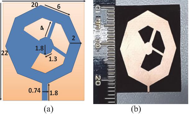
Figure 1 Proposed designed antenna: (a) geometry and (b) prototype.
2.2 Design evolution
The primary design of the proposed antenna is an octagonal shaped patch extracted from a circular disc having 8 mm radius as shown in Figs. 2 (a) and 2 (b). The resonating frequency of a circular patch can be calculated by (1) [19] as:
| (1) |
where is resonating frequency, X for TM11 dominant mode, ae effective radius of the circular patch, C free space light speed and is substrate relative permittivity.
To calculate ae of the circular patch, (2) is used [19]:
| (2) |
Equation (2) is used to design an octagonal patch by relating the area of octagonal and circular patch given in (3):
| (3) |
The side length of the octagonal patch is found to be 6 mm. The primary design gives us a very narrow bandwidth. Therefore, various types of techniques in the form of etching a slot, inserting a parasitic patch, and direct-coupled strip-lines, shown in Figs. 3 (a) and 3 (b), will be applied to obtain a wide impedance bandwidth.
Etching a slot in the conductive patch causes a significant change in current distribution and introduces multiple resonant modes that are overlapped with the fundamental resonance and results in the broadening of the impedance bandwidth. In the next step, a parasitic patch is inserted which is placed inside the main patch that shift the characteristic modes to the desired resonant frequencies by capacitive loading of the parasitic patch which facilitate coupling effects that further optimize the bandwidth [20]. Finally, the direct coupled strip lines connecting the two patches result in better impedance matching and broad bandwidth. These techniques couple the parasitic patch to the main radiating element which produces double resonance by the driven patch and parasitic patch which results in bandwidth enhancement of the proposed antenna element [21]. Using these techniques has enhanced bandwidth in the state-of-the-art designs [22, 23]. Furthermore, a parametric study of antenna dimensions was also performed to optimize antenna dimensions. The wide bandwidth was improved by analyzing the current distribution and precise positions of the parasitic patch, slots length and cross-shaped strip line. S11 comparison of the various designs is illustrated in Fig. 3 (c).
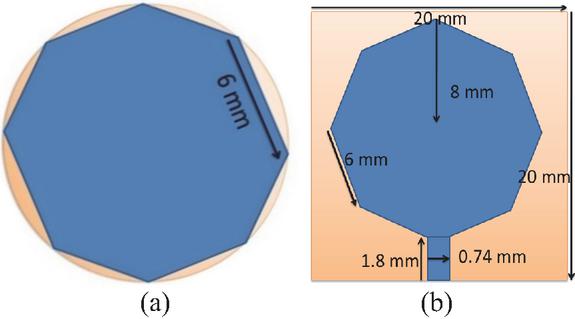
Figure 2 Extracting octagonal patch: (a) octagonal patch and (b) primary octagonal patch antenna.
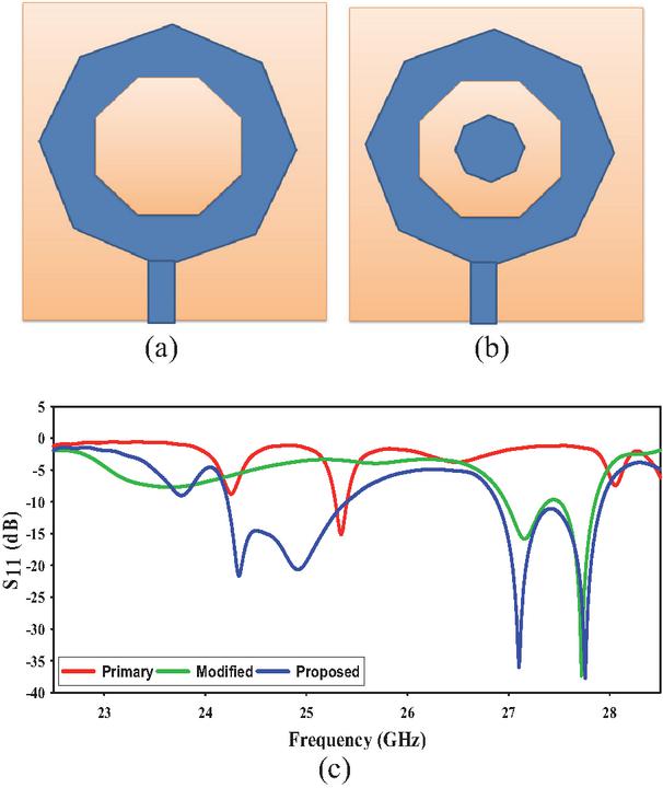
Figure 3 Antenna design evolution: (a) primary design, (b) modified design, and (c) S11 comparison.
2.3 Detailed geometry of the antenna array
Multipath fading and attenuation at mmWave band is very eminent due to poor refraction and diffraction effects. Therefore, a high gain advanced antenna system is required for both mobile terminals and base station to overcome these high path losses and to support potential wireless applications. Before designing an array, we need to design a proper feeding network that works as a power splitter to excite each element of the array.
A series-parallel sequential feeding power splitter has been designed and simulated without the attachment of the antenna elements. To connect the antenna element with each terminal of the feedline, a three-step quarter-wave impedance matching transmission line has been used. For matching to a 50 (port 1) feed line, we need to match the other branching strips of the feeding network to the input impedance by equations (4) and (5) [24]:
| (4) |
where N number of branching points, Z0 initial input impedance:
| (5) |
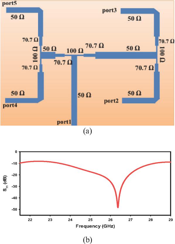
Figure 4 Feeding network of proposed antenna array: (a) geometry of feed-line and (b) S11 of feed-line.
As shown in Fig. 4 (a), the 50 feed line is given in the start as an input to port 1 which is connected to 100 two parallel lines. These 100 are further matched to another 100 with the help of a 70.71 quarter wave impedance transformer and, further, they are connected to ports 2 to 5. The performance of the feedline is analyzed. From the S11 graph, it is perceived that the feeding network is well matched and, according to 10 dB impedance matching, the feeding network is resonating at frequency range 23.0 to 29.0 GHz. The return loss graph of the feeding network is illustrated in Fig. 4 (b), where maximum matching is around 50 dB at 26.5 GHz.
The detailed geometry and prototype of the proposed 22 elements array is illustrated in Figs. 5 (a) and 5 (b). The total dimensions of the antenna array is 50500.25 mm3. The separation distance between the elements of antenna array can be usually kept as () to decrease mutual coupling and prevent grating lobes [19]. The overall geometry of the array comprises of (22) elements, which have element spacing of 0.6 between the two elements along horizontal direction Dx, and 0.55 spacing along the vertical direction Dy.
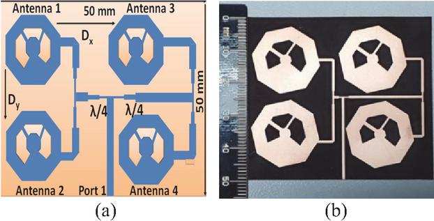
Figure 5 Proposed antenna array: (a) geometry and (b) prototype front.
3 RESULTS AND DISCUSSION
Various results of the proposed final antenna array are discussed in this section.
3.1 Return loss
The ratio of the incident power to the power reflected is termed as the return loss and is expressed in dB, which is used to observe how much energy is transmitted to the radiator by the input power through the transmission line. The S11 value should be less than 10 dB for an efficient antenna to perform well. A 2.92 (D360B50H01-118) SMA was used at the input feeding port of the proposed antenna to measure S11. First, calibration of the VNA is performed with different types of open, short and load connectors and then measurement of the return loss over a specific frequency is performed. From the measurement results, the proposed antenna element is dual-band operating at frequency range 23.8–25.1 GHz and 26.75–27.9 GHz. Similarly, it is observed that the array bandwidth is further enhanced as compared to a single element due to the phenomena of a mutual coupling [25] feeding network. Measured results show that the antenna array is operating in the frequency range 23.8–29.0 GHz. The simulated and measured results of S11 are illustrated in Figs. 6 (a) and 6 (b), which demonstrate good agreement, however the small deviation might be due to environmental factors, measurement setup and manually soldering of the SMA connector. The measurement setup is shown in Fig. 6 (c).
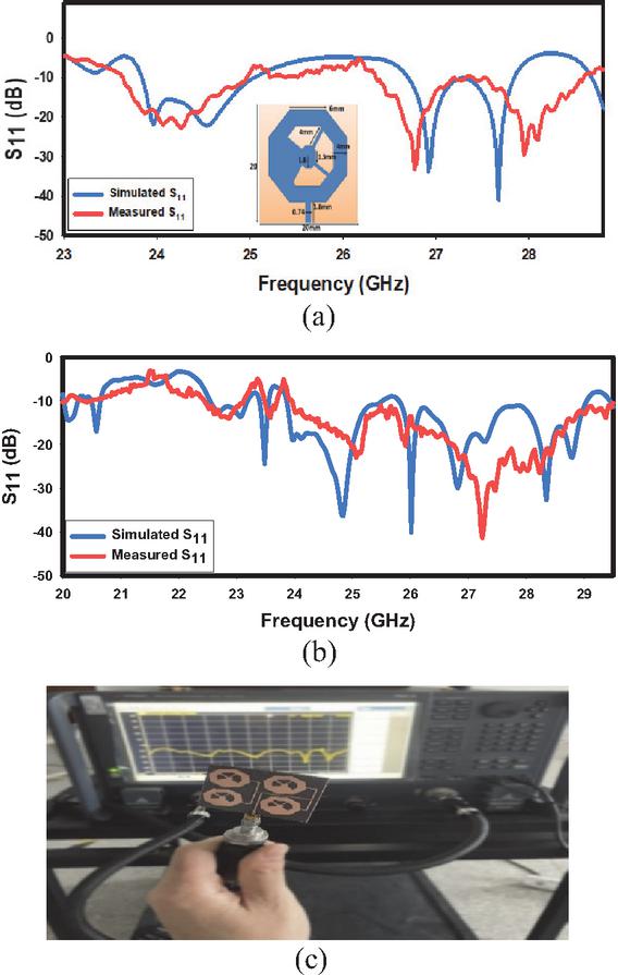
Figure 6 S11 parameter of antenna: (a) return loss of single antenna, (b) return loss of array and (c) measurement setup.
3.2 Radiation pattern
The measure of the maximum energy of the antenna in a specified direction is its radiation pattern. The radiation pattern of the proposed array has been analyzed and measured in an anechoic chamber at 25 GHz and 27.5 GHz which is shown in the two-dimensional (2D) pattern in Figs. 7 (a) and 7 (b) and in the three-dimensional (3D) pattern in Figs. 7 (c) and 7 (d). It can be seen that the simulated and measured results agree with each other, however there is a minor discrepancy which might be due to factors such as measurement setup limitations, environmental factors and manually soldiering of the SMA connector. The array gives a broadside pattern with main lobe direction at around 0–10 degree. Moreover, the array pattern is directive, giving a high directivity of about 14 dBi at 25 GHz and 13.5 dBi at 27.5 GHz, which can be used for numerous mmWave wireless communication applications.
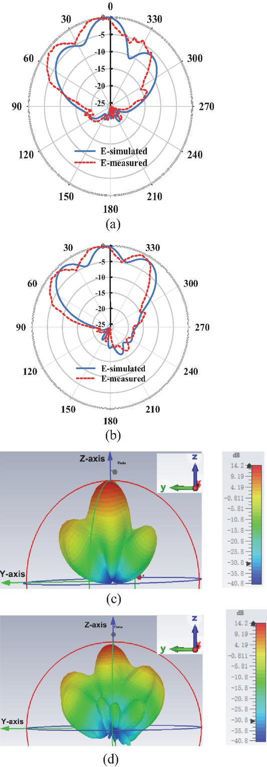
Figure 7 Simulated and measured radiation pattern: (a) 2D pattern at 25 GHz, (b) 2D pattern at 27.5 GHz, (c) 3D pattern at 25 GHz and (d) 3D pattern at 27.5 GHz.
3.3 Gain
The simulated and measured gain versus frequency of the proposed antenna array is represented in Fig. 8. The antenna gain has been measured in an anechoic chamber where a calibrated horn antenna is used at a specific distance as a reference antenna, the proposed antenna is antenna under test (AUT) and the gain is calculated by a specific formula. The array gain has been improved due to high numbers of antenna elements. The proposed antenna array gives high gain of 13.5 dBi at 26 GHz and 12.5 dBi at 28 GHz.
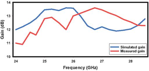
Figure 8 Gain versus frequency plot of the proposed antenna.
3.4 Efficiency
A graph of total and radiated efficiency versus frequency of the proposed antenna array is illustrated in Fig. 9. The array gives a very high efficiency and its radiated and total efficiency is 83–91% at its operating frequencies.
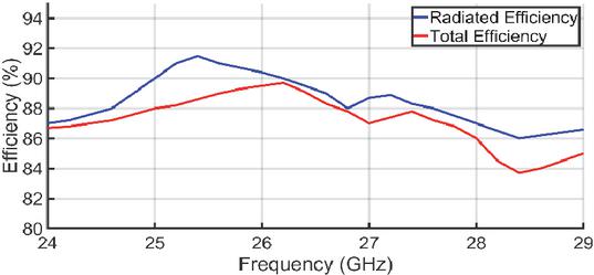
Figure 9 Total and radiated efficiency of the antenna array.
Table 1 Comparison of proposed antenna array with state-of-the-art
| S | NL | Size () | Eff (%) | BW | G | Sub | Ref |
| 1 | 2 | 8.918.490.04 | – | 1 | 21 | Taconic TLY-5 | [12] |
| 2 | 4 | 6.42 5.83 0.20 | 60–78 | 1.5 | 13 | Rogers 4350 | [13] |
| 4 | 1 | 2.93 0.67 0.065 | 85.6 | 1.3 | 13.5 | Rogers 5880 | [14] |
| 5 | 1 | 2.38 1.590.04 | 92 | 0.4 | 12 | Rogers 5880 | [15] |
| 6 | 2 | 5.28 1.2.03 | 90 | 5.5 | 11.5 | – | [16] |
| 3 | 2 | 8.13 1.42 0.11 | 75–86 | 6.7 | 18 | Rogers 5880 | [17] |
| 7 | 1 | 3.97 3.97 0.02 | 83–91 | 5.2 | 13.5 | F4B | This Work |
| S serial number, NL number of layers, Eff efficiency, BW bandwidth, G gain, Sub substrate. | |||||||
4 COMPARISON WITH STATE-OF-THE-ART
The proposed antenna array has been compared with existing designs in Table 1. Notably, the proposed antenna array demonstrates better performance as compared to the existing designs mentioned in the state-of-the-art. The proposed array has a more compact size than the designs in [12, 13, 16, 17]. Additionally, the impedance bandwidth of the proposed antenna array is better than [12, 13, 14, 15]. While the designs in [16, 17] exhibit better broad bandwidth, they contain a more complex geometry design containing multiple layers. The gain of the proposed antenna array is better than [14, 16, 17, 18]. Furthermore, the proposed array is single layer and fabrication cost is minimized by utilizing a cost-effective substrate and standard PCB fabrication technique compared to more complex multi-layer and high-cost designs. Based on performance, the proposed antenna array is a good option which can be used for numerous mmWave wireless communication applications.
5 CONCLUSION
In this paper, a single layer, low cost, wideband, high gain antenna element and antenna array operating at 28 GHz have been proposed for mmWave applications. The innovative techniques of the proposed design have resulted in a significant improvement in high-performance results over the existing designs in the state-of-the-art, without requiring a complex design and multilayer configuration. The proposed array has been fabricated and the measured results show close resemblance with the simulated results. The high-performance results of the proposed antenna, resonating at frequency range 23.8–29 GHz achieving a wide bandwidth up to 5.2 GHz, a high gain of about 13.5 dBi and efficiency 83–91% make it an ideal candidate for numerous mmWave wireless communication applications.
ACKNOWLEDGMENT
This research work was supported by Wenzhou City Key Technology Development Funding ZG2023033.
REFERENCES
[1] J. Qiao, X. S. Shen, J. W. Mark, Q. Shen, Y. He, and L. Lei, “Enabling device-to-device communications in millimeter-wave 5G cellular networks,” IEEE Communications Magazine, vol. 53, no. 1, pp. 209–215, 2015.
[2] M. Stanley, Y. Huang, T. Loh, Q. Xu, H. Wang, and H. Zhou, “A high gain steerable millimeter-wave antenna array for 5G smartphone applications,” in 11th European Conference on Antennas and Propagation (EUCAP), pp. 1311–1314, 2017.
[3] T. S. Rappaport, Y. Xing, G. R. MacCartney, A. F. Molisch, E. Mellios, and J. Zhang, “Overview of millimeter-wave communications for fifth-generation wireless networks: With a focus on propagation models,” IEEE Transactions on Antennas and Propagation, vol. 65, no. 12, pp. 6213–6230, 2017.
[4] R. M. Nelson, D. A. Rogers, and A. G. D’Assuncao, “Resonant frequency of a rectangular microstrip patch on several uniaxial substrates,” IEEE Transactions on Antennas and Propagation, vol. 38, no. 7, pp. 973–981, 1990.
[5] H. Gutton and G. Baissinot, “Flat aerial for ultra-high frequencies,” French Patent, vol. 703113, 1955.
[6] W. Hong, K.-H. Baek, Y. Lee, Y. Kim, and S.-T. Ko, “Study and prototyping of practically large-scale mmWave antenna systems for 5G cellular devices,” IEEE Communications Magazine, vol. 52, no. 9, pp. 63–69, 2014.
[7] H. Zhou, “Phased array for millimeter-wave mobile handset,” in 2014 IEEE Antennas and Propagation Society International Symposium (APSURSI), pp. 933–934, 2014.
[8] Y. Li and K.-M. Luk, “A 60-GHz wideband circularly polarized aperture coupled magneto-electric dipole antenna array,” IEEE Trans. Antennas Propag., vol. 64, no. 4, pp. 1325–1333, Apr. 2016.
[9] J. A. Kasemodel, C.-C. Chen, and J. L. Volakis, “Broadband planar widescan array employing tightly coupled elements & integrated balun,” in Proc. IEEE Int. Symp. Phased Array Syst., pp. 467–472, Oct. 2010.
[10] Z. Khan, C. Zhang, M. Zhang, X. Wang, W. Lu, and W. Lei, “An integrated feed ultrawideband Tightly-Coupled Dipole Antenna (TCDA) array for mmWave 5G communication systems,” in IEEE 12th Asia-Pacific Conference on Antennas and Propagation (APCAP), pp. 1–2, 2024.
[11] T. Logan, R. W. Kindt, and M. N. Vouvakis, “Low cross-polarization Vivaldi arrays,” IEEE Transactions on Antennas and Propagation, vol. 66, no. 4, pp. 1827–1837, 2018.
[12] H. A. Diawuo and Y.-B. Jung, “Broadband proximity-coupled microstrip planar antenna array for 5G cellular applications,” IEEE Antennas and Wireless Propagation Letters, vol. 17, no. 7, pp. 1286–1290, 2018.
[13] S.-J. Park and S.-O. Park, “LHCP and RHCP substrate integrated waveguide antenna arrays for millimeter-wave applications,” IEEE Antennas and Wireless Propagation Letters, vol. 16, pp. 601–604, 2016.
[14] M. I. Khattak, A. Sohail, U. Khan, Z. Barki, and G. Witjaksono, “Elliptical slot circular patch antenna array with dual band behaviour for future 5G mobile communication networks,” Progress in Electromagnetics Research C, vol. 89, pp. 133–147, 2019.
[15] J. Khan, D. A. Sehrai, and U. Ali, “Design of dual band 5G antenna array with SAR analysis for future mobile handsets,” Journal of Electrical Engineering & Technology, vol. 14, no. 2, pp. 809–816, 2019.
[16] C.-X. Mao, M. Khalily, P. Xiao, T. W. Brown, and S. Gao, “Planar sub-millimeter-wave array antenna with enhanced gain and reduced sidelobes for 5G broadcast applications,” IEEE Transactions on Antennas and Propagation, vol. 67, no. 1, pp. 160–168, 2018
[17] M. Khalily, R. Tafazolli, P. Xiao, and A. A. Kishk, “Broadband mmWave microstrip array antenna with improved radiation characteristics for different 5G applications,” IEEE Transactions on Antennas and Propagation, vol. 66, no. 9, pp. 4641–4647, 2018.
[18] SIMULIA. CST Studio Suite ® [Online]. Available: https://www.cst.com.
[19] K. F. Lee, K. M. Luk, and H. W. Lai, Microstrip Patch Antennas. Singapore: World Scientific, 2017.
[20] G. Kim and S. Kim, “Design and analysis of dual polarized broadband microstrip patch antenna for 5G mmWave antenna module on FR4 substrate,” IEEE Access, vol. 9, pp. 64306–64316, 2021.
[21] G. Kumar and K. P. Ray, Broadband Microstrip Antennas. Norwood, MA: Artech House, 2003.
[22] N.-W. Liu, L. Zhu, W.-W. Choi, and X. Zhang, “A low-profile aperture-coupled microstrip antenna with enhanced bandwidth under dual resonance,” IEEE Transactions on Antennas and Propagation, vol. 65, no. 3, pp. 1055–1062, 2017.
[23] Z. Khan, M. H. Memon, S. U. Rahman, M. Sajjad, F. Lin, and L. Sun, “A single-fed multiband antenna for WLAN and 5G applications,” Sensors, vol. 20, no. 21, p. 6332, 2020.
[24] J. D. Kraus and R. J. Marhefka, Antennas: For All Applications. New Delhi: Tata McGraw-Hill Publishing Company Ltd., 2001.
[25] W. Yang, K. Ma, K. S. Yeo, and W. M. Lim, “A compact high-performance patch antenna array for 60-GHz applications,” IEEE Antennas and Wireless Propagation Letters, vol. 15, pp. 313–316, 2015.
BIOGRAPHIES

Zakir Khan received the B.Sc. Engineering degree in Telecommunication Engineering from the University of Engineering and Technology (UET), Peshawar, Pakistan, in 2013, the master’s degree in Electrical Engineering from COMSATS University, Abbottabad, in 2016, and the Ph.D. (Engineering) degree from the University of Science and Technology of China (USTC) in 2022 in Electronic Science and Technology. He was with the University of Naples, Parthenope, Italy, 2022–2024. Currently, he is a postdoctoral researcher at Advanced Manufacturing Institute of HUST in Wenzhou, China. His major research interests include microwave/mmWave antenna design and microwave remote sensing.

Ce Zhang (S’11–M’16) received the B.E. degree in electronic communication engineering from the City University of Hong Kong, Hong Kong, in 2011, and the Ph.D. degree in electrical engineering from the University of Washington, Seattle, WA, USA, in 2016. He worked at Tubis Technology (now Kyocera) from 2016 to 2017, Amazon Inc. from 2017 to 2019 and Facebook (now Meta) from 2019 to 2023. From 2023 to now, he works at Huazhong University Advanced Manufacturing Research Institute. His current research interests include antenna design, phased array system, and signal processing and electromagnetic theory in wireless power transfer and radar imaging system.

Saeed ur Rahman completed his B.S. degree from COMSATS University Abbottabad, Pakistan, and his master’s degree from Capital University of Science and Technology (CUST), with a major in Electronic Engineering. He completed his Ph.D. degree from Nanjing University of Aeronautics and Astronautics, Nanjing, China, majoring in Information and Communication Engineering. He worked as a postdoctoral fellow from 2020 to 2022 at Nanjing University of Aeronautics and Astronautics, Nanjing. He has been working as an associate professor at Xidian University, Xi’an, since 2022. His major research includes electromagnetic and microwave technology, especially in meta surfaces, antennas, and intelligent reflective surfaces (RIS).

Xiao-Chuan Wang (M’ 14) received the B.E. degree in electronic science and technology and the Ph.D. degree in microelectronics and solid-state electronics from the Huazhong University of Science and Technology, Wuhan, China, in 2005 and 2010, respectively. From 2010 to 2015, he served as a Lecturer with the Department of Electronic Science and Technology, Huazhong University of Science and Technology, where he was promoted to Professor within the School of Optical and Electronic Information in 2023. His current research interests include microwave and millimeter-wave components.

Lei Wen is a Professor and Ph.D. supervisor at the School of Optical and Electronic Information in Huazhong University of Science and Technology (HUST), and vice dean of Advanced Manufacturing Institute of HUST, Wenzhou, China. He obtained his Ph.D. degree in Materials Science at HUST in 2008. His research activities are mainly concerned with microwave dielectric materials and components for microwave communication. He has undertaken more than 30 research projects supported by the National Natural Science Funds, the National Key Research and Development Program of China, and about 200 academic papers have been published and several research productions have been applied successfully for antennas, resonators and LTCC modules.

Wen-Zhong Lu received the Ph.D. degree in electronic materials and components from Huazhong University of Science and Technology, Wuhan, China, in 1994. From 1997 to 1998, he was a Research Scholar with the Department of Physics, Moscow University, Moscow, Russia. In 2002, he was a Senior Research Scholar in Material Research Center. Manchester University, Manchester, UK. He is currently a Professor and Dean of Advanced Manufacturing Institute of Huazhong University of Science and Technology in Wenzhou. He has authored or coauthored more than 300 journal and conference papers. His current research interests include microwave functional materials and components.
ACES JOURNAL, Vol. 40, No. 10, 1037–1044
DOI: 10.13052/2025.ACES.J.401009
© 2025 River Publishers