A 3 dB Coupler With Defected Ground Structure for Feeds Applied to High-Power Intelligent Metasurface
Weidong Kong1, 2, Jinyu Wang1, Shixiong Deng2, Qiaonan Wang1, 2, Leiqiang Ma4, Biao Zhou2, Xuefeng Song2, Kuang Zhang1, Guohui Yang1, Yang Li3, and Cong Wang1
1School of Electronic & Information Engineering
Harbin Institute of Technology, Harbin 150001, China
23b905073@stu.hit.edu.cn, jinyuwang@stu.hit.edu.cn, wangqn8678@163.com, zhangkuang@hit.edu.cn, gh.yang@hit.edu.cn, kevinwang@hit.edu.cn
2Hebei Semiconductor Research Institute
Shijiazhuang 050051, China
shixiode@163.com, CZ1314233@163.com, hsri_sxf@163.com
3School of Integrated Circuits
Shandong University, Shandong 250100, China
yang.li@sdu.edu.cn
4Southwest China Research Institute of Electronic Equipment
Chengdu, China
lqma_hit@126.com
Submitted On: July 08, 2025; Accepted On: September 08, 2025
Abstract
This paper proposes a 3 dB coupler with high-power handling capability feeds applied to high-power intelligent metasurface, based on loosely coupled structures and defected ground structure (DGS). The proposed coupler structure consists of two tandem coupled couplers with a coupling coefficient of 8.34 dB and a DGS, a design that significantly enhances the couplers’ ability to handle high power levels. The measurement results are in good agreement with the simulation results: within the 3.5 to 4.5 GHz range, the return loss exceeds 21.4 dB, the isolation is at least 20.8 dB, the insertion loss is less than 0.3 dB, and the phase difference between output ports is 93–94.5∘. Furthermore, the coupler can handle high power exceeding 1.5 kW with a 10% duty cycle. The proposed 3 dB coupler features low insertion loss, high isolation, low return loss, high-power capability, and can improve the power capability of intelligent metasurface systems.
Keywords: 3 dB coupler, defected ground structure (DGS), high power, metasurface..
1 INTRODUCTION
In next-generation communication systems, the application of metasurface will attract significant attention. Compared to traditional phased array beam scanning methods, metasurface-based beam scanning systems rely on a single active amplifier for feeding, thereby imposing higher output power requirements on the amplifier than conventional active phased array beam scanning. To advance the engineering application of metasurface, high-power electromagnetic energy feeding sources will be indispensable, as show in Fig. 1. Therefore, high-power couplers play a critical role in metasurface-based communication systems for power combining [1].
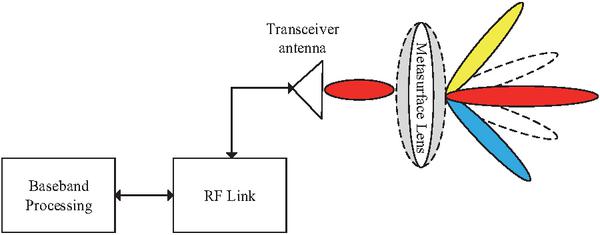
Figure 1 Metasurface beam scanning system.
With the rapid advancement of modern communication systems, miniaturization has become an irreversible trend, driving the transition from traditional discrete components to hybrid integrated circuits (HICs). HICs integrate multiple functional modules into a single package, significantly reducing system size while enhancing performance and reliability [2]. In the radio frequency (RF) domain, couplers are typically constructed using coaxial lines, waveguides, and microstrip lines. Coaxial lines and waveguides exhibit high-power handling capability but are bulky and unsuitable for HICs [3], whereas microstrip couplers are more suitable for HICs due to their compact structure [4]. Conventionally, couplers fabricated by printed circuit board (PCB) suffer from poor heat dissipation, are prone to overheating and line burnout at high power, and have large dimensions [5]. For heat dissipation requirements, thin-film technology on alumina ceramic substrates is an optimal choice: 99.6% pure alumina ceramics with a thermal conductivity of 37 W/(mK) offer advantages of good heat dissipation, low loss, small size, and excellent performance in high-temperature environments [6, 7].
Traditional Lange couplers are difficult to manufacture due to the narrow spacing and width of coupling lines and are prone to arc breakdown at high power [8]. Therefore, the proposed 3 dB coupler employs two tandem connected loose couplers to solve the problem of close coupling line spacing, and a defected ground structure (DGS) is introduced to further increase the coupling line spacing and enhance power handling capability, achieving a high-power handling capability of 1.5 kW. The proposed coupler based on thin-film technology on alumina ceramic substrates features high-power handling capability, low insertion loss, and small size, with measurement results in good agreement with simulations.
2 CIRCUIT ANALYSIS AND DESIGN FOR HIGH POWER
2.1 Structure of the proposed 3 dB coupler
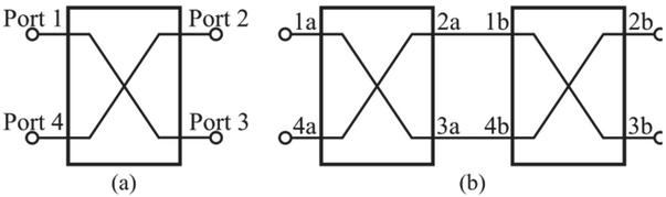
Figure 2 Four-port network. (a) Single coupler and (b) two-stage tandem coupler.
Figure 2 (a) shows a four-port coupler structure. Assume that the signal level of Port 1 is 1, the signal level of Port 4 is 0 and the coupling coefficient is C. Therefore, the signal level of Port 2 is C, and the signal level of Port 3 is [9, 10]. Then the scattering parameter matrix of this coupler can be written:
| (1) |
Two identical couplers are connected in series as shown in Fig. 2 (b), and the signal levels of its two output ports can be calculated from (1):
| (2) | ||
| (3) |
For a 3 dB coupler, both output ports are equal in level amplitude:
| (4) |
The values of C are obtained from (4), (8.34 dB) or 0.9239 (0.69 dB). Therefore, a 3 dB coupler can be composed of tandem two loose couplers, thus increasing the coupling line spacing and power handling capability. A 3 dB coupler, designed by cascading two 8.34 dB couplers, demonstrates the simulated electric field (E-field) distribution shown in Fig. 3, with a 1.5 kW pulse wave at a 10% duty cycle fed into the input port.
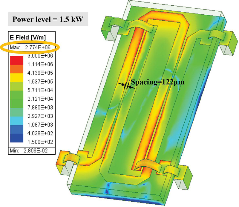
Figure 3 E-field distribution simulation of the 3 dB coupler.
The 3 dB coupler has a coupling line spacing of 122 m. In Fig. 3, the maximum field strength is 2.77106 V/m, which is close to the breakdown field strength of air ( V/m). In practice, the coupler must be designed with a maximum field strength of less than 70% of the ultimate breakdown field strength to ensure stable operation over long periods of time. Therefore, the coupling line spacing needs to be further increased to reduce the maximum field strength.
2.2 Analysis of DGS
From [11, 12], the coupling coefficients of a typical coupler can be calculated as follows:
| (5) |
where , are the even and odd mode impedances, respectively. Further transformations of (5) are given:
| (6) |
Clearly, the coupling coefficient C is increasing with k. The DGS enhances the field coupling between the coupling lines as seen in [13]. The effect of DGS on coupling lines is:
| (7) |
where means with DGS and means without DGS. The result is obtained by substituting equation (7) into equation (6):
| (8) |
where means with DGS and means without DGS. The results indicate that adding DGS below the coupled microstrip lines can improve the coupling effect between them. Therefore, couplers with DGS can achieve 3 dB coupling with wider coupling line spacing to increase power tolerance.
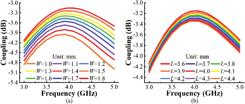
Figure 4 The influence of DGS size on coupling coefficient: (a) when mm and (b) when mm.
To obtain the optimal DGS size, the width and length of the DGS are independently swept for simulation. The effect of DGS size on the coupling coefficient is shown in Fig. 4. The highest coupling coefficient is obtained using a DGS with mm and mm. For microstrip lines, the coupling reduces as the lines separate [14]. Therefore, using a DGS with mm and mm maximizes the coupled line spacing [8]. The proposed 3 dB tandem coupler layout is shown in Fig. 5 with three layers: top metal, alumina ceramic substrate, and bottom metal with DGS. Ultimately, the designed 3 dB coupler has a coupling line spacing of 200 m, which is a 64% increase compared to the coupling line spacing of the coupler without DGS.
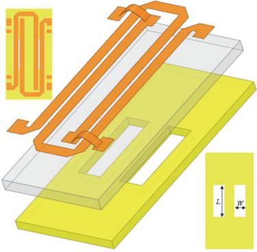
Figure 5 Layout of the 3 dB coupler with DGS.
2.3 Simulation verification for high power
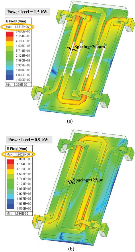
Figure 6 E-field distribution simulation of the 3 dB coupler: (a) with DGS and (b) without DGS.
To validate the effect of DGS on enhancing the coupler’s power handling capability, a 1.5 kW pulse wave with a 10% duty cycle is applied to the input port, and the simulated E-field distribution is shown in Fig. 6 (a). The highest E-field intensity is primarily concentrated between the coupled lines, reaching a value of V/m. For comparison, an E-field distribution simulation was performed for the 3 dB coupler without DGS, with the input power adjusted to achieve the same maximum field intensity as in Fig. 6 (a). The simulation results are shown in Fig. 6 (b). For the 3 dB coupler without DGS, the maximum field strength of 1.96106 V/m was reached when the input power was 0.9 kW. The implementation of DGS effectively improves the power handling capability of the coupler, increasing it by 67% compared to the coupler without DGS, thus meeting the requirements for sustained high-power operation. But DGS may increase fabricating complexity due to sensitivity to dimensional tolerances (as hinted in Fig. 4) and could be less effective at frequencies outside the 3.5–4.5 GHz band due to substrate constraints. Additionally, DGS structures might not scale well to lower frequencies without larger sizes.
The results of the temperature distribution simulation of the proposed coupler are shown in Fig. 7. The ambient temperature is set to 70∘C, using the same input conditions as the E-field simulation. The thermal conductivity of the alumina substrate is set at 37 W/(mK), while that of the top and bottom metallic layers is established at 400 W/(mK). The maximum temperature is 87.6∘C at the coupling line, which is lower than the limiting temperature of the process (260∘C). The above simulation results verify the high-power handling capability of the proposed coupler.
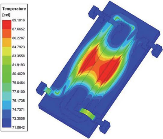
Figure 7 Temperature distribution simulation.
3 FABRICATION AND MEASUREMENT RESULTS
The proposed 3 dB coupler is fabricated by an alumina ceramic substrate with a thickness of 635 m, a purity of 99.6%, and relative dielectric permittivity . Alumina ceramic substrates (99.6% purity) offer a high thermal conductivity of 37 W/(mK). This property is critical for high-power handling, as it efficiently dissipates heat generated during operation, preventing overheating and line burnout, a common issue in PCB-based couplers. The alumina ceramic’s high thermal conductivity directly enhances power handling. This substrate allows for good heat dissipation, low loss, small size, and excellent performance in high-temperature environments. For HICs, alumina ceramics support miniaturization and reliability. Alumina substrates facilitate this through thin-film technology, allowing for compact dimensions and compatibility with high-frequency applications.
Table 1 Comparison with high-power and 3 dB couplers
| Ref. | Technology | Center Frequency (GHz) | Band Width (%) | Power Handling Capability (kW) | Coupling Coefficient (dB) | Through (dB) | Isolation (dB) | Phase Difference (∘) | Size |
| [3] | Coaxial Line | 0.0775 | 187.1 | 2 | 451.3 | 0.65 | 80 | N/A | 0.04 (0) |
| [15] | Coaxial Line | 0.55 | 163.6 | 0.3 | 20 | 0.3 | 40 | N/A | 0.14 (0) |
| [4] | Microstrip (PCB) | 0.44 | 7.8 | 1 | 25 | 0.2 | 66.2 | N/A | 0.040.03 (02) |
| [12] | Microstrip (Al2O3) | 2.5 | 48 | N/A | 4 | 2.5 | 21.4 | 89.2-89.5 | 0.11 (0) |
| [16] | Cross-slot (PCB) | 3.44 | 30 | N/A | 3.59 | 3.39 | 29.18 | 89.1 | 0.190.17 (02) |
| [17] | SISPSL (PCB) | 5 | 16.45 | N/A | 3.70.22 | 3.6060.08 | 15-45 | 900.5 | 0.400.40 (02) |
| This Work | Microstrip (Al2O3) | 4 | 25 | 1.5 | 3.29-3.49 | 3.08-3.3 | 20.8 | 93-94.5 | 0.080.16 (02) |
| SISPSL: Substrate Integrated Suspended Parallel Strip Line. 0 is the wavelength in air at the center frequency. |
The top layer is plated with 2 m of gold using thin-film technology and the bonding wires are 500 25 m gold strips. The design process involved optimizing DGS dimensions to maximize coupling coefficients, Manufacturing tolerances, such as changes in film line width and DGS position alignment, may affect coupling efficiency and field distribution. A 10% tolerance online spacing in thin film processes can alter the maximum electric field strength. The fabricated 3 dB coupler is shown in Fig. 8, with dimensions of mm2, which is well suited to HIC. The detailed physical parameters are (Unit: mm): , , , , .
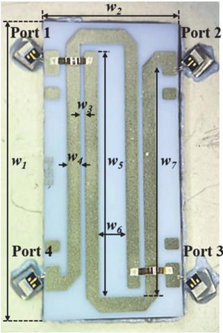
Figure 8 Photograph of the fabricated 3 dB coupler.
Figure 9 shows the small-signal measure results of the fabricated 3 dB coupler. The measured and are 3.29 dB and 3.3 dB at 4 GHz, with good performance. The coupling coefficient is 3.29–3.49 dB, and the insertion loss is less than 0.3 dB, across the frequency range of 3.5 to 4.5 GHz. Return loss and isolation also perform well, greater than 21.4 dB and 20.8 dB, respectively. And (phase difference) is 93–94.5∘ within the operating frequency.
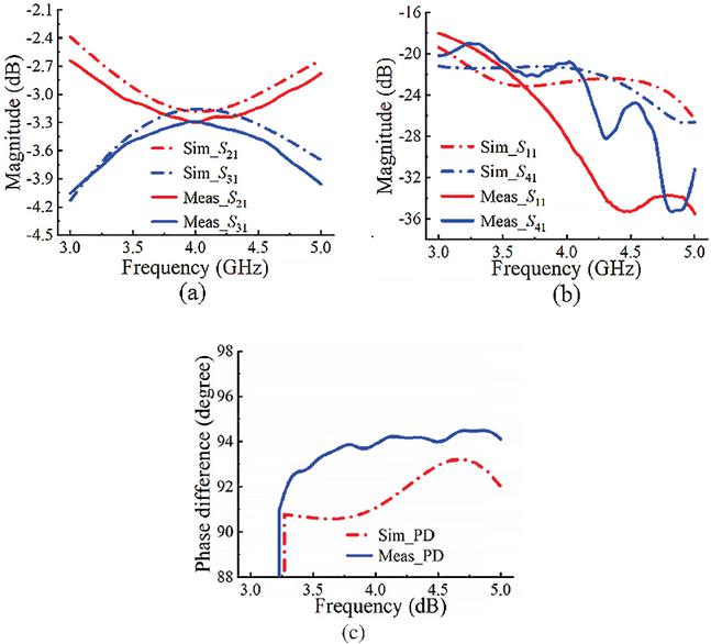
Figure 9 Small-signal simulation and measured results: (a) and , (b) and , and (c) phase difference ().
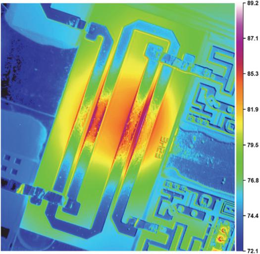
Figure 10 Temperature distribution measured results at high power.
The fabricated coupler was tested for high-power operation and operated continuously for 120 minutes at an input of 1.5 kW with a 10% duty cycle without any abnormalities, with lower duty cycles reducing thermal accumulation and achieving higher peak power tolerance. The duty cycle directly affects thermal management and continuous operation. Our power endurance test ran stably at an ambient temperature of 70∘C and a relative humidity of 40%. Humidity may affect dielectric performance or arc risk. High humidity may lower the air breakdown threshold (currently designed to be below 70% of V/m according to section II.A), affecting long-term reliability. Therefore, it is required to use airtight sealing or substrate coating to ensure low humidity levels. However, arcing occurs when the input power is increased to 2 kW. The results of the high-power temperature test, conducted with a 1.5 kW pulsed wave input and a constant temperature surface maintained at 70∘C at the bottom, are presented in Fig. 10. In agreement with the simulation results, the peak temperature is 89.2∘C at the position of the coupling line, which is less than the tolerable temperature of alumina ceramics. The coupler operates well without any detachment, proving that the coupler can withstand high power exceeding 1.5 kW. Compared with other work, the results are also competitive as shown in Table 1.
4 CONCLUSION
This paper presents a novel 3 dB coupler with a power handling capacity exceeding 1.5 kW. Two innovative solutions are proposed to address the challenge of excessively narrow coupling line spacing: cascading two loosely coupled coupler structures in tandem configuration and introducing a DGS to enhance the coupling coefficient of the transmission lines by 64%. Consequently, the power handling capability is improved by 67% compared to 3 dB couplers without DGS. Comprehensive electromagnetic simulations and experimental measurements validate the excellent performance in terms of S-parameters and high-temperature characteristics. This study can effectively enhance the power handling capacity of metasurface-based communication systems, thereby extending their coverage range.
ACKNOWLEDGMENT
This work was supported in part by the National Natural Science Foundation of China under Grant 62320106002 and Grant U22A2014; in part by the Key Research and Development Program of Shandong Province, China, under Grant 2024KJHZ013; in part by Shandong Provincial Natural Science Foundation of China under Grant ZR2023ZD03.
References
[1] S. Yang, X. Wang, H. Zhu, and G. Lu, “A coupling-path reconfigurable quadrature coupler with wide range of tunable frequencies and power division ratios,” IEEE Transactions on Microwave Theory and Techniques, vol. 72, no. 6, pp. 3530–3541, June 2024.
[2] F. Gardes, A. Shooa, G. De Paoli, I. Skandalos, S. Ilie, T. Rutirawut, W. Talataisong, J. Faneca, V. Vitali, and Y. Hou, “A review of capabilities and scope for hybrid integration offered by silicon-nitride-based photonic integrated circuits,” Sensors, vol. 22, no. 11, p. 4227, 2022.
[3] Z.-B. Wang, X. Wei, H.-P. Fang, H.-M. Zhang, and Y.-R. Zhang, “A compact and broadband directional coupler for high-power radio frequency applications,” IEEE Microwave and Wireless Components Letters, vol. 30, no. 2, pp. 164–166, Feb. 2020.
[4] S.-M. Sohn, A. Gopinath, and J. T. Vaughan, “A compact, high power capable, and tunable high directivity microstrip coupler,” IEEE Transactions on Microwave Theory and Techniques, vol. 64, no. 10, pp. 3217–3223, Oct. 2016.
[5] H.-P. Fang and X. Wei, “Compact directional coupler for high-power applications,” in 2018 12th International Symposium on Antennas, Propagation and EM Theory (ISAPE), Hangzhou, China, pp. 1–3, 2018.
[6] S. Li, L. Zhang, H. Xie, X. Yao, Z. Hao, and H. Dong, “Effect of AlN/Al2O3 thin-film protective layer on the high-temperature performance of ITO thin-film strain gauge,” IEEE Sensors Journal, vol. 23, no. 11, pp. 11490–11497, June 2023.
[7] Z. Zhang, X. Yuan, and L. Xie, “A new package for SiC power modules with ceramic heatsink,” in 2022 IEEE Energy Conversion Congress and Exposition (ECCE), Detroit, MI, USA, pp. 1–7, 2022.
[8] J. Zhang, Z. Wu, F. Xu, and D. Li, “An interdigitated coupler with defect ground structure,” in 2015 IEEE MTT-S International Microwave Workshop Series on Advanced Materials and Processes for RF and THz Applications (IMWS-AMP), Suzhou, China, pp. 1–3, 2015.
[9] H. Hayashi, “Tandem Lange 3-dB 90∘ hybrid implemented on FR4 substrate,” in 2014 NORCHIP, Tampere, Finland, pp. 1–3, 2014.
[10] K. Wincza, K. Staszek, and S. Gruszczynski, “Reduced-length tandem directional couplers composed of coupled-line sections with fixed coupling coefficient,” IEEE Transactions on Microwave Theory and Techniques, vol. 69, no. 3, pp. 1625–1634, Mar. 2021.
[11] M. Abe, Y. Tahara, and N. Yoneda, “A tandem 3-dB hybrid coupler using coupled lines with series capacitance,” in The 40th European Microwave Conference, Paris, France, pp. 164–167, 2010.
[12] R. Behera, K. Sangam, S. S. Lonkadi, A. Andhiwal, K. Singh, and A. V. Nirmal, “Realization of Lange coupler using hybrid technology and its characterization,” in 2022 Trends in Electrical, Electronics, Computer Engineering Conference (TEECCON), Bengaluru, India, pp. 135–141, 2022.
[13] B. Qian, X. Chen, and A. Kishk, “Decoupling of microstrip antennas with defected ground structure using the common/differential mode theory,” IEEE Antennas and Wireless Propagation Letters, vol. 20, no. 5, pp. 828–832, May 2021.
[14] M. Steer, Microwave and RF Design II—Transmission Lines. Raleigh, NC, USA: NC State University, p. 203, 2019.
[15] G. Lin, X. Yin, S. Ren, Z. Wang, Y. Zhi, and T. He, “Compact and broadband directional coupler for high power applications,” Journal of Electromagnetic Waves and Applications, vol. 35, no. 15, pp. 1980–1986, 2021.
[16] K. Abouhssous, L. Wakrim, A. Zugari, and A. Zakriti, “A compact patch coupler using cross-slots for 5G applications,” in 2023 IEEE 3rd International Maghreb Meeting of the Conference on Sciences and Techniques of Automatic Control and Computer Engineering (MI-STA), Benghazi, Libya, pp. 590–594, 2023.
[17] J. Liu, Y. Wang, K. Ma, and W. An, “A differential SISPSL branch-line coupler with common-mode suppression using compensated stub,” IEEE Transactions on Circuits and Systems II: Express Briefs, vol. 70, no. 2, pp. 511–515, Feb. 2023.
Biographies
Weidong Kong received the B.E. and M.E. degrees in Electronics and Information Engineering from Harbin Institute of Technology University, China, in 2014 and 2016, respectively. He is currently pursuing a Doctor of Engineering degree with a specialization in Electronics and Information at Harbin Institute of Technology University.
Jinyu Wang is currently pursuing the M.E. degree at Harbin Institute of Technology, China. His research specializes in microwave power amplifiers and filter design.
Shixiong Deng received the M.E. degree from Beihang University, China, in 2014 and the Ph.D. degree from National University of Defense Technology in 2024. His research focuses on microwave limiters and electromagnetic protection.
Qiaonan Wang received the M.E. degree from the University of Electronic Science and Technology of China. His research interests include microwave voltage-controlled attenuators and microwave filter design.
Leiqiang Ma received the M.E. degree in Electronics and Information Engineering from Harbin Institute of Technology, China, in 2015. His research focuses on microwave receiver module design.
Biao Zhou received the M.E. degree from Hebei Semiconductor Research Institute, China, in 2009. His research interests include microwave active phased array systems.
Xuefeng Song received the M.E. degree from Hebei Semiconductor Research Institute, China. His research specializes in microwave semiconductor chips.
Kuang Zhang (Member, IEEE) received the B.Sc. degree in electronics and information engineering, the M.Eng. degree in electronics engineering, and the Ph.D. degree in communication and information systems from Harbin Institute of Technology (HIT), Harbin, China, in 2005, 2007, and 2011, respectively. He was a Visiting Professor with the University of Wisconsin-Madison, Madison, WI, USA, from 2015 to 2016. Since 2010, he has been with the Department of Microwave Engineering, School of Electronics and Information Engineering, HIT, where he is currently a Professor.
Guohui Yang (Member, IEEE) received the B.S. degree in telecommunication, the M.S. degree in instrument science and technology, and the Ph.D. degree in electromagnetics from the Harbin Institute of Technology, Harbin, China, in 2003, 2006, and 2009, respectively. Since 2009, he has been with the Department of Microwave Engineering, Harbin Institute of Technology, where he is currently an Associate Professor. His current research interests are radio frequency micro electromechanical system (RF MEMS) devices, tunable antennae, frequency selective surface (FSS), electromagnetic compatibility (EMC), and final difference time domain (FDTD).
Yang Li (Senior Member, IEEE) received the Ph.D. degree from the Department of Electronic, Kwangwoon University, Seoul, South Korea, in 2015. He has been a Professor at the School of Microelectronics at Shandong University, Jinan, China, since 2022. His research interests include nanostructured flexible materials, flexible electronics, gas sensors, and memristors.
Cong Wang (Senior Member, IEEE) was born in Qingdao, Shandong, China, in 1982. He received the B.S. degree in automation engineering from Qingdao Technological University, Qingdao, in 2005, and the M.S. and Ph.D. degrees in electronic engineering from Kwangwoon University, Seoul, South Korea, in 2008 and 2011, respectively. Since 2016, he has been with the Department of Microwave Engineering, Harbin Institute of Technology, Harbin, where he is currently a Professor. His major interests include passive device design and fabrication, humidity sensors, and biosensors.
ACES JOURNAL, Vol. 41, No. 2, 155–161
DOI: 10.13052/2026.ACES.J.410206
© 2026 River Publishers