Design and Experimental Validation of a Compact 10 dB Microstrip Directional Coupler for 2.4 GHz Applications
Mehmet O. Kok1, Fatih Kaburcuk2, and Atef Z. Elsherbeni3
1Department of Electrical and Electronics Engineering Nevsehir Haci Bektas Veli University, Nevsehir 50300, Turkey
onurkok@nevsehir.edu.tr
2Department of Electrical and Electronic Engineering Sivas University of Science and Technology, Sivas 58000, Turkey
fkaburcuk@sivas.edu.tr
3Department of Electrical Engineering Colorado School of Mines, Golden 80401, USA
aelsherb@mines.edu
Submitted On: October 22, 2025; Accepted On: January 05, 2026
ABSTRACT
This paper presents the design, simulation, fabrication, and measurement of a compact 10 dB microstrip directional coupler operating at 2.4 GHz and fabricated on a cost-effective FR-4 substrate. The design process integrates analytical even-odd mode impedance synthesis, circuit-level simulation using ADS LineCalc, and full-wave electromagnetic (EM) optimization to control coupling, isolation, and insertion loss with high fidelity. The measured coupling factor was 10.3 dB at 2.4 GHz, with isolation exceeding 18 dB and insertion loss below 0.65 dB. The simulation-to-measurement deviation was only 0.4 dB, indicating strong design-to-fabrication correlation. A reflection coefficient less than 20 dB confirms excellent impedance matching, while the single-layer, compact layout enables easy integration into wireless front ends, antenna feeding networks, and RF measurement systems. Compared with similar FR-4 based couplers in the literature, this proposed design achieves competitive electrical performance and demonstrates better simulation–measurement deviation, without requiring premium substrates, multilayer fabrication, or lumped-element compensation.
Keywords: Coupling factor, directional coupler, wireless communications.
1 INTRODUCTION
Directional couplers are essential passive components in radio-frequency (RF) and microwave engineering, extensively used for monitoring signal power, sampling, and power distribution in wireless communication systems, radar front ends, and measurement instrumentation [1, 2, 3]. These devices enable signal tapping without significant disturbance to the main transmission path, supporting critical functionalities such as antenna feeding, signal routing, and power measurement. Among the numerous directional coupler implementations, microstrip-based designs have gathered significant attention due to their inherently low fabrication cost, planar geometry, and compatibility with standard printed circuit board (PCB) manufacturing processes. This planar form factor also facilitates straightforward integration with other RF front-end components, making microstrip couplers particularly attractive for compact and mass-producible systems. Despite these advantages, microstrip directional couplers inherently face several design challenges that impact their performance metrics such as coupling accuracy, isolation, bandwidth, and reflection coefficient. A fundamental issue lies in the phase velocity mismatch between the even and odd propagation modes of the coupled microstrip lines, which degrades the directivity and isolation of the device [4]. This mode imbalance limits the operational bandwidth and reduces the overall signal fidelity. Additional design complexities arise from the sensitivity of microstrip lines to fabrication tolerances and variations in substrate properties. These factors lead to performance discrepancies between simulated models and fabricated devices, particularly when low-cost substrates such as FR-4 are used.
FR-4 substrates, while widely used due to their affordability and ease of processing, present unique challenges for microwave applications. Their relatively high dielectric loss tangent introduces insertion losses that can compromise signal integrity, and the frequency-dependent dielectric constant introduces dispersion effects that affect phase velocity and impedance matching. Additionally, batch-to-batch variations in FR-4 material properties and inconsistent manufacturing processes further exacerbate performance variability, making accurate prediction and repeatability of directional coupler behavior difficult [5, 6].
Over the past two decades, significant research efforts have pursued to overcome these limitations through innovative design methodologies and novel structural configurations. Phase velocity equalization techniques such as the incorporation of epsilon-negative (ENG) transmission lines [7], fragment-type compensation to balance even/odd modes and raise directivity [8], compact, broadband layouts aimed at high-power handling [9], small-footprint couplers that preserve high directivity [10], application-driven prototypes validated for satellite links [11], and shunt-inductor loading that equalizes phase velocities for systematic directivity enhancement [12]. Other approaches include lumped-element backward couplers [13], tight-coupling fragment-type variants [14], and capacitive compensation using matching networks for wider-bandwidth control [15]. Broader contexts span on-chip lumped couplers [16], asymmetric 2.4 GHz electrical-balance designs [17], and stripline implementations optimized for integration [18]. Additional innovations include calibration techniques enabling accurate incident-power readout in instrumentation [19] and impedance-transforming, high-directivity microstrip couplers [20]. Foundational perspectives derived from composite right/left-handed (CRLH) coupled lines [21] and overlay full-wave analyses [22], together with recent compact broadband branch-line and ultra-compact microstrip realizations [23, 24], define the trade space among bandwidth, directivity, size, and fabrication complexity.
This paper addresses these challenges by presenting a compact, fabrication-tolerant 10 dB microstrip directional coupler operating at 2.4 GHz, implemented entirely on a cost-effective FR-4 substrate. The design methodology integrates a structured computational workflow that combines analytical even–odd mode impedance synthesis, physical dimension extraction via Keysight ADS LineCalc, circuit-level schematic optimization, and full-wave electromagnetic (EM) simulation incorporating realistic fabrication constraints such as conductor thickness, substrate losses, and bending discontinuities. The coupler prototype was fabricated using an LPKF PCB milling machine, with SubMiniature version A (SMA) connectors soldered for measurement purposes. To ensure measurement reliability, all scattering parameter (S-parameter) measurements were performed on a calibrated vector network analyzer using a full two-port SOLT (short–open–load–thru) calibration at the end of the coaxial cables. The measurement uncertainty was estimated to be within 0.05 dB for magnitude and 0.5∘ for phase, based on repeat measurements of the same device under identical test conditions. The measured device exhibits a coupling factor of 10.3 dB and high isolation, closely matching simulation results with a deviation below 0.4 dB, confirming the robustness of the design approach. The compact footprint and low-cost implementation make this design highly suitable for integration in wireless communication front ends, antenna feeding networks, and RF measurement instrumentation.
The proposed 10 dB microstrip directional coupler achieves a simulation–measurement coupling deviation of only 0.4 dB at 2.4 GHz, which is among the lowest reported for FR-4-based designs in the 2–3 GHz range. To substantiate this claim, a systematic literature survey was conducted covering publications from 2010 to 2024 and including only designs fabricated on FR-4 substrates that reported measured S-parameters and a clearly defined operating bandwidth. Designs using alternative substrates, lacking measurement data, or omitting bandwidth specifications were excluded to ensure comparability. Table 1 presents the published results, listing coupling deviation, isolation, reflection coefficient, and bandwidth for each comparable design. While directivity was not directly measured in this work, the measured isolation of 18 dB at the center frequency serves as the primary high-port-separation metric, with further justification provided in section IV. This expanded comparison demonstrates that the proposed coupler combines excellent coupling accuracy with acceptable isolation for WLAN and ISM-band applications, while maintaining a cost-effective single-layer FR-4 implementation that makes it practical for integration into low-cost RF front-end and measurement systems.
2 DESIGN METHODOLOGY
The multi-step design approach combines analytical calculations, circuit simulation, and full-wave EM modeling. This process provides a robust framework for realizing microstrip directional couplers with high fidelity between simulation and practical measurement. The resulting device dimensions are optimized for manufacturability and performance on cost-effective substrates.
2.1 Coupled-line theory and even-odd mode analysis
The directional coupler design is based on coupled microstrip line theory, where two parallel microstrip transmission lines exhibit EM coupling that excites two distinct propagation modes: even and odd. These modes are characterized by different characteristic impedances, denoted as the even-mode impedance () and odd-mode impedance (). The coupling coefficient (C), expressed in decibels (dB), is defined as:
| (1) |
where k is the voltage coupling coefficient. For a symmetric directional coupler referenced to , the even- and odd-mode impedances satisfy the standard relations in (2) and (3). These relations are derived from quasi-static coupled-line analysis and are well established in [25, 26]:
| (2) | |
| (3) |
Equation (1) assumes lossless, quasi-TEM propagation, which is a valid approximation for microstrip lines at low microwave frequencies. The coupling level is directly linked to the difference between and , where larger separation between these impedances yields stronger coupling. For this work, a 10 dB coupling level was targeted at 2.4 GHz, corresponding to the ISM band. To satisfy both the coupling requirement and the matching condition in a 50- system, the selected values were and . These impedances form the theoretical foundation of the design and serve as the input for physical dimension extraction of the coupled microstrip lines. The choice of substrate material plays a principal role in determining both electrical performance and fabrication cost. Here, a widely available FR-4 laminate was employed, characterized by a relative dielectric constant () of 4.4 and a thickness of 60 mils (1.524 mm). Although FR-4 exhibits relatively higher dielectric loss and greater material variability than specialized microwave laminates, its low cost, broad availability, and compatibility with standard PCB fabrication processes make it an appealing choice for many practical RF applications. Accurate knowledge of substrate parameters is critical, as they directly affect the guided wavelength, characteristic impedances, and coupling behavior of the coupled lines. Consequently, substrate properties serve as essential inputs for EM simulation and impedance-to-dimension conversion tools, ensuring that the designed structure achieves the intended specifications when fabricated.
2.2 Microstrip geometry calculation using ADS LineCalc
The transformation from the target even- and odd-mode impedances to the physical dimensions of the coupled microstrip lines requires precise EM modeling that accounts for substrate permittivity, thickness, and conductor geometry. For the present design, the required impedances were and , as derived in section 2.1. These values were selected because they simultaneously achieve the target 10 dB coupling coefficient and satisfy the impedance balance condition for a 50- system, ensuring both proper coupling and port matching.
Using these impedance targets and the specified FR-4 substrate parameters (, thickness 60 mils), Keysight ADS LineCalc was employed to compute the initial physical dimensions of the coupled microstrip lines. The tool applies quasi-static closed-form equations tailored for coupled microstrip structures, enabling rapid and accurate estimation of conductor width () and spacing (). The calculated dimensions were mm and mm.
To ensure robustness of the initial design, these values were cross-validated against classical analytical expressions from the microstrip design literature [1]. This verification confirmed strong consistency between LineCalc outputs and established theoretical models, providing confidence in proceeding to schematic-level simulations and full-wave EM optimization.
2.3 Initial schematic modeling in ADS
Using the calculated physical dimensions, a circuit-level schematic model was developed in Keysight ADS. The coupled-line sections were represented by Microstrip Coupled Lines (MCLIN) elements, which accurately emulate the transmission line behavior based on the specified conductor width (W), spacing (S), and electrical length (L).
Figure 1 shows the circuit schematic of the proposed design. This schematic abstraction enabled rapid evaluation of key performance parameters such as coupling magnitude, port-to-port isolation, reflection coefficients (S11), and phase difference between the coupled output ports. Iterative simulations were performed to fine-tune L of the coupled sections, aiming to achieve an electrical length close to a quarter wavelength at the center frequency of 2.4 GHz. This tuning was critical to optimize the coupling level and ensure proper phase relationships required for the directional coupler to meet its design objectives.
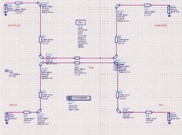
Figure 1 Circuit schematic of the proposed design.
2.4 Full-wave EM simulations
Full-wave EM simulations were conducted in Keysight ADS Momentum to capture physical effects that cannot be resolved through circuit-level analysis. In ADS Momentum, the microstrip lines and substrate are modeled using a Method of Moments (MoM) solver. The solver employs an open-region Green’s function that inherently represents free space, eliminating the need for additional radiation boundary conditions. This approach minimizes unwanted reflections and enables accurate characterization of microstrip behavior, including fringing-field effects. The simulation frequency range was set to 2–3 GHz to encompass the operating band as well as adjacent frequencies relevant to the optimization process. This range ensured stable coupling behavior and supported reliable interpolation during adaptive meshing. Harmonic balance analysis was not required for this design. The complete physical layout, including all bends, tapers, and transmission-line transitions, was exported directly from the schematic to ADS Momentum so that the exact geometry of the coupler was analyzed. Adaptive mesh refinement was applied around edges, bends, and discontinuities where rapid current variations occur, improving accuracy without altering the layout. The simulation setup also considers losses in both the conductor and dielectric materials, based on FR-4 substrate properties such as dielectric constant, loss tangent, and conductor thickness. The fabrication errors are also considered to check how the directional coupler performs in real conditions. This helps to confirm that the simulation results are in good agreement with measurement results.
2.5 Optimization and final tuning
To address discrepancies between the initial schematic model and the full-wave EM simulations, mainly arising from parasitic capacitances, inductances, and higher-order effects, an iterative optimization procedure was applied. The coupled-line length was set to approximately one quarter of the guided wavelength at 2.4 GHz on FR-4 and then trimmed slightly in EM simulations (approximately 17.6 mm) to precisely meet the design frequency. The primary optimization focused on W and S since these directly determine the even- and odd-mode impedances and thus the coupling factor. Fine adjustments were made to W and S around the initial LineCalc estimates of 1.82 mm and 1.20 mm, resulting in mm and mm. In addition, supporting geometrical features were optimized, including the 50- feed-line width, linear taper transitions between feeds and coupled lines, and SMA launch pad dimensions. With these refinements, the optimized design achieved 10 dB coupling at 2.4 GHz, reflection coefficient less than 20 dB, isolation less than 18 dB, and insertion loss approximately 0.65 dB. This process ensured that the final coupler maintains both compact size and robust performance when fabricated on a standard FR-4.
In this work, the fractional bandwidth (FBW) is defined as the frequency range over which the coupler maintains its target performance. Specifically, FBW is taken as the span of frequencies where the coupling remains within 10 0.5 dB, the reflection coefficient is less than 15 dB, and the isolation exceeds 15 dB.
3 SIMULATION AND MEASUREMENT RESULTS
This section provides a comprehensive comparison between the simulated and measured performance of the proposed microstrip directional coupler. The design was rigorously evaluated through both schematic-level circuit simulations and full-wave EM modeling, capturing idealized and realistic EM behaviors respectively. The layout of the proposed design is shown in Fig. 2, and the fabricated prototype is presented in Fig. 3. The prototype was fabricated by PCB milling, equipped with SMA connectors, and characterized by using a calibrated vector network analyzer over the 2–3 GHz range to validate the design and simulation methodology. Measurements employed a two-port SOLT calibration with the reference plane set at the SMA pin interface. All unused ports were terminated with broadband 50 loads.
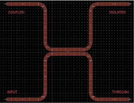
Figure 2 Layout of the proposed design.
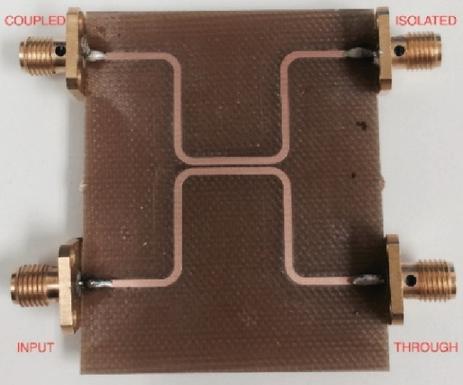
Figure 3 Fabricated prototype of the proposed directional coupler.
The comparison focuses on critical S-parameters, including reflection coefficient (S11), insertion loss (S21), coupling (S31), and isolation (S41) analyzed at the center frequency of 2.4 GHz as well as across the operational bandwidth. The detailed evaluation highlights the close agreement between simulations and measurements, demonstrating the effectiveness of the design process and the suitability of the proposed coupler for practical RF applications.
3.1 Coupling response (S)
The coupling factor at the design frequency of 2.4 GHz is a key performance parameter for the proposed 10 dB directional coupler. As illustrated in the circuit-level schematic results presented in Fig. 4, a coupling value of 10 dB is precisely achieved, matching the design target. Full-wave EM simulations, shown in Fig. 5, revealed a slight deviation, yielding 10.2 dB at 2.4 GHz. This shift is attributed to realistic EM effects, such as parasitic capacitance and fringe-field interactions. Measurement results from the fabricated prototype, presented in Fig. 6, indicated a coupling of 10.3 dB at the center frequency, with only a 0.1 dB difference from the EM simulation, demonstrating close agreement between simulation and measurement and confirming the robustness of the design approach.
3.2 Isolation performance (S)
Isolation at the 2.4 GHz design frequency demonstrated robust performance across all design stages. As shown in the circuit-schematic simulation results (Fig. 4), the predicted isolation exceeded 15 dB, indicating effective suppression of unwanted coupling between the isolated ports. Full-wave EM simulations in Fig. 5 revealed a slight reduction, reflecting the more realistic modeling of parasitic coupling and substrate effects. Measurements of the fabricated prototype in Fig. 6 confirmed an isolation of 18 dB at 2.4 GHz. The reduction relative to the simulations is primarily attributed to fabrication tolerances, connector mismatches, and the inherent material-property variations of FR-4. While some FR-4 designs in the literature report higher isolation, they often achieve this at the expense of larger footprints or multi-layer complexity. Directivity was not measured; therefore, isolation is presented as the primary indicator of high-port separation. Because the reflection coefficient exceeds 20 dB at the center frequency, the measured isolation serves as an indication of expected directivity under these conditions. Overall, the achieved isolation is sufficient for typical WLAN and ISM-band applications.
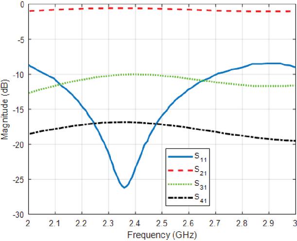
Figure 4 Circuit simulation results of the proposed design.
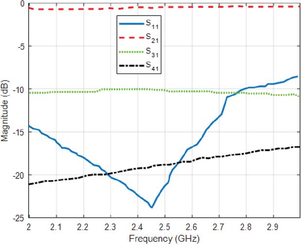
Figure 5 EM simulation results of the proposed design.
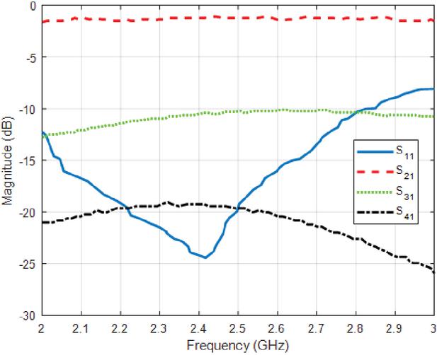
Figure 6 Measured results of the proposed design.
Table 1 Comparison of -10 dB directional couplers fabricated on FR-4 substrates
| Ref. | f0 (GHz) | S (dB) | S (dB) | S (dB) | S (dB) | FBW (%) | (dB) | Size (cm) |
| [3] | 2.45 | 15 | 0.6 | 10 | 18 | 11 | N/A | 3525 |
| [4] | 2.40 | 18 | 0.8 | 10 | 20 | 15 | N/A | 3020 |
| [6] | 2.40 | 16 | 0.7 | 10 | 19 | 13 | 0.7 | 4025 |
| [9] | 2.45 | 17 | 0.7 | 10 | 21 | 10 | 0.4 | 2822 |
| [10] | 2.40 | 18 | 0.9 | 10 | 20 | 12 | 0.6 | 2518 |
| [12] | 2.40 | 15 | 0.9 | 10 | 22 | 14 | 0.8 | 3820 |
| [13] | 2.40 | 16 | 1.0 | 10 | 19 | 12 | 1.0 | 2015 |
| This Work | 2.40 | –20 | –0.65 | –10 | –18 | 13 | 0.4 | 1715 |
3.3 Insertion loss (S) and reflection coefficient (S)
Through-port insertion loss was consistently predicted to be approximately 0.57 dB in both the schematic simulations shown in Fig. 4 and the full-wave EM simulations shown in Fig. 5, indicating effective minimization of conductor and dielectric losses despite the relatively lossy FR-4 substrate. In Fig. 6, measurements of the fabricated prototype show a slightly higher insertion loss of 0.65 dB at 2.4 GHz, an increase of only 0.08 dB compared with the simulations. This minor increase is attributed to additional loss mechanisms, including connector mismatches, soldering imperfections, and small fabrication-induced variations. The reflection coefficient demonstrates strong impedance matching throughout the design process. Measurements confirm this performance, showing reflection coefficient less than 20 dB at the center frequency, indicating excellent input port matching and minimal signal reflection critical for efficient power transfer and low system noise. Based on the FBW definition, the measured FBW of the fabricated prototype is 2.33–2.64 GHz, which corresponds to approximately 13%.
Table 1 compares reported 10 dB directional couplers operating at 2.4 and 2.45 GHz on FR-4 substrates, compiled from the systematic literature survey presented in section I. The proposed design is placed alongside established works to highlight relative strengths and limitations. Earlier contributions [3, 4, 6] demonstrated isolation levels of 18–20 dB with insertion losses of approximately 0.6–0.8 dB, whereas [9, 10] achieved improved isolation of 20–21 dB but required more elaborate geometries. Other approaches, including shunt-inductor loading [12] and lumped-element compensation [13], provided enhanced bandwidth and directivity, albeit with increased design complexity and greater sensitivity to fabrication tolerances. In comparison, the proposed coupler provides a balanced performance, achieving 18 dB isolation and a low insertion loss of 0.65 dB within a straightforward single-layer layout. To the best of the authors’ knowledge, among FR-4 couplers operating at around 2.4 GHz, the design exhibits the smallest reported simulation-to-measurement deviation ( dB), demonstrating strong fabrication tolerance. In addition, its compact core footprint of approximately cm is smaller than many comparable designs. These results indicate that the proposed coupler not only delivers competitive performance but also satisfies practical requirements for cost-effectiveness and ease of fabrication, making it a strong candidate for WLAN and ISM-band.
4 CONCLUSION
This study shows that low-cost FR-4 substrates can deliver performance close to that of premium laminates when accurate electromagnetic modeling is combined with fabrication-aware optimization. A compact 10 dB microstrip directional coupler at 2.4 GHz was designed, simulated, fabricated, and measured using a systematic workflow that included even–odd mode synthesis, circuit-level tuning, and full-wave EM analysis. The measured coupling differed by only 0.4 dB from simulation, confirming high dimensional accuracy and robustness against fabrication and substrate effects. The prototype achieved 18 dB isolation, reflection coefficient less than 20 dB, and insertion loss of 0.65 dB at the center frequency, with quadrature phase balance and a fractional bandwidth of 2.33–2.64 GHz (13%). With its compact size, the design compares well with similar FR-4 couplers, offering strong performance in a simple single-layer layout without multilayer construction, expensive substrates, or lumped components.
The proposed methodology can also be applied to other passive microwave circuits where compactness and low cost are important. Future work may focus on improving bandwidth and isolation or adapting the design to other frequency bands, while maintaining the manufacturing simplicity that enables practical use in WLAN and ISM-band front ends, antenna feeding networks, radar systems, and sensors.
REFERENCES
[1] D. M. Pozar, Microwave Engineering, 4th ed. Hoboken, NJ: Wiley, 2012.
[2] R. E. Collin, Foundations for Microwave Engineering, 2nd ed. New York, NY: Wiley–IEEE Press, 2001.
[3] V. Solomko, B. Tanc, D. Kehrer, N. Ilkov, W. Bakalski, and W. Simbürger, “Tunable directional coupler for RF front-end applications,” Electron. Lett., vol. 51, no. 24, pp. 2012–2014, Nov. 2015.
[4] S. T. Imeci and K. Temur, “Center-slotted wideband hybrid 10-dB coupler,” J. Eng. Res., vol. 11, no. 1A, pp. 285–296, 2023.
[5] H. Zhu and A. M. Abbosh, “Directional coupler with two octaves band and high directivity using stepped-impedance coupled structure,” in 2015 Asia-Pacific Microwave Conference (APMC), Nanjing, China, pp. 1–3, 2015.
[6] S. Gruszczyński, K. Wincza, and K. Sachse, “Design of compensated coupled-stripline 3-dB directional couplers, phase shifters, and Magic-T’s—Part II: Broadband coupled-line circuits,” IEEE Trans. Microw. Theory Techn., vol. 54, no. 9, pp. 3501–3507, Sep. 2006.
[7] I. Piekarz, J. Sorocki, K. Wincza, S. Gruszczyński, J. Müller, and T. Welker, “Miniaturized quasi-lumped coupled-line single-section directional coupler designed in multilayer LTCC technology,” Microw. Opt. Technol. Lett., vol. 55, no. 6, pp. 1401–1405, 2013.
[8] L. Wang, G. Wang, and J. Sidén, “Design of high-directivity wideband microstrip directional coupler with fragment-type structure,” IEEE Trans. Microw. Theory Techn., vol. 63, no. 12, pp. 3962–3970, Dec. 2015.
[9] Z.-B. Wang, X. Wei, H.-P. Fang, H.-M. Zhang, and Y.-R. Zhang, “A compact and broadband directional coupler for high-power radio-frequency applications,” IEEE Microw. Wireless Compon. Lett., vol. 30, no. 2, pp. 164–166, Feb. 2020.
[10] Y. Zhu, J. Zhang, H. Zhu, J. Cheng, and J. Li, “Compact microstrip line directional coupler with high directivity,” J. Electromagn. Waves Appl., vol. 26, no. 11–12, pp. 1619–1623, 2012.
[11] F. M. Z. Mahmood, “Design and implementation of microstrip directional coupler for satellite communication application,” in Proc. 4th Int. Conf. Commun. Eng. Comput. Sci. (CIC-COCOS’22), Erbil, Iraq, pp. 144–150, Mar. 2022.
[12] S. Lee and Y. Lee, “A design method for microstrip directional couplers loaded with shunt inductors for directivity enhancement,” IEEE Trans. Microw. Theory Techn., vol. 58, no. 4, pp. 994–1002, Apr. 2010.
[13] T.-Y. Song, J.-H. Kim, S.-H. Kim, J.-S. Park, and J.-B. Lim, “Design of a novel lumped-element backward directional coupler based on parallel coupled-line theory,” in IEEE MTT-S Int. Microw. Symp. Dig., vol. 1, pp. 213–216, 2002.
[14] L. Wang, G. Wang, and J. Sidén, “High-performance tight coupling microstrip directional coupler with fragment-type compensated structure,” IET Microw. Antennas Propag., vol. 11, no. 7, pp. 1057–1063, 2017.
[15] R. Torres-Quispe and E. J. Zenteno-Bolaños, “Broadband microstrip directional coupler using capacitive compensation and matching networks,” in Proc. 2022 IEEE XXIX Int. Conf. Electronics (INTERCON), Lima, Peru, pp. 1–3, Aug. 2022.
[16] N.-T. Doan and S.-W. Yoon, “Vertically symmetric broadband lumped element CMOS directional coupler,” Electron. Lett., vol. 54, no. 24, pp. 1372–1373, Nov. 2018.
[17] A. Kumar, S. Aniruddhan, and R. K. Ganti, “An asymmetric 2.4-GHz directional coupler using electrical balance,” IEEE Microw. Wireless Compon. Lett., vol. 26, no. 12, pp. 990–992, Dec. 2016.
[18] Z. Li, T. Han, L. Tian, X. Yu, and P. Chen, “Design of a compact wideband easy-to-integrate stripline directional coupler,” in Proc. 2022 Int. Conf. Microwave and Millimeter Wave Technology (ICMMT), Nanjing, China, pp. 1–3, Aug. 2022.
[19] F. L. Peñaranda-Foix, J. M. Catalá-Civera, J. D. Gutiérrez-Cano, and B. García-Baños, “Directional coupler calibration for accurate online incident power measurements,” IEEE Microw. Wireless Compon. Lett., vol. 31, no. 6, pp. 624–627, June 2021.
[20] A. Gołaszewski, M. S. Żukociński, and A. Abramowicz, “High directivity microstrip couplers for impedance transforming,” in Proc. SPIE, vol. 11176, Photonics Applications in Astronomy, Communications, Industry, and High-Energy Physics Experiments 2019, art. 111765X, Nov. 2019.
[21] C. Caloz, A. Sanada, and T. Itoh, “A novel composite right/left-handed coupled-line directional coupler with arbitrary coupling level and broad bandwidth,” IEEE Trans. Microw. Theory Techn., vol. 52, no. 3, pp. 980–992, Mar. 2004.
[22] L. Su, T. Itoh, and J. Rivera, “Design of an overlay directional coupler by a full-wave analysis,” IEEE Trans. Microw. Theory Techn., vol. 31, no. 12, pp. 1017–1022, Dec. 1983.
[23] F. H. Ahmed, R. Saad, and S. K. Khamas, “A novel compact broadband quasi-twisted branch line coupler based on a double-layered microstrip line,” Micromachines, vol. 15, no. 1, art. 142, Jan. 2024.
[24] S. I. Yahya, F. Zubir, L. Nouri, A. Rezaei, and N. Md Jizat, “A novel ultra-compact microstrip coupler with low imbalance magnitudes and phases for wireless networks,” IEEE Access, vol. 12, pp. 99949–99956, 2024.
[25] A. Z. Elsherbeni, V. Rodriguez-Pereyra, and C. E. Smith, “The effect of an air gap on the coupling between two planar microstrip lines,” Journal of The Franklin Institute, vol. 333(B), no. 2, pp. 201–223, 1996.
[26] A. Z. Elsherbeni, C. E. Smith, H. Golestanian, and S. He, “Quasi-static characteristics of a two-conductor multilayer microstrip transmission line with dielectric overlay and a notch between the strips,” J. Electromagnetic Waves and Applications (JEWA), vol. 7, no. 6, pp. 769–789, 1993.
BIOGRAPHIES

Mehmet O. Kok received M.Sc. and Ph.D. degrees in Electrical Engineering from Syracuse University, Syracuse, NY, USA, in 2012 and 2020, respectively. From 2015 to 2016, he was with Anaren Microwave, Inc., Syracuse, NY, as an RF Engineer. He served as an Electrical Engineer with PPC-Belden, Inc., Syracuse, NY, from 2017 to 2018, and as an RF Engineer with TTM Technologies, Syracuse, NY, from 2018 to 2020. He is currently working at the Department of Electrical and Electronics Engineering at Nevsehir Haci Bektas Veli University, Nevsehir, Turkey. His research interests include electromagnetics, wireless communications, and RF/microwave design.

Fatih Kaburcuk received M.Sc. and Ph.D. degrees in electrical engineering from Syracuse University, Syracuse, NY, USA, in 2011 and 2014, respectively. During his graduate studies, he was a Research Assistant with Syracuse University and PPC-Belden Inc., Liverpool, NY. In 2014, he was a Visiting Research Scholar with the Department of Electrical Engineering, Colorado School of Mines, Golden, CO. He joined Erzurum Technical University in 2015 and Sivas Cumhuriyet University in 2019. He was promoted to Associate Professor in 2020 and to Professor in 2025. In August 2024, he joined the Department of Electrical and Electronics Engineering, Sivas University of Science and Technology, Sivas, Turkiye, where he currently serves as Head of Department. Kaburcuk is an Associate Editor of Applied Computational Electromagnetics Society (ACES) Journal. His research interests include numerical methods in electromagnetics, biological effects of electromagnetic radiation, and finite-difference time-domain analysis of antennas and RF devices.

Atef Z. Elsherbeni received two honors B.Sc. degrees in Electronics and Communications, in Applied Physics, and M.Eng. degree in Electrical Engineering, all from Cairo University, Egypt, in 1976, 1979, and 1982, respectively, and a Ph.D. degree in Electrical Engineering from Manitoba University, Winnipeg, Manitoba, Canada, in 1987. He started his engineering career as a part time Software and System Design Engineer from March 1980 to December 1982 at the Automated Data System Center, Cairo, Egypt. Elsherbeni joined the faculty at the University of Mississippi in 1987 as an Assistant Professor of Electrical Engineering. He advanced to the ranks of Associate Professor and Professor in 1991 and 1997, respectively, and became Associate Dean for Research and Graduate Programs from 2009 to 2013. He joined the EECS Department at Colorado School of Mines in August 2013 as Dobelman Distinguished Professor. He was appointed Interim Department Head for EECS from 2015 to 2016 and became EE Department Head from 2016 to 2018. He spent a sabbatical term in 1996 at the EE Department, University of California at Los Angeles (UCLA) and was a visiting Professor at Magdeburg University in Germany and Tampere University of Technology in Finland during the summers of 2005 and 2007, respectively. In 2009, he was selected as Finland Distinguished Professor by the Academy of Finland and TEKES. Elsherbeni is Editor-in-Chief for Applied Computational Electromagnetics Society (ACES) Journal, a past Associate Editor for Radio Science, a past Chair of the Engineering and Physics Division of Mississippi Academy of Science, a past Chair of Educational Activity Committee for IEEE Region 3 Section, and general Chair for the 2014 APS-URSI Symposium, president of ACES from 2013 to 2015, and IEEE Antennas and Propagation Society (APS) Distinguished Lecturer for 2020–2023. Elsherbeni is a Fellow member of IEEE and ACES. He is a recipient of the 2023 IEEE APS Harington-Mittra Award for his contribution to computational electromagnetics with hardware acceleration and recipient of the 2025 Computational Electromagnetics Award from ACES.
ACES JOURNAL, Vol. 40, No. 12, 1198–1205
DOI: 10.13052/2025.ACES.J.401207
© 2026 River Publishers