Design of an Electronically Continuous Tunable Phased Array Antenna
Chang-Keng Lin1, Ding-Bing Lin1, and Chang-Ching Lin2
1Department of Electronic and Computer Engineering National Taiwan University of Science and Technology, 43, Sec. 4, Keelung Rd., Taipei, Taiwan d10902007@mail.ntust.edu.tw, dblin@mail.ntust.edu.tw
2Department of RF2 HONGBO Wireless Communication Technology Co. Ltd., 113, Sec. 1, Jiafeng 11th Rd., Hsinchu, Taiwan timlin@hong-bo.com.tw
Submitted On: January 20, 2026; Accepted On: May 06, 2026
ABSTRACT
In this paper, an electronically continuous tunable phased array antenna is proposed, which integrates a 1-port to 4-ports unequal power divider, four electronically continuous tunable phase shifters, and a right hand circularly polarized patch array antenna. The unequal power divider is designed with a power ratio of 1:2.25:2.25:1 to achieve a side-lobe level suppression of 20 dB. The phase shifters provide electronically linear and continuously tunable phase control within . Their phase difference can be easily controlled by adjusting the direct current voltage. The array antenna consists of 12 hexagon patches, providing right hand circular polarization within the operating bandwidth and achieving a high gain of 13.68 dB. Furthermore, the proposed phased array antenna is capable of continuously steering the main beam over a range of to in the Y-Z plane at 3 GHz. Finally, the measurement results show good agreement with the simulations, confirming that the proposed electronically continuous tunable phased array antenna exhibits excellent performance.
Keywords: Circularly polarized, phased array antenna, right hand circular polarization (RHCP), side lobe level (SSL), unequal power divider..
1 INTRODUCTION
Phased array antennas have become indispensable in modern wireless communication and radar systems due to their capability of electronically steering beams without physically moving the antenna structure. Compared to conventional antennas, phased arrays provide advantages such as high gain, adaptive beam steering, and robustness against interference, making them suitable for applications ranging from satellite communications to 5G and beyond [1, 2, 3].
Beam steering in phased array antennas is typically achieved through phase shifters, which introduce relative phase differences between antenna elements [4]. Conventional phase shifters are often based on switched networks or digital step tuning, which limit their phase resolution and result in discrete steering angles [5]. A low-cost Butler matrix-fed patch antenna array for millimeter wave applications was proposed in [6]. This phased array is suitable for 5G mmWave applications; however, its beam steering relies on a four-port Butler matrix network, which limits the steering capability to only four discrete angles. Such a restriction is insufficient for applications that require wide-angle or continuous beam steering. These limitations can degrade system performance, particularly in applications that require continuous beam tracking and fine angular resolution.
To overcome these challenges, researchers have investigated continuously tunable phase shifters using technologies such as ferroelectric materials [7]. However, these designs typically require high control voltages of up to 150 V, which may pose safety risks and increase the cost of associated equipment. Researchers have also proposed using RF microelectromechanical systems (MEMS) [8]. This approach enables smooth and precise control of the antenna main beam, providing enhanced flexibility and improved overall performance. However, the complex structure and fabrication process significantly increase cost. In [9], a similar MEMS-based phase shifter was designed for beam steering. However, it also required a relatively high control voltage of 125 V to produce phase differences, and the resulting beam steering range was limited to about , which is insufficient for wide-angle applications.
In this work, we propose an electronically continuous tunable phased array antenna that integrates an unequal power divider, four continuously tunable phase shifters, and a circularly polarized array antenna. The proposed design employs low control voltages for beam steering, ensuring safety and cost efficiency due to its simple structure. These features highlight its strong potential for future microwave and wireless communication applications.
2 DESIGN, SIMULATION, AND MEASUREMENT OF THE 4 3 PHASED ARRAY ANTENNA
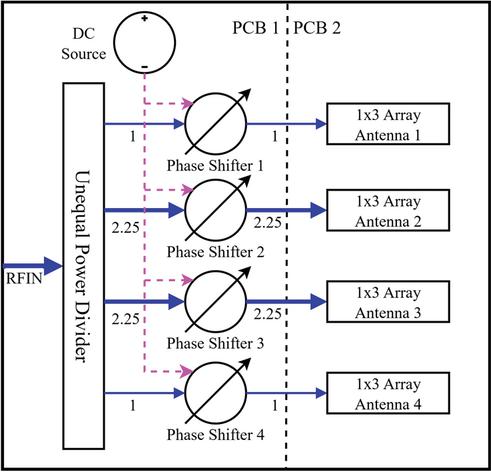
Figure 1 Structure of the phased array antenna.
Figure 1 shows the structure of the phased array antenna, which consists of two PCBs. PCB1 is responsible for RF power distribution and phase control. When the RF signal enters the unequal power divider, it is divided into four output ports with a power ratio of 1:2.25:2.25:1, respectively. Each output port is connected to a phase shifter for RF phase control, where each phase shifter requires a DC bias voltage to achieve the desired phase adjustment. PCB2 is responsible for radiating the RF power, consisting of four sets of array antennas that correspond to the four phase shifter outputs. The following sections present the design methodology at the operating frequency of 3 GHz, together with the simulation and measurement results of these components. The simulations were performed using Ansys HFSS and Keysight ADS, while the measurements were conducted with a Keysight P9371A VNA. All PCB simulations and fabrications were carried out on an FR4 substrate with a relative permittivity of 4.4, a loss tangent of 0.02, a thickness of 0.8 mm, and 1 oz copper cladding.
2.1 Design of the unequal power divider
In array antenna design, one important consideration is the suppression side lobe level [10, 11]. The most widely used approach is the optimum amplitude distribution, in which Dolph-Tschebyscheff distribution [12] is applied to calculate the input power of each array element. Since the proposed array antenna is a patch-type antenna with an inherent reflector, our experience shows that one of the standard Dolph-Tschebyscheff distribution equations must be modified accordingly, as shown in:
| (1) |
where denotes the voltage ratio, is expressed in dB, and represents the modified term.
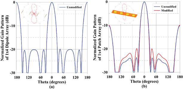
Figure 2 Normalized gain pattern: (a) dipole array, (b) patch array.
Figure 2 shows the normalized gain patterns of a dipole array antenna and a patch array antenna. In Fig. 2 (a), the unmodified pattern of the dipole array antenna is illustrated, where SSL is set to 20 dB with each port excited at a power ratio of 1:3:3:1. Figure 2 (b) compares the unmodified and modified patterns of the patch array antenna. The modified design achieves the desired SSL of 20 dB with a power ratio of 1:2.25:2.25:1, while the unmodified pattern shows a significantly degraded SSL, reduced by approximately 8 dB. Because the reflected power is superimposed on the original directional power, a modified term of must be included in (1) to modify the excitation power ratio, ensuring the designed SSL is accurate.
Based on the above analysis for achieving an SSL of 20 dB at patch array antenna, the output power ratio of the unequal power divider must be 1:2.25:2.25:1. This ratio is then applied to determine the impedance of each output port in the design of the unequal power divider. Furthermore, since each output port must maintain the same phase, a two-layer T-junction circuit structure is employed to design the unequal power divider, as shown in Fig. 3 (a).
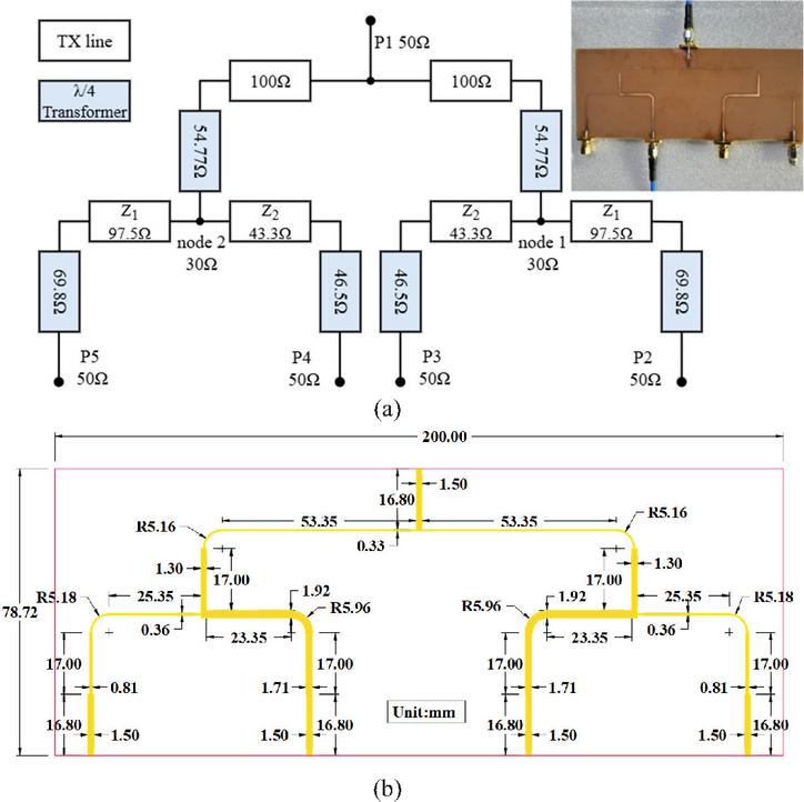
Figure 3 (a) Circuit structure and prototype of the unequal power divider. (b) Detailed dimensions of the unequal power divider in mm.
The unequal power divider adopts a symmetric structure, so only half of the circuit needs to be designed and then mirrored to form the complete structure. The key design consideration is determining the impedances and to achieve the desired output power ratio of at ports P3 and P2. Here, the calculation first employs the electric power formula in:
| (2) |
Assume that node 1 has a voltage and an impedance of , while the other end of and are connected to ground. Accordingly, the power ratio of P2 and P1 can be formulated as:
| (3) |
Moreover, by applying the parallel resistance formula, another equation can be obtained as:
| (4) |
Using (3) and (4), the impedances of and can be calculated. plays an important role in controlling ; if becomes too large, it may lead to manufacturing issues in the transmission line. All transmission line impedance values of the unequal power divider are designed and assigned as shown in Fig. 3 (a). Detailed dimensions are shown in Fig. 3 (b).
Figure 4 (a) presents the simulated and measured S-parameters of the unequal power divider. The measured exhibits a frequency offset of 50 MHz, shifting the resonance to 2.95 GHz; however, this deviation does not significantly affect the overall performance.
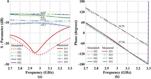
Figure 4 Simulated and measured results of the unequal power divider: (a) S-parameters and (b) phase response.
Furthermore, remains below 10 dB within the observed bandwidth of 600 MHz. Theoretically, the power ratio of 1:2.25:2.25:1 corresponds to 8.13 dB, 4.6 dB, 4.6 dB, and 8.13 dB, respectively. At 3 GHz, both the measured and simulated results are lower than the theoretical values. Specifically, and are approximately 6.6 dB and 6.02 dB, while and are approximately 10.3 dB and 9.25 dB. Although the measured results exhibit higher loss, the output power ratio still remains approximately 2.25:1. Figure 4 (b) shows the simulated and measured phase of the unequal power divider. The results remain in phase across the observed bandwidth; however, the measured data exhibits an additional phase delay of approximately at 3 GHz, which is attributed to the SMA connectors and does not impact the overall performance. From the above discussion, the unequal power divider is successfully designed to meet the requirements, achieving an output power ratio of 1:2.25:2.25:1 with all ports in phase.
2.2 The phase shifter
The phase shifter is a critical component in phased array antennas as it directly controls the main beam steering. The phase shifter employed in this work has been designed and analyzed in detail with the results in [13]. It provides a linear, continuous, and tunable phase response within . Furthermore, the tunable phase response includes both leading and lagging phases, which can be easily controlled by adjusting the DC bias voltage.
Figure 5 presents the equivalent circuit model of the phase shifter, whose structure enables the above description properties. In addition, the proposed phase shifter includes a design guideline that allows arbitrary design of its operating frequency and phase shifting bandwidth (PSBW). These phase shifters are designed for an operating frequency of 3 GHz with a PSBW of 400 MHz in this paper.
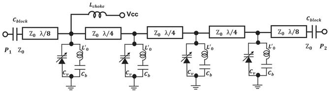
Figure 5 Equivalent circuit model of the phase shifter.
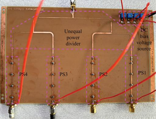
Figure 6 PCB1 prototype including the unequal power divider, four phase shifters, and four DC sources.
Figure 6 shows the prototype of PCB1, which includes the unequal power divider, four phase shifters, and four DC sources. The DC source (lumped components) consists of a 10 k variable resistor in series with a 2 k resistor to form a voltage divider circuit, which outputs a DC bias voltage to control the phase of the phase shifter. The measurement results of the prototype are presented in Fig. 7. Figure 7 (a) shows a resonance at 3 GHz with a minimum reflection coefficient of 20 dB, remaining below 6 dB within the observed bandwidth. It also exhibits two sets of transmission coefficients at approximately 14 dB and 20 dB, respectively. These losses are consistent with expectations, as the additional transmission loss introduced by the phase shifter is approximately 8 dB, compared to 6 dB and 10 dB for the case with only the power divider.
Figure 7 (b) shows the phase responses of the four output ports of the PCB1 prototype. At 3 GHz, the responses are clearly in phase, corresponding to . Furthermore, the responses exhibit an approximately linear phase variation within over the frequency range from 2.8 GHz to 3.16 GHz. This frequency range is important, as it also represents the tunable phase range of each phase shifter.
Figure 8 shows the measured phase response of each phase shifter with respect to the applied DC bias voltage at 3 GHz. All curves exhibit a similar trend, where adjusting the DC bias voltage from 3.5 V to 12 V results in a corresponding phase shift from to .
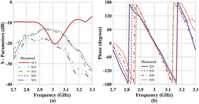
Figure 7 Measurement results of the PCB1 prototype: (a) S-parameters and (b) phase response.
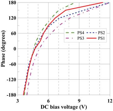
Figure 8 Measured phase response of each phase shifter corresponding to the control voltage.
The curve of PS4 reaches a phase shift at a bias voltage of 8.5 V, indicating that varactor diodes in this phase shifter exhibit slightly different characteristics as shown in Fig. 5. It should be noted that because the DC bias voltage is continuously adjustable, the phase shift also changes continuously. Consequently, the main beam steering of the phased array antenna is naturally continuous as well.
2.3 Design of the 4 3 array antenna
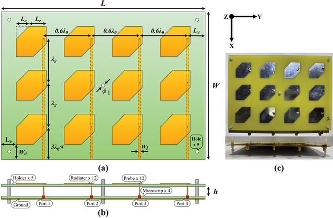
Figure 9 Structure of the array antenna: (a) top view, (b) front view, and (c) prototype.
Table 1 Design parameters of the array antenna
| Unit | ||||||
| 255 | 16 | 21.5 | 18.75 | 22.5 | 6 | |
| mm | ||||||
| 185 | 18.75 | 3 | 100 | 55 | 4 |
Figure 9 illustrates the structure and prototype of the array antenna, comprising two FR4 PCBs. The upper PCB consists of 12 hexagon radiators arranged in a configuration, with an element spacing of along the Y-axis and along the X-axis. The lower PCB consists of four feeding lines and a ground plane. The two PCBs are assembled using five holders with a separation distance of . The distance is designed to enhance the radiation efficiency of the patch antenna [14]. The 12 radiators are connected to their corresponding feeding lines through 12 copper wires. Each copper wire has a diameter of 1 mm. Table 1 lists all design parameters of the array antenna.
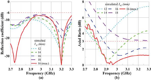
Figure 10 Simulated and measured results of the array antenna: (a) reflection coefficient and (b) axial ratio.
Figure 10 (a) shows the simulated and measured reflection coefficients of a single port of the array antenna, along with the results obtained for different corner-cut lengths of the rectangular patch. The corner-cut is introduced to improve the circular polarization radiation characteristics of the array antenna. The axial ratio (AR) is a key indicator for evaluating whether an antenna exhibits circular polarization, with a threshold of 3 dB commonly used to assess circular polarization performance. However, a of 16 mm was selected, as it provides the best AR bandwidth, as shown in Fig. 10 (b), with only a slight degradation in the reflection coefficient. Therefore, in this case, the reflection coefficient and AR exhibit a trade-off. To achieve a better AR, we slightly sacrifice the reflection coefficient, which degrades to 8 dB at 3 GHz. Figure 10 illustrates the measured results (red lines) are better overall than the simulated results. In general, a reflection coefficient below 6 dB is considered acceptable in industry standards. If this criterion is adopted, the bandwidth of the antenna array exceeds 600 MHz, as shown in Fig. 10 (a).
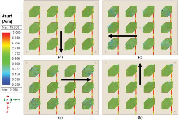
Figure 11 Current distribution of the RHCP at 3 GHz: (a) , (b) , (c) , (d) .
Figure 11 shows the current distribution of the RHCP at 3 GHz, with four identical current directions at , and , respectively. In addition, the feeding spacing of ensures that the currents of all 12 radiators and feeding lines remain in phase. A uniform current distribution is observed on each radiator along the four directions.
The isolation is an important evaluation index for reducing interference in array antennas. In general, the isolation should be lower than 20 dB, which indicates that the mutual coupling power between elements is less than 1/100. As shown in Fig. 12, both the simulated and measured isolation values are all below 23 dB, meaning that the coupling power between each port of the array antenna is less than , thereby achieving good isolation performance.
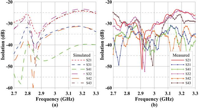
Figure 12 Isolation of the array antenna: (a) simulated and (b) measured.
Figure 13 shows a 3D gain pattern and measurement setup of the array antenna with an unequal power divider. The 3D gain pattern demonstrates a maximum gain of 15.11 dB, with suppressed side-lobes in the Y-Z plane, when the four ports are excited with a power ratio of 1:2.25:2.25:1.
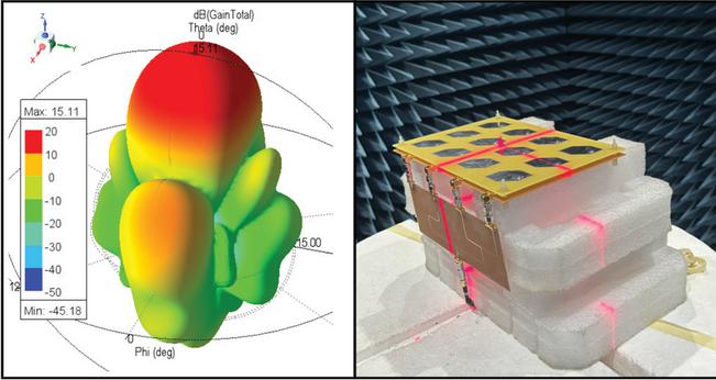
Figure 13 3D gain pattern and measurement setup of the array antenna with an unequal power divider.
Figure 14 compares the simulated and measured 2D gain patterns in the X-Z and Y-Z planes. Both results exhibit similar trends; however, the angular resolution differs, being in simulation and in measurement. The resolution in the measurements also leads to a more symmetric radiation pattern. The measured maximum gain is 13.68 dB, which is lower than the simulated value due to approximately 1.43 dB of insertion loss introduced by the five SMA connectors. Moreover, the measured side-lobe levels are below 20 dB on both sides, confirming the effective side-lobe suppression achieved by the unequal power divider, as shown in Fig. 14 (b). In addition, the measured half-power beamwidth is approximately , which is consistent with the simulated result.
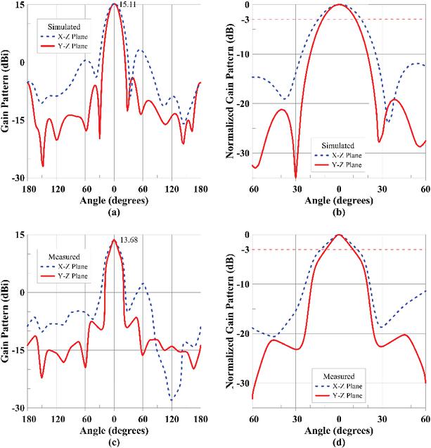
Figure 14 Comparison of 2D gain patterns in the X-Z and Y-Z planes: (a,b) simulated and (c,d) measured.
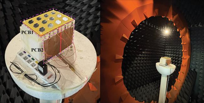
Figure 15 Measurement setup of the phased array antenna.
3 PHASED ARRAY ANTENNA
Figure 15 shows the measurement setup of the phased array antenna, where PCB1 and PCB2 are connected using four L-shaped SMA connectors. The measurement setup employs the ETS-Lindgren’s AMS 8923-14-G Antenna Measurement System.
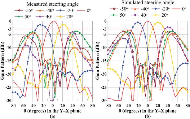
Figure 16 (a) Measured and (b) simulated steering angle of the phased array antenna.
Table 2 Steering angle of the phased array antenna corresponds to the phase difference and control voltage of each phase shifter
| Steering | ||||||||||||||
| angle | V | V | V | V | V | V | V | |||||||
| PS1 | 3.5 | 3.7 | 4 | 4.7 | 7 | 7.5 | 4.7 | |||||||
| PS2 | 4.6 | 4.6 | 4.6 | 4.6 | 5.6 | 4.6 | 3.4 | |||||||
| PS3 | 12 | 10 | 6.5 | 5.1 | 5.1 | 3.7 | 5.1 | |||||||
| PS4 | () | 4.5 | () | 4.2 | 7 | 4.5 | 4 | () | 5.1 | 3.5 | ||||
Table 3 Comparison of the proposed phased array antenna with other designs
| Ref. | Technology | Control Voltage | Steering Type | Steering Range | Complexity/Cost |
| [6] | Passive Butler matrix | N/A | Discrete | 4 fixed angles | Low |
| [7] | Ferroelectric | Continuous | Medium | ||
| [9] | RF MEMS | Continuous | High | ||
| This Work | Varactor based phase shifters | Continuous | Low |
Figure 16 shows the measured and simulated gain patterns of the phased array antenna at different steering angles. Since the measured gain was compensated for the 10 dB loss introduced by the phase shifters, the patterns are nearly identical in shape. Even after compensation, the measured gain is still about 3 dB lower than the simulated gain, which can be attributed to losses from the connectors and substrates. Figure 16 (b) shows the simulated maximum steering angle from to in the Y-Z plane. This indicates that when the main beam is steered to its maximum angle, a secondary main beam appears at the opposite angle. A similar situation can also be observed in the measurements, where a secondary main beam appears, though smaller than the primary beam. The measured steering angle ranges from to in the Y-Z plane, which is wider than the simulated result. This discrepancy may be attributed to measurement errors according to:
| (5) |
where is the wave number, d is the element spacing, is the azimuth angle, is the phase difference. In other words, the azimuth angle corresponding to the required phase difference can be easily calculated. Furthermore, each phase difference can be mapped to a control voltage for each phase shifter, as illustrated in Fig. 8. Table 2 summarizes the steering angles of the phased array antenna along with the corresponding phase differences and control voltages. It is worth noting from Table 2 that the phase differences are relative, incorporating both leading and lagging phases. In contrast, most other phase shifters employ only lagging phases and achieve phase shifting in discrete steps. Furthermore, since the control voltage is continuously adjustable, the corresponding phase variation is also continuous. These two features represent the major contributions of the proposed electronically continuous tunable phased array antenna.
4 COMPARISON WITH OTHER DESIGNS
Table 3 compares the proposed phased array antenna with other reported phased array systems. The Butler matrix-fed design in [6] is low cost and suitable for mmWave 5G applications, but its discrete phase states restrict beam steering to only four directions.
Ferroelectric-based phase shifters [7] allow continuous tuning, but the high control voltage (150 V) raises safety and integration concerns. MEMS-based phase shifters [9] provide precise phase control; however, their complex fabrication increases cost, and the achieved steering angle is typically narrow .
In contrast, the proposed phased array antenna achieves wide-angle steering (), robust circular polarization, and continuous tunability with a safe and low control voltage (). Additionally, its structure is relatively simple, leading to lower cost and higher manufacturability. These advantages make it an attractive candidate for practical microwave and wireless communication applications.
5 CONCLUSION
In this work, an electronically continuous tunable phased array antenna operating at 3 GHz has been proposed and demonstrated. The design integrates an unequal power divider, four electronically continuous tunable phase shifters, and a RHCP patch array antenna. The unequal power divider achieves the optimized power ratio of 1:2.25:2.25:1, effectively suppressing the SSL by 20 dB.
The proposed phase shifter provides linear, continuous, and wide-range phase control within , which can be easily adjusted via a DC bias voltage. Unlike conventional phase shifters that typically offer only lagging phase (phase delay), the proposed design enables both leading and lagging phases. This capability significantly enhances beam-steering flexibility. Consequently, a wide steering range from to is achieved without the need for complex phase-wrapping algorithms commonly required in conventional designs.
The array antenna, consisting of 12 hexagon shaped patches, achieves RHCP across the operating bandwidth, a high gain of 13.68 dB, and excellent isolation performance with all port coupling below 23 dB. Beam steering from to in the Y-Z plane has been experimentally verified, with measured results showing good agreement with simulations. Overall, the proposed phased array antenna demonstrates high gain, robust RHCP, low SSL, low isolation, wide-angle beam steering, and continuous phase control, which are key features required for future microwave and wireless communication applications.
ACKNOWLEDGMENT
This work was supported by the National Science and Technology Council, Taiwan, under Contract NSTC 113-2221-E-011-110-MY2. The authors would like to thank HONGBO Wireless Communication Technology Co. Ltd. for providing access to the radio wave anechoic chamber for the phased array antenna measurements.
REFERENCES
[1] T. Chaloun, L. Boccia, E. Arnieri, M. Fischer, V. Valenta, and N. J. G. Fonseca, “Electronically steerable antennas for future heterogeneous communication networks: Review and perspectives,” IEEE Journal of Microwaves, vol. 2, no. 4, pp. 545–581, 2022.
[2] H. Lee, S. Kim, and J. Choi, “A 28 GHz 5G phased array antenna with air-hole slots for beam width enhancement,” Applied Sciences, vol. 9, no. 20, 2019.
[3] O. Barrou, A. El Amri, and A. Reha, “Microstrip patch antenna array and its applications: A survey,” IOSR Journal of Electrical and Electronics Engineering, vol. 15, no. 1, pp. 26–38, 2020.
[4] M. Li, S.-L. Chen, Y. Liu, and Y. J. Guo, “Wide-angle beam scanning phased array antennas: A review,” IEEE Open Journal of Antennas and Propagation, vol. 4, pp. 695–712, 2023.
[5] M. Kebe, M. C. E. Yagoub, and R. E. Amaya, “A survey of phase shifters for microwave phased array systems,” International Journal of Circuit Theory and Applications, vol. 53, no. 6, pp. 3719–3739, 2024.
[6] C. K. Lin, D. B. Lin, and M. L. Chang, “A low-cost 44 Butler matrix-fed patch antenna array for millimeter wave applications,” Microwave and Optical Technology Letters, vol. 67, no. 1, 2025.
[7] M. Sazegar, Y. Zheng, H. Maune, C. Damm, X. Zhou, and J. Binder, “Low-cost phased-array antenna using compact tunable phase shifters based on ferroelectric ceramics,” IEEE Trans. Microw. Theory Techn., vol. 59, no. 5, pp. 1265–1273, 2011.
[8] E. Liu, G. Li, Y. Zhao, and Y. Zhao, “Design of an X-band 4-channel circulator phase shifter based on silicon MEMS technology,” in 2025 5th International Conference on Electronics, Circuits and Information Engineering (ECIE), pp. 610–615, 2025.
[9] P. Goel and K. Vinoy, “A low-cost phased array antenna integrated with phase shifters cofabricated on the laminate,” Progress in Electromagnetics Research B, vol. 30, pp. 255–277, 2011.
[10] M. Arun and M. R. Ebenezar Jebarani, “Design of phased array antenna with low side lobes,” Materials Today: Proceedings, vol. 80, pp. 2150–2154, 2023.
[11] F. Y. Zulkifli, T. Hidayat, and E. T. Rahardjo, “Sidelobe level suppression using unequal four-way power divider for proximity coupled microstrip antenna,” in 2013 Asia-Pacific Microwave Conference Proceedings (APMC), pp. 1166–1168, 2013.
[12] C. A. Balanis, Antenna Theory: Analysis and Design. Hoboken, NJ: John Wiley & Sons, 2016.
[13] C.-K. Lin and D.-B. Lin, “Design and analysis of an electronically continuous tunable phase shifter for phased array antennas,” IEICE Transactions on Fundamentals of Electronics, Communications and Computer Sciences, pp. 873–883, 2025.
[14] D.-B. Lin, C.-K. Yu, C.-K. Lin, and Y.-H. Lee, “Dual band rectenna with one rectifier,” in 2017 International Symposium on Electronics and Smart Devices (ISESD), pp. 268–272, 2017.
BIOGRAPHIES

Chang-Keng Lin was born in New Taipei City, Taiwan. He received his M.S. degree in Electronic Engineering from the National Taipei University of Technology, Taipei, in 2016. He received his Ph.D. degree in the Department of Electronic and Computer Engineering at the National Taiwan University of Science and Technology, Taipei, in 2026. His research interests include phase shifters, phased-array antennas, microwave components, antennas, wireless power transfer, RF circuits, and electronic circuit integration.

Ding-Bing Lin (S’89–M’93–SM’14) received the M.S. and Ph.D. degrees in electrical engineering from National Taiwan University, Taipei, Taiwan, in 1989 and 1993, respectively. From August 1993 to July 2016, Lin was on the faculty of the Electronic Engineering Department, National Taipei University of Technology, Taipei, where he was an Associate Professor, a Professor, and a Distinguished Professor in 1993, 2005, and 2014 respectively. Since August 2016, he had been with National Taiwan University of Science and Technology, Taipei, where he is currently a Professor of the Electronic and Computer Engineering Department. His research interests include wireless communication, antennas, high-speed digital transmission, and microwave engineering. From 2015 to 2018, he served as the Taipei Chapter Chair, IEEE EMC society. Since 2022, he serves as Taipei Chapter Chair, IEEE AP Society. Since 2019, he serves as Associate Editor of IEEE Transactions of Electromagnetic Compatibility and since 2014 as Editorial Board member of International Journal of Antennas and Propagation. He has published more than 250 papers in international journals and conferences. Lin was the recipient of the Annual Research Outstanding Award of the College of Electrical Engineering and Computer Science in 2004, 2006, and 2008. After he had received these three awards, the College of Electrical Engineering and Computer Science awarded him the College Research Outstanding Award to highlight his research achievements. He was also the recipient of the Taipei Tech Annual Outstanding Research Award in 2008. Lin is the recipient of the Annual Research Outstanding Award of the National Taiwan University of Science and Technology in 2024.

Chang-Ching Lin was born in Yun Lin County, Taiwan. He received his M.S degree in Electrical and Communication Engineering from Yuan Ze University in 2010. From 2004 to 2008, he worked at Amphenol Antenna Taiwan Center. From 2008 to 2017, he worked at Foxconn FIT Antenna Team. Since 2017, he has been working at Hong-Bo Wireless Technology, mainly focusing on the design of commercial embedded antennas.
ACES JOURNAL, Vol. 41, No. 4, 334–342
DOI: 10.13052/2026.ACES.J.410405
© 2025 River Publishers