A Miniaturized Wilkinson Power Divider with Integrated Phase Shifter
Thanapat Chiawchanwattana1, Ravee Phomloungsri2, Somkuan Srisawat2, Niwat Angkawisittpan3*, and Sivarit Sultornsanee4
1Department of Electrical and Computer Engineering Faculty of Engineering, Mahasarakham University, Maha Sarakham 44150, Thailand
65010393001@msu.ac.th
2Department of Computer and Communication Engineering Faculty of Technology and Engineering Udon Thani Rajabhat University, Udon Thani, 41000, Thailand
phravee@gmail.com, somkaun.srisawat@gmail.com
3Research Unit for Electrical and Computer Engineering Faculty of Engineering, Mahasarakham University, Maha Sarakham 44150, Thailand
∗niwat.a@msu.ac.th
4College of Engineering Northeastern University, Boston, Massachusetts, 02115, USA
s.sultornsanee@northeastern.edu
Submitted On: January 19, 2026
Accepted On: May 12, 2026
ABSTRACT
This paper reports the design of a compact Wilkinson power divider for use in modern wireless communication systems where circuit size is a critical constraint. The proposed design replaces the conventional quarter-wavelength transmission line with a compact phase-shifting section based on parallel-coupled microstrip lines, providing an impedance transformation factor of for proper matching to a 50 system. The power divider is designed to operate at a center frequency of 3.0 GHz on an AD260 substrate, with the phase-shifting function directly integrated into the power-dividing network to reduce the overall circuit footprint. The fabricated prototype occupies an area of , corresponding to a size reduction of approximately 22% compared with a conventional Wilkinson power divider. Simulation results obtained using Advanced Design System (ADS) demonstrate strong agreement, with a return loss () better than 15 dB and insertion losses ( and ) close to the ideal value of dB at the operating frequency. The fabricated prototype was characterized over the 2–6 GHz frequency range, demonstrating strong agreement with the simulated results. These results indicate that the proposed structure achieves effective power division with good impedance matching while maintaining a compact size, making it suitable for integration into compact RF and microwave front-end circuits.
Keywords: Circuit miniaturization, parallel-coupled microstrip lines, phase compensation, Wilkinson power divider..
1 INTRODUCTION
Recent advances in wireless communication technologies have driven the demand for compact, lightweight, and high-performance RF and microwave circuits. Modern applications such as mobile terminals, wearable devices, Internet of Things (IoT) nodes, and vehicle-to-everything (V2X) communication systems require circuit components that not only provide reliable electrical performance but also occupy minimal physical area [1]. As a result, circuit miniaturization has become a key research topic in the development of next-generation wireless front-end systems.
Table 1 Summary of reported miniaturization techniques for Wilkinson power dividers
| Ref. | Technique | Main Advantage | Limitation |
| [2] | 3-D MMIC integration | Significant size reduction achieved through three-dimensional integration | Complex fabrication process and higher manufacturing cost |
| [3] | Capacitive loading | Compact circuit realization with reduced physical length | Narrow operating bandwidth |
| [4] | Active inductors | Effective size reduction using active circuit elements | Additional biasing circuitry and power consumption |
| [5] | T-shaped transmission lines | Simple planar layout with moderate size reduction | Limited miniaturization capability |
| [6] | Fractal structure | Harmonic suppression and size reduction | Increased design and optimization complexity |
| [7] | Resonator-based design | Harmonic control and performance enhancement | Increased layout area compared with simple structures |
| This work | Coupled-line phase shifter | Compact and planar structure with integrated phase-shifting functionality | Required optimization for impedance and phase balance |
The Wilkinson power divider is a fundamental building block widely used in RF and microwave systems for power distribution, signal combining, and antenna feeding networks. In response to stringent size constraints, numerous miniaturization techniques for Wilkinson power dividers have been reported in the literature. These include three-dimensional integration technologies [2], lumped-element realizations [8, 9], inductive and capacitive loading methods [3, 4, 10, 11], T-shaped transmission-line configurations [5, 12], fractal-based structures [6], and resonator-assisted designs [1, 7, 13]. While these approaches can effectively reduce circuit size, they often involve trade-offs in bandwidth, fabrication complexity, or design flexibility. A summary of representative miniaturization techniques for Wilkinson power dividers reported in the literature is provided in Table 1. It should be noted that the proposed design employs a lumped capacitor for capacitive compensation, whereas some reported works are based solely on transmission-line structures. The inclusion of a lumped element in this work is intended to provide a simple and practical means for phase adjustment without significantly increasing circuit complexity. Therefore, the comparison focuses on overall design strategy and performance trade-offs rather than strict structural equivalence.
As shown in Table 1, most existing miniaturization approaches achieve size reduction at the expense of increased design complexity, limited bandwidth, or fabrication challenges. This observation motivates the exploration of alternative compact structures that can provide circuit miniaturization while maintaining acceptable electrical performance.
Parallel-coupled microstrip lines have been extensively employed in the realization of compact microwave components, including bandpass filters, impedance transformers, and phase shifters [14, 15, 16, 17, 18]. In particular, coupled-line-based phase shifter configurations, such as Schiffman-type and differential phase shifters, have attracted significant attention due to their planar structure, broadband characteristics, and compatibility with standard fabrication processes. These designs exploit the electromagnetic coupling between adjacent transmission lines to introduce a desired phase delay within a reduced physical length. Despite their advantages, microstrip coupled-line structures inherently suffer from unequal phase velocities between the even and odd propagation modes as a result of dielectric inhomogeneity. This phase imbalance can lead to deviations from the intended phase response, increased insertion loss, and degraded isolation when such structures are integrated into power-dividing or signal-combining networks. To overcome these limitations, a wide range of compensation techniques has been proposed, including capacitive and inductive loading methods, dielectric overlays, and hybrid compensation schemes [19, 20, 21, 22, 23, 24, 25, 26, 27, 28, 29, 30, 31, 32, 33]. These approaches provide important design insights for improving the performance of coupled-line-based circuits.
Although a variety of miniaturization techniques have been reported, such as slow-wave structures, defected ground structures (DGS), meandered transmission lines, and lumped-element loading, each approach has certain limitations. For instance, slow-wave and DGS-based techniques often require complex geometrical modifications and may increase fabrication complexity, while lumped-element approaches introduce additional parasitic effects and may limit bandwidth performance. In contrast, the proposed design employs a capacitive-compensated parallel-coupled microstrip structure, which provides a simple planar implementation without requiring multilayer configurations or intricate layouts. This approach enables effective size reduction while maintaining good impedance matching,power division, and isolation characteristics, making it more suitable for practical RF and microwave circuit integration.
In this work, a compact Wilkinson power divider operating at 3.0 GHz is proposed by replacing the conventional quarter-wavelength transmission line with a 90∘ phase-shifting section implemented using parallel-coupled microstrip lines. Based on even- and odd-mode analysis, the coupled-line section is designed to provide a characteristic impedance of , enabling the required impedance transformation while occupying a shorter physical length than a traditional line. By integrating the phase-shifting function directly into the power-dividing network, the proposed design achieves circuit miniaturization without significantly compromising electrical performance.
2 DESIGN AND ANALYSIS
2.1 Design principle of the capacitive compensated coupled-line structure
In RF and microwave circuit design, the physical length of quarter-wavelength () transmission lines often limits circuit miniaturization. To address this issue, a compact phase-shifting structure based on parallel-coupled microstrip lines with capacitive compensation is proposed to emulate the electrical behavior of a conventional quarter-wavelength transmission line.
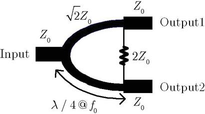
Figure 1 Conventional Wilkinson power divider with quarter-wavelength transmission lines.
Figure 1 illustrates a conventional Wilkinson power divider, where two transmission lines with characteristic impedance provide impedance matching and equal power division, while an isolation resistor of ensures high isolation between output ports. Although excellent electrical performance is achieved, the quarter-wavelength sections result in a relatively large physical footprint.
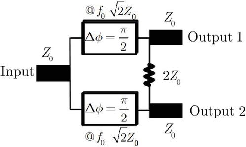
Figure 2 Proposed Wilkinson power divider using integrated phase-shifting sections.
To achieve size reduction, the proposed design replaces the conventional transmission lines with compact phase-shifting sections, as shown in Fig. 2. Each phase-shifting section is designed to provide an electrical phase delay of and an equivalent characteristic impedance of at the operating frequency . This approach preserves the required impedance transformation while significantly reducing the circuit size.
The proposed phase-shifting section is realized using a parallel-coupled microstrip line with even- and odd-mode impedances and , respectively, and an electrical length . Due to dielectric inhomogeneity, the even- and odd-mode phase velocities are generally unequal, which degrades circuit performance as in Fig. 3 shows the equivalent two-port network of the capacitive-compensated coupled-line structure. To compensate for this effect, a lumped capacitor with impedance is connected between the open-circuited ports of the coupled-line section.
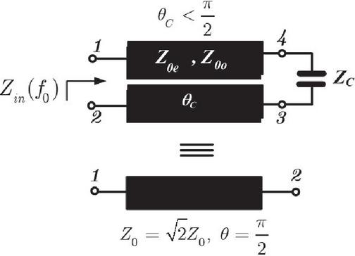
Figure 3 Equivalent two-port network of the capacitive-compensated coupled-line structure.
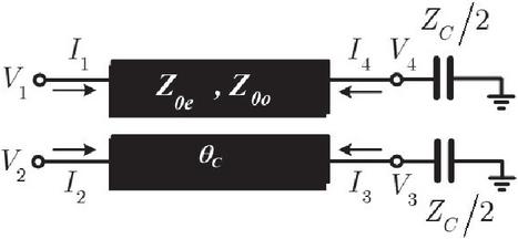
Figure 4 Voltage–current definition of the capacitive-compensated coupled-line structure for circuit analysis.
For circuit analysis, the coupled-line structure is initially represented as a four-port network. By symmetrically terminating Ports 3 and 4 with shunt capacitive impedances of , the network can be reduced to an equivalent symmetric two-port representation, as illustrated in Fig. 4. This shunt capacitive loading primarily introduces an additional phase delay to the odd mode, thereby compensating for the phase velocity mismatch. Physically, the compensation capacitor introduces an additional reactive loading to the coupled-line section, which modifies the phase response of the structure. Since the odd mode is more sensitive to the electric-field distribution between the coupled strips, the shunt capacitive loading predominantly affects the odd-mode propagation, introducing an additional phase delay. In contrast, the even mode is comparatively less affected because its field distribution is less concentrated across the coupled region. As a result, the capacitor helps reduce the phase velocity imbalance between the even and odd modes, enabling the shortened coupled-line section to more closely emulate the phase behavior of a conventional quarter-wavelength transmission line.
1. Equivalent two-port impedance representation Under the assumptions of reciprocity and symmetry, the equivalent two-port impedance parameters of the capacitive-compensated coupled-line structure [29, 33] can be expressed as:
| (1) |
Because the proposed structure is geometrically symmetric with respect to the input and output planes and consists of passive reciprocal elements, the impedance matrix exhibits both symmetry and reciprocity [33]. Accordingly, the diagonal elements satisfy and , whereas the off-diagonal terms follow , , and . Ports 3 and 4 are terminated by shunt capacitive impedances , yielding
| (2) |
By applying the symmetry conditions and imposing the current relationship at Ports 3 and 4 (i.e., ), the four-port impedance equations can be reduced to
| (3) | ||
After applying the capacitive boundary conditions and reducing the four-port description to an equivalent two-port network, the resulting voltage–current relations can be expressed as
| (4) | |
| (5) |
Equations (4)–(5) indicate that the capacitive-compensated coupled-line section can be represented by an equivalent symmetric two-port -parameter matrix. For compactness, define
| (6) |
The parameter represents the effective impedance contribution introduced by the combined effect of the coupling difference and the shunt capacitive loading. Thus, the equivalent two-port representation is written as
| (7) |
where captures the combined effect of the coupling imbalance and the shunt capacitive loading, enabling the shortened coupled-line section to emulate a quarter-wavelength impedance inverter at the design frequency.
| (8) | ||
Therefore, the equivalent two-port network can be written in matrix form as
| (9) |
Accordingly, the voltage–current relationship of the proposed structure can be written in the standard two-port impedance matrix form as
| (10) |
The parameter represents the combined effect of coupling imbalance and shunt capacitive loading, enabling the shortened coupled-line section to emulate a quarter-wavelength impedance inverter.
2. Input matching condition From the equivalent two-port impedance matrix in (10), the input reflection coefficient can be expressed in terms of the -parameters as [29, 33]
| (11) |
The input reflection coefficient of the equivalent two-port network is given by
| (12) |
Perfect input matching at the design frequency is achieved when , which yields a closed-form expression for the required capacitive impedance .
3. Physical design parameters The required shunt capacitance can be obtained from
| (13) |
where . The electrical length of the shortened coupled-line section is determined by
| (14) |
with
| (15) |
representing the phase velocity ratio between the odd and even modes.
4. Transmission performance Finally, the transmission coefficient of the synthesized two-port network is expressed as
| (16) |
or equivalently,
| (17) |
Equation (17) confirms that the transmission performance of the proposed capacitive-compensated coupled-line structure is directly governed by the synthesized impedance parameter , enabling equal power division while maintaining a compact circuit footprint.
2.2 Impedance transformation and electrical length adjustment of the capacitive-compensated parallel-coupled transmission line
To quantitatively describe the compensation behavior, the synthesized values of the shunt capacitance and the shortened electrical length were extracted for coupling levels ranging from to dB. The coupling range from to dB was selected because it represents a practical design interval for parallel-coupled microstrip lines at 3.0 GHz, where the coupling strength is sufficiently high to support compact phase-shifter implementation while still maintaining realizable physical dimensions and acceptable fabrication tolerance.
In addition to circuit miniaturization, the proposed capacitive-compensated parallel-coupled transmission line must simultaneously satisfy two essential design requirements: impedance transformation and precise electrical length control. In a conventional Wilkinson power divider, each quarter-wavelength () transmission line provides both a phase shift and an impedance transformation from to . When the physical length of the transmission line is reduced, these two functions must be preserved through appropriate circuit synthesis. In the proposed structure, the impedance transformation is achieved through the even- and odd-mode characteristic impedances of the parallel-coupled microstrip lines. By properly selecting and , the coupled-line section can be designed to exhibit an equivalent characteristic impedance of at the operating frequency. This behavior emulates the impedance-inverting property of a conventional quarter-wavelength transmission line while occupying a shorter physical length. However, due to dielectric inhomogeneity in microstrip structures, the even- and odd-mode phase velocities are generally unequal, causing a deviation from the desired electrical phase shift. To compensate for this effect, a shunt capacitor is introduced between the open-circuited ends of the coupled-line section. The capacitive loading effectively introduces an additional phase delay to the odd-mode propagation, while the even mode remains comparatively unaffected. As a result, the overall phase imbalance between the two modes is reduced. By appropriately selecting the value of the shunt capacitance , the shortened coupled-line section can be adjusted to provide an exact electrical phase shift at the design frequency , despite its reduced physical length. Consequently, the capacitive-compensated coupled-line structure simultaneously achieves impedance transformation and electrical length control, enabling it to serve as an electrically equivalent substitute for a conventional quarter-wavelength transmission line in compact Wilkinson power divider applications. To facilitate practical implementation, the design equations derived in the previous subsection are employed to determine suitable initial values for the physical and electrical parameters of the proposed structure. Specifically, the even- and odd-mode impedances, the shortened electrical length, and the shunt capacitance are jointly considered to ensure that both impedance matching and phase compensation conditions are satisfied at the operating frequency . In the synthesis procedure, the coupled-line geometry is first selected to achieve the required coupling coefficient, which directly governs the values of and . The physical dimensions of the coupled lines, including the conductor width , spacing , and coupling length , are then adjusted accordingly based on the chosen substrate parameters. In this work, the proposed structures are implemented on FR4 and AD260 substrates in order to investigate the influence of dielectric properties on the impedance transformation and phase response. After defining the coupled-line geometry, the shunt capacitive loading is introduced to compensate for the phase velocity mismatch between the even and odd modes. The value of is initially estimated using the derived closed-form expressions and subsequently refined through parametric optimization. The optimization process focuses on minimizing the input reflection coefficient while maintaining a transmission coefficient close to dB and achieving a phase shift of approximately at the design frequency. The electrical performance of the synthesized two-port network is evaluated in terms of its scattering parameters, namely , , and the phase of . These parameters provide direct insight into the impedance matching, insertion loss, and phase characteristics of the proposed structure. By systematically adjusting the coupled-line dimensions and the shunt capacitance , an optimal trade-off between size reduction and electrical performance can be achieved. To further elucidate the impedance transformation and phase compensation mechanism, Figs. 5–7 present the parametric synthesis results obtained for the FR4 substrate (). Figure 5 illustrates the variation of the required shunt capacitance and the shortened electrical length as functions of the coupling factor. As the magnitude of the coupling factor decreases (from to dB), the required compensation capacitance is reduced, while the effective electrical length shifts closer to the ideal condition. In general, stronger coupling requires a larger compensation capacitance and a corresponding adjustment of the electrical length to maintain the desired impedance transformation and phase response.
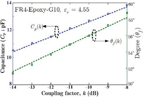
Figure 5 Relationship between shunt capacitance , shortened electrical length , and coupling factor for the FR4 substrate ().
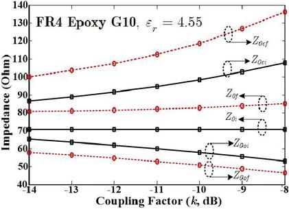
Figure 6 Initial and optimized even- and odd-mode impedances versus coupling factor for the FR4 substrate.
Table 2 Design parameters of the capacitive-compensated parallel-coupled transmission line implemented on FR4 substrate at 3.0 GHz for various coupling levels
| Coupling | Initial Impedance | Initial Dimensions | Optimized Impedance | Optimized Dimensions | and |
| (dB) | [mm] | [mm] | |||
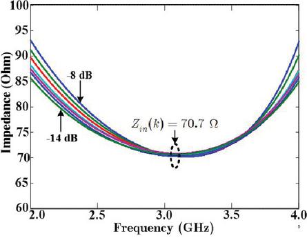
Figure 7 Input impedance versus frequency for different coupling factors on the FR4 substrate.
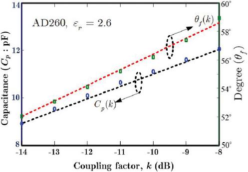
Figure 8 Variation of compensation capacitance and shortened electrical length versus coupling factor for the AD260 substrate ().
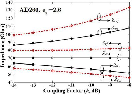
Figure 9 Initial and optimized even- and odd-mode impedances versus coupling factor for the AD260 substrate.
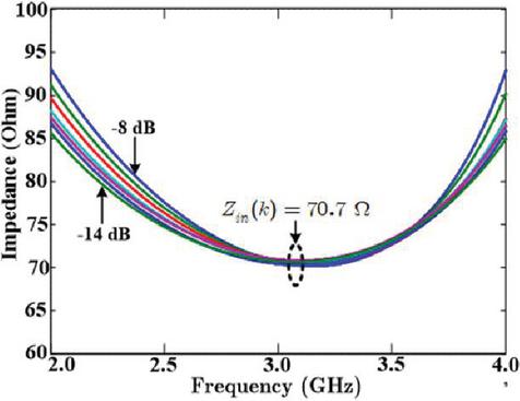
Figure 10 Input impedance versus frequency for different coupling levels on the AD260 substrate.
Table 3 Design parameters of the capacitive-compensated parallel-coupled transmission line implemented on AD260 substrate at 3.0 GHz for various coupling levels
| Coupling | Initial Impedance | Initial Dimensions | Optimized Impedance | Optimized Dimensions | Compensation |
| (dB) | [mm] | [mm] | |||
This behavior confirms that stronger electromagnetic coupling requires greater capacitive loading to mitigate the even–odd mode phase imbalance. Figure 6 presents the evolution of the even- and odd-mode impedances before and after optimization. It can be observed that the optimized values gradually approach the required impedance transformation condition of , ensuring that the synthesized section functions as an equivalent quarter-wavelength impedance inverter. Finally, Fig. 7 shows the input impedance response of the synthesized structure over frequency. All coupling scenarios exhibit an impedance minimum near at 3.0 GHz, validating that the proposed structure successfully preserves the impedance-inverting property at the design frequency. The corresponding synthesized design parameters for the FR4 substrate are summarized in Table 2. The table presents the initial and optimized even- and odd-mode impedances, physical dimensions, compensation capacitance, and shortened electrical length for coupling levels ranging from to dB. It can be observed that stronger coupling requires a larger compensation capacitance and a longer electrical length adjustment to satisfy the impedance transformation and phase compensation requirements. Similarly, Figs. 8–10 present the corresponding parametric results for the AD260 substrate (). Compared with FR4, the lower dielectric constant of AD260 modifies the even–odd mode field distribution, leading to slightly different compensation capacitance values and electrical lengths. Nevertheless, the same monotonic trend between coupling strength and required capacitive loading is clearly preserved. As shown in Fig. 9, the optimized even- and odd-mode impedances converge toward the target impedance transformation condition of , confirming that the proposed synthesis method is applicable to substrates with different dielectric constants. Finally, Fig. 10 confirms that the input impedance remains approximately at 3.0 GHz for all investigated coupling levels. This validates that the impedance-inverting property and phase compensation mechanism of the proposed capacitive-compensated coupled-line structure is robust with respect to substrate variation. The corresponding design parameters obtained for the AD260 substrate are listed in Table 3. Similar trends can be observed, where the required compensation capacitance and electrical length vary systematically with the coupling level. Compared with the FR4 substrate, the lower dielectric constant of AD260 results in slightly different optimized impedance values and compensation requirements while maintaining the desired impedance transformation characteristics at 3 GHz.
2.3 Impedance transformation and electrical length adjustment
To quantitatively describe the compensation behavior, the synthesized values of the shunt capacitance and the shortened electrical length were extracted for coupling levels ranging from to dB. Using the parametric data obtained from Fig. 5, a linear curve-fitting procedure was performed to establish approximate analytical relationships between the coupling factor (in dB), the required compensation capacitance, and the corresponding shortened electrical length. The fitted expressions are obtained as
| (18) | ||
| (19) |
where denotes the coupling factor in decibels (dB). Equations (18) and (19) indicate that both the compensation capacitance and the shortened electrical length exhibit an approximately linear dependence on the coupling level within the investigated design range. Specifically, as the magnitude of the coupling factor decreases (i.e., weaker coupling), the required shunt capacitance is reduced, while the electrical length shifts closer to the ideal condition. This behavior confirms that stronger coupling requires greater capacitive loading to compensate for the even–odd mode phase velocity imbalance. It should be noted that the above expressions are valid within the coupling range of dB and are intended to serve as practical design guidelines for rapid initial parameter estimation prior to full-wave optimization. In addition to the compensation capacitance and electrical length, Fig. 9 also reveals an approximately linear relationship between the coupling factor and the even- and odd-mode characteristic impedances for the AD260 substrate. By applying linear curve fitting within the range dB, the following empirical expressions are obtained:
| (20) | ||
| (21) |
at the design frequency of 3.0 GHz, as verified in Fig. 10. This result confirms that the proposed capacitive-compensated coupled-line section preserves the impedance-inverting property of a conventional quarter-wavelength transformer while enabling substantial physical length reduction. The impedance transformation and electrical length adjustment of the modified parallel-coupled transmission line can be achieved by appropriately tuning the circuit parameters and introducing a compensating shunt capacitor. The graphical results confirm the relationship between the electrical parameters and the corresponding frequency response obtained from both simulation and experimental measurements.
This study focuses on the impedance transformation and phase adjustment of a microstrip parallel-coupled transmission line with its open ends terminated by a compensating capacitor (). The investigation was conducted at an operating frequency of 3.0 GHz on FR4 and AD260 substrates in order to enhance the transmission-line characteristics, including phase shift and impedance transformation performance. The circuit synthesis and parameter optimization were carried out using parallel-coupled microstrip lines implemented on FR4 and AD260 printed circuit boards. The coupling coefficient was varied within the range of to dB to examine its influence on the required compensation capacitance and electrical phase response. By systematically adjusting the coupled-line dimensions and the compensation capacitor , the modified structure can be synthesized to exhibit improved phase accuracy and effective impedance transformation at the design frequency. The results demonstrate that proper capacitive compensation enables the shortened coupled-line section to emulate the electrical behavior of a conventional quarter-wavelength transmission line while maintaining a reduced physical size.
3 MATERIALS AND METHODS
3.1 Proposed circuit configuration
The proposed miniaturized Wilkinson power divider is illustrated in Fig. 11. Unlike the conventional design employing quarter-wavelength transmission lines,the proposed structure integrates a capacitive-compensated parallel-coupled microstrip section to simultaneously achieve impedance transformation and phase shifting. Each branch consists of a shortened coupled-line section characterized by even- and odd-mode impedances and electrical length , with a compensating capacitor connected at the open ends. An isolation resistor of is placed between the output ports, preserving the Wilkinson isolation property. The design is targeted for operation at 3.0 GHz with a system impedance of .
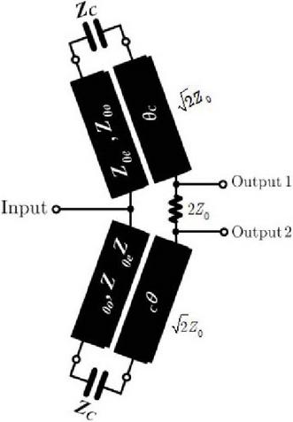
Figure 11 Proposed miniaturized Wilkinson power divider using capacitive-compensated parallel-coupled transmission lines.
3.2 Circuit simulation and results
The schematic model of the proposed miniaturized Wilkinson power divider was implemented in Advanced Design System (ADS) 2022 Update 1 (Keysight Technologies), [34], as illustrated in Fig. 12. The substrate parameters were defined using the MSUB (microstrip substrate) block, including the relative dielectric constant, substrate thickness, conductor thickness, and loss tangent corresponding to the AD260 substrate. The coupled-line sections were modeled using microstrip coupled-line elements (MCLIN), while the single transmission lines were implemented using MLIN (microstrip line) components. The shunt compensation capacitor was realized as a lumped capacitor connected between the open-circuited ends of the coupled-line section. A isolation resistor was placed between the output ports to preserve the inherent isolation property of the conventional Wilkinson topology. S-parameter simulations were performed using the S_Param block in ADS over a frequency range from 0.1 GHz to 6 GHz with a frequency resolution of 1 MHz. All ports were terminated with a reference impedance of to ensure compatibility with standard microwave measurement conditions.
Parametric optimization was conducted to simultaneously adjust the physical dimensions and the compensation capacitance in order to achieve: (i) proper input impedance matching, (ii) equal power division, and (iii) an electrical phase condition of approximately at the design frequency of 3.0 GHz. The optimization was performed using a combination of parameter sweep, manual tuning, and iterative adjustment to achieve the desired matching, power division, and phase response at 3.0 GHz.
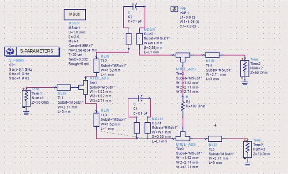
Figure 12 ADS schematic of the proposed Wilkinson power divider including substrate definition, coupled-line sections, and compensation capacitor.
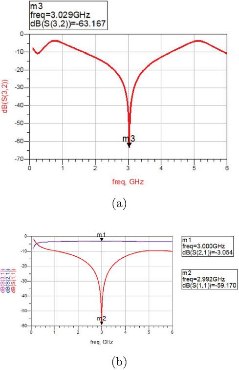
Figure 13 Simulated S-parameters of the proposed Wilkinson power divider. (a) Isolation characteristic. (b) Return loss and insertion loss.
The simulated scattering parameters of the optimized design are presented in Fig. 13. At the center frequency of 3.0 GHz, the proposed power divider exhibits an insertion loss of approximately dB, which is very close to the theoretical value of dB for ideal equal power division.
The input return loss is better than dB, indicating excellent impedance matching at the design frequency. Moreover, the isolation between the output ports () is better than dB, confirming that the compensated coupled-line structure successfully maintains the isolation performance of the conventional Wilkinson divider despite the reduced physical length.
3.3 Fabrication and measurement procedure
After circuit and electromagnetic (EM) optimization, the final layout was exported from ADS and fabricated using a standard printed circuit board (PCB) photolithography process. The microstrip patterns were etched on FR4 and AD260 substrates. For clarity, the AD260 substrate used in this work has a relative dielectric constant of , a thickness of 1 mm, and a copper thickness of 35 m.
The compensation capacitor was implemented using a commercial surface-mount chip capacitor soldered between the open ends of the parallel-coupled microstrip lines. The chip capacitor used in the prototype has a tolerance of , which may introduce slight variations in the measured results compared with the simulated values.
A surface-mount chip resistor was used to realize the isolation resistor between the two output ports, thereby preserving the intrinsic isolation characteristic of the Wilkinson topology.
Standard SMA (Sub-miniature version A) connectors were mounted at the input and output ports. Particular care was taken during soldering to minimize parasitic inductance and excess conductor loss at the feed transitions, which may otherwise degrade the high-frequency performance.
The fabricated prototype was characterized using a calibrated vector network analyzer (VNA) over the frequency range of 2.0–6.0 GHz. Prior to measurement, a full two-port Short-Open-Load-Through (SOLT) calibration was performed. The calibration reference plane was established at the SMA connector interfaces to eliminate systematic errors caused by cables, connectors, and adapters.
The measured S-parameters were subsequently compared with the circuit-level and EM simulation results. Any minor discrepancies are attributed to fabrication tolerances, variations in substrate dielectric properties, and parasitic effects of lumped components.
Table 4 Design parameters of the proposed miniaturized Wilkinson power divider implemented on AD260 substrate at 3.0 GHz
| Substrate Parameters (AD260) | |||
| mm | mm | GHz | |
| Coupled-Line Design Parameters | |||
| Coupling factor | |||
| dB | |||
| Physical dimensions | mm, mm, mm | ||
| Optimized Values | |||
| Compensation capacitor | pF | ||
| Optimized dimensions | mm, mm, mm | ||
| Simulated S-Parameters at 3.0 GHz | |||
| dB | dB | dB | |
| Operational bandwidth: 2–6 GHz | |||
Table 4 summarizes the key design parameters of the proposed miniaturized Wilkinson power divider implemented on the AD260 substrate at 3.0 GHz. The table presents the initial coupled-line parameters, optimized physical dimensions, and the selected compensation capacitance. It can be observed that the coupling factor of dB results in optimized even- and odd-mode impedances that satisfy the impedance transformation requirement of approximately . After compensation, the electrical length is shortened from the conventional quarter-wavelength condition, while maintaining excellent impedance matching and isolation performance.
The fabricated prototype of the proposed miniaturized Wilkinson power divider is shown in Fig. 14. The microstrip layout was implemented on the AD260 substrate with a three-port configuration and integrated parallel-coupled transmission-line sections. The overall physical dimensions of the fabricated circuit are approximately mm2, corresponding to a size reduction of about 22% compared with a conventional quarter-wavelength Wilkinson power divider operating at the same frequency. Surface-mount compensation capacitors were soldered between the open-circuited ends of the coupled-line structure, while a isolation resistor was mounted between the output ports to preserve the Wilkinson topology. The experimental realization confirms that the proposed capacitive-compensated coupled-line structure can be implemented using standard single-layer PCB fabrication without requiring multilayer processing or three-dimensional integration. The compact planar configuration makes the design suitable for integration into modern RF front-end modules.
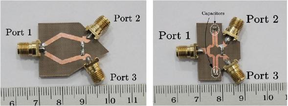
Figure 14 Fabricated prototype of the proposed miniaturized Wilkinson power divider.
4 RESULTS AND DISCUSSION
The measured S-parameters of the fabricated prototypes, including both the proposed miniaturized design and the conventional quarter-wavelength Wilkinson power divider, were obtained using a calibrated vector network analyzer (Keysight S5065) over the frequency range of 2.0–6.0 GHz.
4.1 S-parameter performance
Figure 15 compares the measured S-parameters of the proposed and conventional structures. At the design frequency of 3.0 GHz, the proposed miniaturized power divider exhibits and of approximately dB, which are very close to the ideal dB value for equal power division. The slight additional loss compared to simulation is attributed to dielectric loss of the AD260 substrate, conductor loss, soldering parasitics, and SMA connector effects. The measured input return loss is better than 20 dB at 3.0 GHz, indicating good impedance matching performance. Although the simulated return loss was below dB, the measured result reflects practical implementation conditions. Compared with the conventional design, the proposed structure maintains comparable power division characteristics, while achieving a significant size reduction of approximately 22%. This confirms that the capacitive-compensated coupled-line section effectively replaces the conventional quarter-wavelength transmission line without degrading fundamental performance.
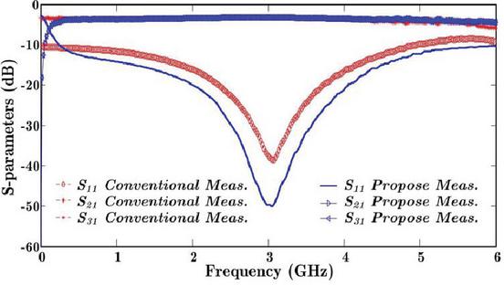
Figure 15 Measured S-parameters of the proposed and conventional Wilkinson power dividers over the frequency range of 2.0–6.0 GHz.
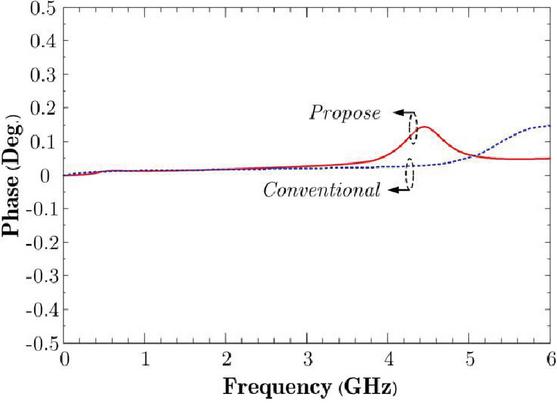
Figure 16 Measured phase difference between output ports of the proposed and conventional Wilkinson power dividers.
4.2 Phase difference analysis
In addition to amplitude characteristics, the phase response between the two output ports was also investigated. Figure 16 shows the measured phase difference between the output ports for both the proposed and conventional structures. Near the operating frequency of 3.0 GHz, the proposed design maintains a phase condition very close to the desired relationship, demonstrating that the capacitive compensation successfully mitigates the even–odd mode phase velocity imbalance inherent in microstrip coupled-line structures. Across the wider frequency range of 2.0–6.0 GHz, the proposed structure exhibits a stable and controlled phase variation, while preserving performance comparable to the conventional topology. This confirms that the shortened coupled-line section provides accurate electrical-length equivalence to the transmission line. Overall, good agreement between theoretical analysis, simulation, and measurement is observed. The proposed capacitive-compensated parallel-coupled transmission-line structure achieves accurate impedance transformation, controlled phase response, and approximately 22% size reduction, making it suitable for compact RF front-end applications.
Table 5 Performance comparison with representative compact Wilkinson power dividers
| Ref. | Frequency (GHz) | Technique | Key Feature | Limitation |
| [1] | 3.0 | Resonator-based | Harmonic suppression | Complex structure |
| [3] | 2.0 | Capacitive loading | Compact design | Lumped elements required |
| [4] | 2.4 | Active inductors | Size reduction | High complexity |
| [11] | 2.45 | Stub-based | Compact structure | Limited flexibility |
| [6] | 0.9 | DGS / Fractal | Size reduction | Ground modification required |
| This work | 3.0 | Coupled-line + capacitor | Compact + integrated phase | Simple planar structure |
4.3 Discussion
For a clearer quantitative comparison, the measured performance of the conventional quarter-wavelength Wilkinson power divider and the proposed miniaturized design is summarized as follows. At the design frequency of 3.0 GHz, the conventional structure exhibits an input return loss of approximately dB, whereas the proposed design achieves an improved return loss of about dB. This indicates that the capacitive-compensated coupled-line section provides more accurate impedance transformation at the operating frequency. Regarding power division performance, the conventional divider shows and of approximately dB, while the proposed structure achieves dB for both output ports. The difference between the two designs is negligible (less than 0.02 dB), confirming that the miniaturization technique does not degrade equal power division characteristics. In terms of physical dimensions, the conventional design occupies an area of mm2, whereas the proposed structure measures mm2. This corresponds to an overall footprint reduction of approximately 22%. The size reduction is achieved without compromising impedance matching or insertion-loss performance. These results demonstrate that the proposed capacitive-compensated parallel-coupled transmission-line structure successfully replaces the conventional quarter-wavelength section, providing improved matching performance together with significant circuit miniaturization. It should be noted that the potential coupling effects between adjacent microstrip lines were considered in the design. The spacing between transmission lines was carefully optimized to minimize unintended parasitic coupling. Furthermore, full-wave EM simulation inherently accounts for these coupling effects. The good agreement between simulation and measurement confirms that such effects have negligible impact on the overall performance.
The performance of the coupled microstrip line used in the proposed design can be compared with that of a conventional quarter-wavelength transmission line. In the proposed structure, the phase response is achieved through the combined effect of electromagnetic coupling and capacitive compensation, enabling the shortened transmission line to approximate the required phase shift at the design frequency. In terms of insertion loss, the coupled-line section with a lumped capacitor may introduce slightly higher loss compared to a conventional uniform transmission line due to additional coupling effects and component parasitics. However, both simulated and measured results indicate that the insertion loss remains close to the ideal value, demonstrating that the additional loss is minimal. These results confirm that the proposed approach provides an effective trade-off between size reduction and electrical performance, making it suitable for compact RF and microwave circuit applications.
Table 5 compares the proposed design with representative compact Wilkinson power dividers reported in the literature. Various techniques such as resonator-based structures, capacitive loading, DGS, and stub-based configurations have been widely used to achieve size reduction. However, these approaches often introduce additional structural complexity or require modifications to the ground plane or active components. In contrast, the proposed design employs a capacitive-compensated coupled-line structure, which enables size reduction through phase integration while maintaining a simple planar configuration. This makes the proposed design more suitable for practical implementation in RF and microwave circuits.
5 CONCLUSIONS
A compact Wilkinson power divider employing a capacitive-compensated parallel-coupled microstrip transmission-line section has been presented. The conventional quarter-wavelength transmission line was replaced by a shortened coupled-line structure integrated with a shunt compensation capacitor, enabling simultaneous impedance transformation and precise phase control at 3.0 GHz. Based on even–odd mode analysis, closed-form expressions were derived to determine the required compensation capacitance and shortened electrical length. Parametric investigation further revealed an approximately linear relationship between the coupling factor and both the compensation capacitance and phase response, providing practical design guidelines within the range of to dB.
The proposed divider was designed using Advanced Design System (ADS), fabricated on an AD260 substrate, and experimentally characterized using a calibrated vector network analyzer over the frequency range of 2.0–6.0 GHz. At the operating frequency of 3.0 GHz, the measured and were approximately dB, the return loss exceeded 20 dB, and the isolation was better than 30 dB. These results show good agreement with simulation and confirm accurate impedance transformation and phase compensation. Compared with the conventional quarter-wavelength Wilkinson power divider, the proposed structure achieves approximately 22% reduction in physical area while preserving balanced power division and isolation characteristics. The fully planar configuration, together with the simple capacitive compensation technique, makes the design suitable for compact RF and microwave front-end applications.
ACKNOWLEDGMENT
This project is financially supported by Mahasarakham University. The authors would like to express their sincere gratitude to the National Electronics and Computer Technology Center (NECTEC), Thailand, for Advanced Design System (ADS) software used in this research.
REFERENCES
[1] M. S. Imani and M. Hayati, “Compact Wilkinson power divider with extensive suppression of harmonics using, a combination of trapezoidal, circular and rectangular resonators,” AEU-Int. J. Electron. Commun., vol. 139, p. 153935, 2021.
[2] K. Nishikawa, T. Tokumitsu, and I. Toyoda, “Miniaturized Wilkinson power divider using three-dimensional MMIC technology,” IEEE Microw. Guided Wave Lett., vol. 6, no. 10, pp. 372–374, 1996.
[3] M. C. Scardelletti, G. E. Ponchak, and T. M. Weller, “Miniaturized Wilkinson power dividers utilizing capacitive loading,” IEEE Microw. Wireless Compon. Lett., vol. 12, no. 1, pp. 6–8, 2002.
[4] L.-H. Lu, Y.-T. Liao, and C.-R. Wu, “A miniaturized Wilkinson power divider with CMOS active inductors,” IEEE Microw. Wireless Compon. Lett., vol. 15, no. 11, pp. 775–777, 2005.
[5] D. K. Pandey and S. Sanyal, “Miniaturized Wilkinson power divider with higher harmonic suppression,” in Proc. Int. Conf. Electromagn. Interference Compat., pp. 37–40, 2008.
[6] N. Gupta, P. Ghosh, and M. Toppo, “A miniaturized Wilkinson power divider using DGS and fractal structure for GSM application,” Prog. Electromagn. Res. Lett., vol. 27, pp. 25–31, 2011.
[7] A. S. Dhahir, H. Abbasi, and F. Shama, “Wilkinson power divider design utilizing trapezoidal and rectangular resonators to suppress harmonics,” Electromagnetics, pp. 1–15, 2025.
[8] M. Chongcheawchamnan, N. Siripon, and I. D. Robertson, “Design and performance of improved lumped-distributed Wilkinson divider topology,” Electron. Lett., vol. 37, no. 8, pp. 501–503, 2001.
[9] Y. Nakayama and H. Hayashi, “A miniaturized lumped-element in-phase power divider with a simple layout,” in Proc. UKSim-AMSS Int. Conf. Comput. Model. Simul., pp. 595–598, 2014.
[10] S. Shamsinejad, M. Soleimani, and N. Komjani, “Novel miniaturized Wilkinson power divider for 3G mobile receivers,” in Proc. Int. Conf. Microw. Millim. Wave Technol., vol. 3, pp. 1268–1270, 2008.
[11] H. P. Phan, T. P. Vuong, T. T. Nguyen, M. H. Luong, Y. Iitsuka, and M. H. Hoang, “Simple miniaturized Wilkinson power divider using a compact stub structure,” in Proc. Int. Conf. Adv. Technol. Commun. (ATC), pp. 168–171, 2015.
[12] S. Roshani and S. Roshani, “Design of a compact LPF and a miniaturized Wilkinson power divider using aperiodic stubs with harmonic suppression for wireless applications,” Wireless Netw., vol. 26, no. 2, pp. 1493–1501, 2020.
[13] A. N. Bazaz, H. Abbasi, and F. Shama, “Harmonics eliminated Wilkinson power divider with modified stepped-impedance and radial units,” J. Electromagn. Waves Appl., pp. 1–13, 2025.
[14] Y. C. Leong and S. Weinreb, “Novel technique of phase velocity equalization for microstrip coupled-line phase shifters,” in Proc. IEEE MTT-S Int. Microw. Symp. Dig., vol. 3, pp. 1453–1456, 2000.
[15] H. R. Ahn, K. Min, D. Kang, S. Hong, and B. Kim, “Coupling-compensated 180 phase shift coupled-line filters terminated in arbitrary impedances,” in Proc. Asia-Pacific Microw. Conf., pp. 649–652, 2006.
[16] M. Ould-Elhassen, M. Mabrouk, A. Ghazel, and P. Benech, “Differential tunable phase shifter,” in Proc. IEEE Int. Symp. Phased Array Syst. Technol., pp. 97–101, 2013.
[17] T. A. Abir, “A broadband microstrip Schiffman phase shifter with load and source impedance matching,” master’s thesis, Texas A&M University–Kingsville, 2014.
[18] Y. Wu, S. Zhou, X. Shen, and Y. Liu, “A compact and miniaturized broadband phase shifter using coupled-lines,” Applied Computational Electromagnetics Society (ACES) Journal, pp. 806–811, 2016.
[19] A. Podell, “A high directivity microstrip coupler technique,” in Proc. IEEE MTT-S Int. Microw. Symp., pp. 33–36, 1970.
[20] D. D. Paolino, “MIC overlay coupler design using spectral domain techniques,” IEEE Trans. Microw. Theory Tech., vol. 26, no. 9, pp. 646–649, 1978.
[21] L. Su, T. Itoh, and J. Rivera, “Design of an overlay directional coupler by a full-wave analysis,” IEEE Trans. Microw. Theory Tech., vol. 31, no. 12, pp. 1017–1022, 1983.
[22] S. Uysal and H. Aghvami, “Synthesis, design, and construction of ultra-wide-band nonuniform quadrature directional couplers in inhomogeneous media,” IEEE Trans. Microw. Theory Tech., vol. 37, no. 6, pp. 969–976, 1989.
[23] J. L. Klein and K. Chang, “Optimum dielectric overlay thickness for equal even- and odd-mode phase velocities in coupled microstrip circuits,” Electron. Lett., vol. 26, no. 5, pp. 274–276, 1990.
[24] B. Sheleg and B. E. Spielman, “Broad-band directional couplers using microstrip with dielectric overlays,” IEEE Trans. Microw. Theory Tech., vol. 22, no. 12, pp. 1216–1220, 2003.
[25] S. L. March, “Phase velocity compensation in parallel-coupled microstrip,” in Proc. IEEE MTT-S Int. Microw. Symp. Dig., pp. 410–412, 1982.
[26] M. Dydyk, “Accurate design of microstrip directional couplers with capacitive compensation,” in Proc. IEEE MTT-S Int. Microw. Symp. Dig., pp. 581–584, 1990.
[27] D. Kajfez, “Raise coupler directivity with lumped compensation,” Microwaves, pp. 64–70, 1978.
[28] I. J. Bahl, “Capacitively compensated high performance parallel coupled microstrip filters,” in Proc. IEEE MTT-S Int. Microw. Symp. Dig., pp. 679–682, 1989.
[29] R. Phromloungsri, M. Chongcheawchamnan, and I. D. Robertson, “Inductively compensated parallel coupled microstrip lines and their applications,” IEEE Trans. Microw. Theory Tech., vol. 54, no. 9, pp. 3571–3582, 2006.
[30] R. Phromloungsri, V. Chamnanphrai, and M. Chongcheawchamnan, “Design high-directivity parallel-coupled lines using quadrupled inductive-compensated technique,” in Proc. Asia-Pacific Microw. Conf., pp. 1380–1383, 2006.
[31] S. Lee and Y. Lee, “An inductor-loaded microstrip directional coupler for directivity enhancement,” IEEE Microw. Wireless Compon. Lett., vol. 19, no. 6, pp. 362–364, 2009.
[32] S. Lee and Y. Lee, “A design method for microstrip directional couplers loaded with shunt inductors for directivity enhancement,” IEEE Trans. Microw. Theory Tech., vol. 58, no. 4, pp. 994–1002, 2010.
[33] S. Sonasang and N. Angkawisittpan, “Design of microstrip parallel-coupled lines with high directivity using symmetric-centered inductors,” Applied Computational Electromagnetics Society (ACES) Journal, pp. 657–663, 2021.
[34] Keysight Technologies, “Advanced Design System (ADS), Version 2022 Update 1,” Keysight Technologies, Santa Rosa, CA, USA, 2022.
BIOGRAPHIES

Thanapat Chiawchanwattana was born in Udorn Thani, Thailand. He received the B.Eng. (Computer Engineering) from Khon Kaen University, in 1999, M.Eng. in Computer Engineering from Khon Kaen University (KKU), in 2006, Thailand. He is currently pursuing a Ph.D. in Electrical and Computer Engineering at the Faculty of Engineering, Mahasarakham University, Thailand. Currently, he is working in the Department of Computer and Communication Engineering at Udon Thani Rajabhat University. His research interests include IoT/Automation system and RF/Microwave Circuits design.

Ravee Phomloungsri was born in Khon Kaen, Thailand. He received the B.Sc. degree in Applied Physics (Solid-State Electronics) from King Mongkut’s Institute of Technology Ladkrabang (KMITL), Thailand, in 1992, and graduated with M. Eng and D.Eng. in Electrical Engineering (Telecommunications) from Mahanakorn University of Technology (MUT), Thailand, in 2001, and 2006, respectively.
From 1992 to 2009, he was a Lecturer with the Department of Telecommunication Engineering, MUT. He is currently an Associate Professor with the Department of Computer and Communication Engineering, Udon Thani Rajabhat University, Thailand. His research interests include IoT and automation systems, as well as RF and microwave circuit design.

Somkuan Srisawat was born in Nongbua Lamphu, Thailand. He received the B.Eng. degree in Electronics Engineering from Udon Thani Rajabhat University, Thailand, in 2011, and the M.Eng. degree in Electrical and Computer Engineering from Mahasarakham University (MSU), Thailand, in 2019.
He is currently with the Department of Computer and Communication Engineering, Udon Thani Rajabhat University, Thailand. His research interests include IoT and automation systems, as well as RF and microwave circuit design.

Niwat Angkawisittpan was born in Khon Kaen, Thailand. He received the B.Eng. degree in Electrical Engineering (Hons.) from Khon Kaen University, Thailand, in 1997, the M.Sc. degree in Electrical and Computer Engineering from Purdue University, Indiana, USA, in 2003, and the Ph.D. degree in Electrical Engineering from the University of Massachusetts Lowell, MA, USA, in 2009.
Since 2009, he has been with the Research Unit for Electrical and Computer Engineering Technology (RECENT), Faculty of Engineering, Mahasarakham University, Maha Sarakham, Thailand, where he is currently an Associate Professor. He has authored or co-authored numerous journal and conference papers. His research interests include artificial intelligence, machine learning, image processing, neural networks, compact microstrip devices, metamaterial applications for RF and microwave circuits, and electromagnetic material characterization.

Sivarit Sultornsanee is an Associate Professor in the College of Engineering at Northeastern University, where he previously served as Data Analytics Engineering Program Coordinator. He earned his M.S. in Computer Engineering from the University of Massachusetts Lowell and his Ph.D. in Interdisciplinary Engineering from Northeastern University. He provides strategic leadership in analytics education and industry collaboration, advancing the application of artificial intelligence, machine learning, and IoT to healthcare, intelligent systems, and smart industry transformation.
ACES JOURNAL, Vol. 41, No. 5, 457–472
DOI: 10.13052/2026.ACES.J.410508
© 2026 River Publishers