Chemical Bath Deposition of CdZnS as Buffer Layer in CIGS Solar Cell
Yuming Xue*, Xinyu Wang, Liming Zhang, Shipeng Zhang, Lang Wang and Hang Sun
Tianjin Key Laboratory of Film Electronic & Communication Devices, School of Integrated Circuit Science and Engineering, Tianjin University of Technology, Tianjin 300384, China
E-mail: orwellx@tjut.edu.cn
*Corresponding Author
Received 18 August 2021; Accepted 02 September 2021; Publication 09 November 2021
Abstract
CdZnS thin films were deposited on glass substrates by chemical bath deposition (CBD). The effect of ZnSO solution concentration on the properties of the thin films was analyzed. The concentration of ZnSO solution affects the deposition rate of CdZnS thin films. When the deposition rate is low, CdZnS cubic crystal phase is formed. The surface morphology of hexagonal CdZnS thin films is denser than that of cubic phase, the lattice mismatch rate of cubic phase CdZnS thin films and CIGS is lower, only 0.56%, the interfacial state density is lower. SCAPS software was used to simulate the performance of the buffer layer and the conversion efficiency of the cubic phase CdZnS buffer layer in CIGS Solar Cell was up to 23.50%. Based on the EDS results, the functional relationship between the contents of Zn and Cd in the films and the bandgap content was deduced.
Keywords: CBD (chemical bath deposition), Zinc sulfate concentration, CIGS solar cell.
Introduction
CdS, the II-VI group compound, is an n-type semiconductor material [1] with a bandgap of 2.45 eV. CdS exhibit good transmittance in the visible range, so it is suitable as a buffer layer for heterojunction solar cells [2]. Several methods are used for preparing CdS films, such as thermal evaporation [3], atomic layer deposition [4], and chemical bath deposition [5]. The CBD method is used to deposit the buffer layer film (approximately 50 nm in thickness) uniformly and densely. As the buffer layer of copper indium gallium selenide (CIGS) solar cells, CdS can reduce the bandgap discrepancy between CIGS (1.02–1.67 eV) and ZnO (3.2 eV), thereby improving the photoelectric conversion efficiency of solar cells. The American CIGS film developer Stion has achieved a conversion efficiency of 23.2% for 20 cm 20 cm CIGS cells [5]. However, CdS is highly toxic and environmentally hazardous, and its small optical bandgap hinders the absorption of short-wavelength radiation [6]. Researchers have found that Cd can be replaced by adding Mg or Zn. ZnS, an n-type semiconductor [6] compound with an optical band gap of 3.71 eV, has good short-wave transmittance and is both non-toxic and environmentally friendly; It is widely considered a replacement for CdS. However, ZnS exhibits poor lattice matching with CIGS thin-film solar cells and significantly high resistivity, which seriously affects the efficiency of thin-film solar cells. Therefore, it is necessary to manufacture CdZnS thin-film semiconductor materials. In this study, the ZnSO solution provides Zn to reduce the Cd content in the film and finally form a film of CdZnS. The CdZnS film has two crystal phases: the cubic phase and the hexagonal phase. Different deposition conditions can be used to prepare CdZnS films containing either or both of these two phases. Vidhya and Velumani used microwave-activated CBD (MW-CBD) to prepare a hexagonal-lattice CdZnS film with a bandgap of 2.6 eV [7]. In 2019, Kaur et al. also reported the formation of CdZnS thin films with mixed crystal phases through an ion-by-ion process. The formation of different crystal phases in CdZnS films depends on the solution temperature, pH, and reactant concentration. The concentration of the reactants has the most significant influence on the type of crystal phase formation. Therefore, in this study, the CBD method is used to prepare CdZnS thin films. The effect of Zn concentration on the morphology, structural characteristics, and thin-film optical properties is analyzed. Although studies on the concentration of Zn on CdZnS films have been widely reported, the Zn sources most widely used are Zn(Ac), ZnCl, or Zn(CHCO. Few researchers have studied the effect of ZnSO on film. Increasing the amount of ZnSO solution will gradually increase the position of the diffraction peak. This is an essential basis for the transition of CdZnS from the hexagonal phase to the cubic phase. In order to improve the efficiency of CIGS, we can try to reduce the lattice mismatch ratio of heterojunction and reduce the interfacial state density.
In this study, we analyzed the effects of ZnSO concentration on the morphology, structural characteristics, and optical properties of CdZnS: films and the matching of CdZnS and CIGS with different crystal phases and the density of interfacial states. The aim is to improve the performance of the optical and electrical morphologies of the film.
1 Method
CdZnS thin films were deposited on glass substrates by chemical bath deposition method to make the buffer layer without pinholes and completely cover the surface of CIGS thin films to avoid damage caused by subsequent processes such as sputtering ZnO. In the reaction, ZnSO provides Zn, CdSO provides Cd, NH3*H2O forms complex with Zn and Cd as a complexing agent, and SC(NH) provides anion: S to participate in the reaction.
As a buffer, (NH)SO reduces the release rate of metal ions and promotes the formation of CdZnS films. When the ionic product is more excellent than the solubility product ofCdZnS, or (8) reaction occurs in the solution to generate precipitation, forming a colloidal body; Or the reaction (8) occurs on the lining bottom and the surface of the container wall to form a film. Therefore, in depositing CdZnS film by the CBD method, a homogeneity reaction Homogeneous reaction in the solution and a heterogeneous reaction occurs on the substrate and the surface of the container wall. These two competing chemical reactions. The homogeneity reaction will form many colloidal particles in the solution, which will deteriorate the performance of CdZnS films. Therefore, the deposition of high-quality CdZnS films must be managed to inhibit the occurrence of homogeneous reactions.
The chemical equations used in the experiment is as follows:
Hydrolysis ammonia
| (1) |
CdSO provides Cd to react with ammonia to form complex ions
| (2) | |
| (3) |
ZnSO provides Zn to react with ammonia to form complex ions:
| (4) | |
| (5) |
Thiourea reacts with OH to form S
| (6) | |
| (7) |
The complexions of zinc and cadmium react with S formed by OH from the hydrolysis of thiourea and ammonia to produce CdZnS:
| (8) |
2 Experimental
2.1 Film Preparation
CdZnS films were prepared on glass substrates via the CBD method. The experimental temperature is 85C. The glass substrate size is 3 cm 2 cm. The glass substrates were cleaned with detergent, followed by sequentially washing via ultrasonic treatment in deionized water. A solution of CdSO (0.05 M), (NH)SO (0.1 M), and ZnSO (0.01 M, 0.015 M, 0.020 M, 0.025 M and 0.030 M) with an appropriate amount of deionized water is prepared by stirring well with a glass rod and placed in a water bath kettle. Finally, SC(NH) (1 M) and NHHO (13.33 M) were added to each of the five beakers. The presence of Cd, Zn, and S in the solution will precipitate rapidly and affect the growth of the film. Therefore, in the CBD method, complexing agent (NH*HO) and buffer ((NH)SO) are generally added to reduce the release rate of metal ions, and NH reacts with Cd, Zn to form a stable complex of cadmium and zinc, thus effectively controlling the deposition rate of the film and improving the growth quality of the film.
The reaction solution is stirred every 5 min during the experiment. After the experiment, the substrate was cleaned with deionized water and dried for further use.
Characterization of CdZnS Film
A Rigaku D/max-RB X-ray diffractometer (XRD) is used to analyze the crystallization and structure of the films. A Cu target is used, the sample scanning range is 10–70, the step size is 0.02, the voltage is 40 kV, and the current is 200 mA. The film’s surface morphology is analyzed using a scanning electron microscope (SEM 460L03040702), and the composition and elemental content of the film is analyzed by an energy-dispersive spectrometer (EDS 460L03040702). Spectrophotometer (UV–Vis–NIR TP720) is used to test the absorption transmittance of the film in the wavelength range 300–800 nm and calculate the bandgap.
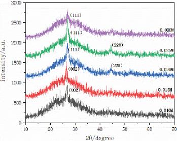
Figure 1 XRD patterns of Cd1-xZnxS film.
3 Results
3.1 X-Ray Diffraction Analysis
Figure 1 shows the XRD patterns of CdZnS films deposited with different concentrations of ZnSO. Table 1 shows the position of the diffraction peak and crystal phase. It can be seen that when the concentration of ZnSO is 0.010 M and 0.015 M, the diffraction peak grows preferentially in (002) direction, and the diffraction peak position is around , slightly behind that of CdS (002) . This is because Zn (0.74 A) is less than Cd (0.97A) [8, 9]. The bond lengths of Cd-S and Zn-S are 0.279 nm and 0.258 nm, respectively [8, 9]. Zn mixes with Cd at the CdS or interstitial position to form CdZnS. When the concentration of ZnSO is 0.020 M, 0.025 M, the diffraction peak grows preferentially at with (111), the diffraction peak appears at with (220). When the concentration of ZnSO is 0.030 M, the diffraction peak (220) disappears, and the intensity of the diffraction peak (111) gradually weakens. Due to the increase of Zn content, the release rate of Cd and Zn ions in the solution is accelerated, leading to the formation of precipitate between Cd complex and Sfaster than the formation rate CdZnS thin film. The concentration of ZnSO gradually shifted to a small Angle from Angle 2 at the diffraction peak position of 0.030 M–0.10 M samples, which indicated that their lattice constants decreased gradually due to the filling vacancy defects and the presence of S in the void position [10].
Table 1 Diffraction peak parameters of ZnSO with different concentrations
| ZnSO(M) | 2 | (h k l) Crystal System |
| 0.010 | 26.8 | (002) |
| 0.015 | 26.6 | (002) |
| 0.020 | 27.21, 44.55 | (111), (220) |
| 0.025 | 27.13, 44.55 | (111), (220) |
| 0.030 | 27.18 | (111) |
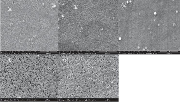
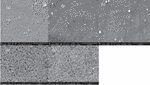
Figure 2 Surface morphology images of CdZnS films prepared with ZnSO4 concentrations of (a) 0.010 M, (b) 0.015 M, (c) 0.020 M, (d) 0.025 M, and (e) 0.030 M.
Surface Morphology
Figures 2(a–e) are the surface morphology images of the CdZnS films with the ZnSO concentrations of 0.010 M, 0.015 M, 0.020 M, 0.025 M, and 0.030 M. It can be seen from the image that when the concentration of ZnSO is 0.015 M, the film has the best density and the tiniest white particles on the surface. The surface density of the hexagonal phase film is better than the cubic phase. When the concentrations of ZnSO are 0.025 M and 0.030 M, the film density gradually decreases, and some holes appear on the surfaces. The hydrolysate of ammonia produces OH, which reacts with a large amount of Zn and Cd in the solution to produce Cd(OH) and Zn(OH), which are deposited on the glass matrix and hinder the formation of the buffer layer film.
EDS and Composition Profile Study
The atomic percentages of S, Zn, and Cd in the CdZnS thin films formed at ZnSO concentrations of 0.010 M, 0.015 M, 0.020 M, 0.025 M, and 0.030 M were measured by EDS, as shown in Table 2, respectively. The ratio of Zn/(ZnCd) concentrations values are 0.481, 0.625, 0.711, 0.751, and 0.899, increases as the concentration of ZnSO increases. As the concentration of ZnSO increases, the concentration of Zn in the solution increases, and a certain amount of Zn(OH) colloidal particles are deposited on the film, which decreases the density of the film.
Table 2 The atomic ratios of Cd, Zn, and S in CdZnS films prepared with different ZnSO concentrations
| C(ZnSO) (M) | S:Zn:Cd |
| 0.010 | 29.82:33.81:36.37 |
| 0.015 | 25.92:49.44:24.65 |
| 0.020 | 22.28:55.27:22.44 |
| 0.025 | 21.80:58.70:19.50 |
| 0.030 | 10.82:80.80:8.38 |
Optical Properties
Bandgap Energies
CdZnS is a direct-bandgap semiconductor [13], and the optical bandgap and absorption coefficient satisfy the Tauc Equation (9):
| (9) |
The absorption coefficient can be calculated using formula (10):
| (10) |
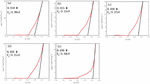
where is the absorption coefficient, E is the optical band gap, h is the photon energy, T is the film transmittance, d is the film thickness, and A is a constant. Using Equation (10) and combining the measured transmittances and thicknesses of the films to calculate , we use the calculated values in Equation (9) to draw an (h)–h scatter diagram. Figures 3(a)–(e) show the optical bandgaps of the CdZnS films made with different ZnSO concentrations. When the ZnSO concentrations are 0.010 M, 0.015 M, 0.020 M, 0.025 M, and 0.030 M, the optical bandgaps of the CdZnS films are 2.99 eV, 3.21 eV, 3.27 eV, 3.31 eV, and 3.58 eV, respectively. As the concentration of ZnSO increases, the optical bandgaps gradually increase, and the trend of the bandgap changes is consistent with that of the ZnSO content, as observed in the EDS profiles.
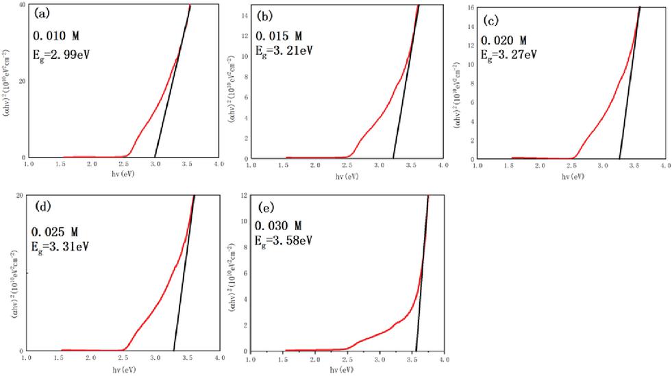
Figure 3 Optical bandgaps of CdZnS films formed with ZnSO concentrations of (a) 0.010 M, (b) 0.015 M, (c) 0.020 M, (d) 0.025 M, and (e) 0.030 M.
Numerical Simulation
In order to prove the feasibility of the CdZnS produced in this experiment as the buffer layer of CIGS solar thin-film cell, the AC-DC characteristics of the thin film cell were simulated by SCAPS software. We have considered the good structure of solar cells based on CIGS (Mo/CIGS/CdS/ZnO). The typical thickness of each layer was obtained from different references and substituted the CdS with the experimental results of CdZnS [13–16]. In the experimental simulation, the illumination condition is 1000 W/m, T 300 K. Defect type is set to Neutral, energy level concerning reference is 0.6, and characteristic energy is 0.1 eV. Other parameters are shown in Table 4. The simulation results are shown in Table 3.
Table 3 Simulation Parameter of the study
| Parameters | CIGS [14–16] | OVC | i-ZnO | CdZnS |
| Thickness (nm) | 1600 | 15 | 80 | Experiment |
| Eg (eV) | 1.15 | 1.45 | 3.4 | Experiment |
| (eV) | 4.5 | 4.5 | 4.55 | 4.45 |
| r | 10 | 10 | 10 | 9 |
| Nc (cm) | 2.0 10 | 2.1 10 | 4.0 10 | 2.1 10 |
| Nv (cm) | 2.0 10 | 2.1 10 | 9.0 10 | 1.7 10 |
| e (cm/Vs) | 100 | 10 | 100 | 50 |
| h (cm/Vs) | 12.5 | 10 | 25 | 20 |
| ND (cm) | – | 1.0 10 | 5.0 10 | 1.0 10 |
| NA (cm) | 5.5 10 | – | – | – |
Table 4 The simulation results
| C(ZnSO) (M) | V(V) | J(mA/cm) | FF% | ETA% |
| 0.010 | 0.7066 | 40.476088 | 81.84 | 23.41 |
| 0.015 | 0.7067 | 40.534166 | 81.88 | 23.45 |
| 0.020 | 0.7067 | 40.545422 | 81.88 | 23.46 |
| 0.025 | 0.7070 | 40.552104 | 81.96 | 23.50 |
| 0.030 | 0.7070 | 40.552462 | 81.95 | 23.50 |
It can be concluded that when the concentration of zinc sulfate is 0.025 M, the conversion efficiency of the cell is higher, reaching 23.50%, and the experimental results can be effectively applied to the actual manufacturing of CIGS solar cells.
4 Discussion
Lattice Mismatches and Interfacial Densities of Heterojunctions
The strict lattice constant matching between the two semiconductors forming the heterojunction is essential for good performance. Lattice mismatch will produce suspension bond, defect state at the interface of two semiconductor materials, introduce interface state, cause trap or recombination center action, and make the properties of heterojunction bad. “Lattice mismatch” is defined as follows:
| (11) |
a and a are the lattice constants of the two materials, respectively (let a2 a1), a (a a)/2 is the average value of the lattice constants of the two materials.
The density of interfacial states is defined as the number of ”hanging bonds” per unit area Nss, which can be derived from the difference of lattice constants
Rough calculation [12]:
| (12) |
If a a (a a)/2, a aa, then: Na/a.
Even a well-matched lattice heterojunction has an interfacial density of 10 cm orders. Table 5 shows the calculation results of lattice mismatch and interfacial density of states.
The CIGS lattice constant (Å) is 5.762 [12], the cubic CdZnS lattice constant (Å) is 5.73, and the hexagonal CdZnS lattice constant (Å) is 4.12 [7]. The lattice constant a(Å) of cubic CdS is 5.818, and the lattice constant a(Å) of hexagonal CdS is 4.141 [12]. The hexagonal lattice mismatch between CdZnS and CIGS in the hexagonal lattice is too large, the interfacial state density is as high as 10, and the lattice mismatch rate is as high as 33.23% [12–16]. Compared with the reference, the cubic CdZnS is more compatible with CIGS than the cubic CdS.
Table 5 The calculation results of lattice mismatch and interfacial density of states
| Interface State | ||
| Heterojunction | Crystal Mismatch% | Density/cm |
| Cubic phase CdZnS/CIGS | 0.56 | 3.3710 |
| Hexagonalphase CdZnS/CIGS | 33.23 | 2.6910 |
| Cubic phase CdS/CIGS | 0.97 [12] | 5.7710 [12] |
| Hexagonal phase CdS/CIGS | 32.74 [12] | 2.8210 [12] |
Relationship Between Element Content and Band Gap in Thin Films
The experimental analysis of EDS data and the film bandgap value data Eg1 obtained using a UV–Vis–NIR spectrophotometer shows that the Zn content of the film is highly correlated with the film bandgap. If the CdZnS compound is expressed as CdZnS, X is the value of Zn/(ZnCd). Through function fitting, the functional relationship between X and the bandgap (E) is obtained. The functional relationship is as follows:
| (13) |
The error between the actual forbidden bandwidth and the function-forbidden bandwidth does not exceed 0.1 eV, proving that the function is reliable. Table 6 shows the Experimental Eg1 and calculated Eg values for each formula value.
Table 6 Experimental E and calculated E values for each formula value
| X Zn/(ZnCd) | E (eV) | E (eV) |
| 0.482 | 2.99 | 3.004 |
| 0.625 | 3.21 | 3.168 |
| 0.711 | 3.27 | 3.282 |
| 0.751 | 3.31 | 3.338 |
| 0.899 | 3.58 | 3.568 |
5 Conclusion
The Zn content in the CdZnS film affects the film flatness, and increasing the concentration of Zn hinders the growth of the film. When the concentration of ZnSO is 0.015 M, the crystallinity and surface density of CdZnS hexagonal films are the best.
When the concentration of ZnSO is 0.020 M, the crystallinity and surface morphology of CdZnS cubic films are the best. The lattice mismatch ratio of CdZnS and CIGS is only 0.56%, and the interfacial density is only 3.37 cm.
EDS shows that as the concentration of ZnSO increases, the film’s Zn/(ZnCd) value gradually increases. The Zn content affects the growth rate. The bandgap value increases as the Zn content increases. Through the experimental analysis of the EDS data and the film bandgap value data, X is determined to be the Zn/(ZnCd) value, and the functional relationship between X and the bandgap (E) is determined as follows:
When the ZnSO concentration is 0.025 M, SCAPS simulation results show that CIGS efficiency is the highest, which is 23.50%
Acknowledgments
The author thanks Professor Yuming Xue and Liming Zhang for directing the experimental papers.
References
[1] M. Isik, H.H. Gullu, S. Delice, M. Parlak, N.M. Gasanly, Structural and temperaturedependent optical properties of thermally evaporated CdS thin films, Mater. Sci. Semicond. Process. 93 (2019) 148–152.
[2] M. Shkir, K.V. Chandekar, A. Khan, et al. Structural, morphological, vibrational, optical, and nonlinear characteristics of spray pyrolyzed CdS thin films: Effect of Gd doping content[J]. Materials Chemistry and Physics, 2020, 255: 123615.
[3] S. Rajathi, R. Vasuki, Thir N. Sankarasubramanian, M. Senthamizhselvi, Preparation and characterization of zinc doped CdS thin films for photovoltaic applications, Adv. Nat. Appl. Sci. 11(8) (2017) 144–152.
[4] M.A. Baghchesara, R. Yousefi, M. Cheraghizade, F. Jamali-Sheini, A. Saáedi, Photocurrent application of Zn-doped CdS nanostructures grown by thermal evaporation method, Ceram. Int. 42(1, B) (2016) 1891–1896.
[5] Y.Z. Hamri, Y. Bourezig, M. Medles, et al. Improved efficiency of Cu(In, Ga)Se2 thin-film solar cells using a buffer layer alternative to CdS[J]. Solar Energy, 2019, (178): 150–156.
[6] Y. Li, H. Lin, J. Zeng, et al. Enhance short-wavelength response of CIGS solar cell by CdSe quantum disks as luminescent down-shifting material[J]. Solar Energy, 2019, 193: 303–308.
[7] R. Zellagui, H. Dehdouh, F. boufelgha, A. Boughelout, T. Sahraoui, D. Chaumont, M. Adnane, Effect of zinc/cadmium proportion in CdS layers deposited by CBDmethod, Int. Multidiscip. Res. J. 9 (2019) 8–12.
[8] Ligang Ma, Xiaoqian Ai, Xiaoshan Wu. “Effect of substrate and Zn doping on the structural, optical and electrical properties of CdS thin films prepared by CBD method”, Journal of Alloys and Compounds, 2017.
[9] Solomon U. Offiah, Ada N.C. Agbogu, Assumpta C. Nwanya, Agnes C. Nkele, Ugochi K. Chime, B. T. Sone et al., Influence of cadmium precursor concentrations on the structural, optical, and electrochemical impedance properties of CdZnS thin films, Vacuum 160 (2019) 246–254.
[10] O. De Melo, L. Hernandez, O. Zelaya-Angel, et al. Low resistivity cubic phase CdS films by chemical bath deposition technique [J]. Appl. Phys. Lett., 1994, 65(10):1278–1280.
[11] Yuli-Sheng. Physics of semiconductor heterojunction [M]. Beijing: Science Press, 1990.
[12] Wei Guo, Yuming Xue, Yong Gu. Influence of solution PH value on structural properties of CdS thin films. Journal of Optoelectronics Laser Vol. 24, No. 11 November 2013.
[13] F.T. Munna, V. Selvanathan, K. Sobayel, et al. Diluted chemical bath deposition of CdZnS as prospective buffer layer in CIGS solar cell[J]. Ceramics International, 2020.
[14] K. Sobayel et al., A comprehensive defect study of tungsten disulfide (WS2) as electron transport layer in perovskite solar cells by numerical simulation, Results in Physics 12 (2019) 1097–1103.
[15] K. Sobayel, et al., Efficiency enhancement of CIGS solar cell by WS2 as window layer through Sol’s numerical modeling tool. Energy 207 (2020) 479–485.
[16] Y. Li, H. Lin, J. Zeng, et al. Enhance short-wavelength response of CIGS solar cell by CdSe quantum disks as luminescent down-shifting material[J]. Solar Energy, 2019, 193: 303–308.
Biographies

Yuming Xue is an associate Professor, School of Integrated Circuit Science and Engineering, Tianjin University of Technology, Tianjin, China. He received PhD degree in Microelectronics and Solid State Electronics. He has been engaged in research on thin film semiconductor materials and devices for 21 years. Deposit thin films by the techniques of co-evaporation, sputtering & selenizing; Deposition, CBD (chemical bath deposition), rf magnetron sputtering and DC magnetron sputtering. Study structural, optical, electrical properties of thin films by many kinds of measurements: XRD, Raman, XRF, EDX, SIMS, SEM, XPS, Hall, HR-optical microscope, Step Profilometer, Infrared Absorption Spectrometry, Spectrophotometry, I-V curve of the solar cells,QE and FTIR. Deposit and research on all thin films made of CIGS thin film solar cell (from Mo back contacts, CIGS absorber layers with OVC surface layer, CdS and Cd(Mg)S) buffer layers, ZnO and ZnSe window layers and ZnO:Al transparent conductive layers to Ni/Al electrodes).

Xinyu Wang (1995–), female, born in Xianyang, Shaanxi province, China. In the fall of 2014, she entered Tianjin University of Technology, majoring in integrated circuits and Integrated Systems, and received her bachelor’s degree in June 2018.
Since autumn 2019, She has been studying for master’s degree in Integrated circuit Engineering in Tianjin Key Laboratory of Film Electronic & Communication Devices, School of Integrated Circuit Science and Engineering, Tianjin University of Technology, Tianjin University of Technology.
Research direction: CIGS thin film solar cell buffer.

Liming Zhang, male, from Henan province, China. In 2018, he was admitted to school of Integrated Circuit Science and Engineering, Tianjin University of Technology. Tianjin Key Laboratory of Thin Film Electronics and Communication Devices, School of Integrated Circuit Science and Engineering, Tianjin University of Technology, Master’s degree in 2020.CIGS buffer layer CdZnS material is studied. CdZnS buffer layer was prepared by water bath method to replace CdS to reduce environmental pollution. XRD, SEM and other methods were used to characterize the properties of the film, and the electrochemical properties were studied.

Shipeng Zhang (1997–), male, born in Huai’an, Jiangsu. Master of integrated circuit engineering, School of School of Integrated Circuit Science and Engineering, Tianjin University of Technology. In the fall of 2015, he entered Nantong University, majoring in Microelectronics Science and Engineering, and received his bachelor’s degree in the summer of 2019. In the fall of 2019, He entered the School of Integrated Circuit Science and Engineering of Tianjin University of Technology to pursue his master degree in integrated circuit engineering. The buffer material of solar cell was studied by chemical bath deposition.

Lang Wang (1996–), male, born in Datong, Shanxi provence, China. In the fall of 2019, he entered the School of Integrated Circuit Science and Engineering of Tianjin University of Technology to study for a master’s degree in Integrated circuit Engineering. He studied optoelectronic Information Science and Engineering in Tianjin University of Technology as an undergraduate. The research direction is to prepare (S, O, Zn) materials by chemical bath deposition to replace CdS as the buffer layer of solar thin film cells, and improve the conversion efficiency of solar cells.

Hang Sun (1997–), male, born in Heilongjiang provence, China. In 2019, He studied for a Master’s degree in Integrated Circuit Engineering at School of Integrated Circuit Science and Engineering. In the summer of 2018, he received his bachelor’s degree in Integrated Circuit Design and Integrated System from Tianjin University of Technology. Now the main research is solar film cells.(S, O, Zn) material is used to replace the buffer layer CdS of the CIGS thin film solar cell buffer. In order to improve the conversion efficiency of the solar cell.
Distributed Generation & Alternative Energy Journal, Vol. 37_2, 401–418.
doi: 10.13052/dgaej2156-3306.37216
© 2021 River Publishers