Analysis of Dual Input Buck-Boost Converter for Solar PV Integration with Wireless Electric Vehicle Charger
Kuditi Kamalapathi*, Ponugothu Srinivasa Rao Nayak and Vipul Kumar Tyagi
Department of Electrical and Electronics Engineering, National Institute of Technology Tiruchirappalli, Tamil Nadu, India
E-mail: kamal.kuditi@gmail.com
*Corresponding Author
Received 02 April 2021; Accepted 22 June 2021; Publication 27 August 2021
Abstract
Investigation of on-board renewable solar PV and wireless EV charging station integration is studied in this paper. Integration of on-board solar PV power with EV charger power will reduce the stress on the grid without the need for extra ground for solar plant installation. A dual-input buck-boost converter (DIBBC) is used to integrate the two power sources and charge the EV battery. A small-signal model of the converter is used to design the controller for three switches of the DIBBC. The simulation model of the integrated solar PV system and wireless power transfer (WPT) system is designed for charging a battery of 120V/165Ah at 130V. The hardware prototype of the proposed EV battery charging system is designed for 1.5kW to verify the simulation results. WPT system is developed for circular spiral-shaped coils, which are series-series compensated for 85kHz resonance frequency. Solar PV is replaced by a solar simulator programmed to operate with the same specifications used in the simulation. Results and analysis of the DIBBC based charger with charging voltage 130V showed higher efficiency up to 92% when both the sources are supplying power to DIBBC. The proposed charging system gives better efficiency with higher source voltages and when the difference in power supplied by the two sources is less. Thus, higher voltage sources are beneficial for improving the efficiency of the integrated charging system. Further, loss analysis in major components of the converter is discussed.
Keywords: Wireless power transfer, solar photovoltaic system, dual input buck-boost converter, electric vehicle charging.
1 Introduction
The automobile sector is moving towards electrification due to the major impact of transportation on global warming through internal combustion engine (ICE) vehicles. This transition can help to control the CO emission, although it will create transition anxiety for the grid. The rapid transformation of the domestic and commercial transport vehicles into electric vehicles fleet may alter the peak hours of the load profile, which can have major implications on electricity industry operation and planning [1]. This can prove to be a drawback as the generating stations need to reschedule the units according to changing load profile. Also, charging EVs through electricity from thermal stations will lead to an acceleration of CO emission levels. Thus, for achieving CO emission reduction and reduce dependency on fossil fuels, EVs must be powered through renewable energy stations such as solar and wind [2, 3]. Although such plants need high accuracy prediction algorithms to schedule generation, the adaption of such plants has been rapid not only in the electrical grid but in various other forms. These include rooftop solar PV systems, renewable-powered charging stations, and green energy buildings, which have also increased in numbers due to government policies and customer demand as they have handsome economic benefits. A charging station powered with energy storage-based solar PV and grid can be an optimal solution [4]. This can reduce the load (EV charger) burden on the grid and meet the EV fleet charging infrastructure expectations. However, this would require a large piece of land and additional expensive power electronics to integrate the grid and solar PV power. Also, considering the power demand for EV battery chargers, solar PV-based charging stations may alone not be suitable to support the demand due to intermittency of power. Provision of solar PV power and integration of power from grid and PV can be installed on the EV with the help of dual input DC-DC converters. Although this idea comes with its own difficulties, it eliminates the requirement of PV-based charging stations and off-board power electronics.
In on-board solar PV aided EV charging, the main difficulty is to accommodate the solar panel on the EV’s surface [5]. Thus, enough surface exposure of solar PV panels to insolation stands to be the major difficulty. In literature, solar PV panels in the form of a flexible membrane are seen, which gives good efficiency [6]. Also, real implementation and testing of solo solar PV-powered EV’s have also been conducted and greatly encouraged by research organizations and institutions for battery charging and motor drives in EV [7, 8]. In [9] the study shows that the driving range of EVs can be extended with on-board solar PV panels. A maximum range extension of 39.9km was observed for August in Turin under the assumption that the EV runs at 30km/h. Detailed study of solar-powered EV is given in [5] concerning series and parallel connection type solar PVs, insolation profile for running in urban areas, and variations in surface exposure of solar PV panel surface due to shape of EV roof. Another major solution provided by solar-powered EVs is the reduction in the number of grid-powered EV charging stations which is analyzed in detail in [5]. It is shown that in countries with yearly low average irradiance as well as high average irradiance, the outcome of investing in solar-powered EVs is positive for the grid and mainly for reducing CO emissions. Thus, with solar power available on the EV roof, the EV fleet time at the charging station can be reduced. However, this does not eliminate the fact that EVs will stop at a charging station to recharge the battery.
Wireless charging stations are the future of powering EVs as this makes the charging process fully automated and holds the possibility to charge the vehicles in running condition [10]. Revamp of conventional charging stations to wireless charging stations has received major interest mainly due to redundancy in station attendee to run the charging stations, automated charging flexibility, and absence of open conductors [11]. Apart from stationary wireless charging, the idea of dynamic charging infrastructure has received major interest as it extends the range of EV’s journey and provides a solution to range anxiety issues [12, 13]. Another advantage is with an increase in the rate of charging the handling of cables becomes difficult as the size of cables increases mainly due to heavy current ratings and voltage insulation levels. In wireless charging, the need for handling cables is eliminated irrespective of charger rating; thus, there is no possibility of electrocution from cables. This paper introduces the integration of solar PV and wireless charging for stationary charging applications. The wireless charger is series-series compensated for 85kHz standard frequency [14] using spiral circular shaped coils. To avoid complex and heavy circuitry, series-series compensation is used to achieve resonance conditions for wireless power transfer.
Incorporating on-board solar PV in a wireless charger-based EV is not seen in literature and hence examined in this paper with the help of DIBBC given in [15]. Dual input converters provide solutions for integration of various sources in EVS such as supercapacitor and solar PV integration for battery charging or battery and solar PV integration for powering motor drives [16, 17], etc. Also, a dual input converter for solar and grid power integration is also seen in literature [18]. Designing and selection of suitable dual input converter topologies depend on the type, ratings of the sources being integrated, and the load. Further, designing a controller for such converter topologies is another difficult task [19]. Integration of solar PV and grid power will require the solar PV power to be extracted under MPPT conditions and thus, the controlling should be based on an integrated MPPT scheme [20]. This can prove to be a complex and exhausting task to design and optimize such a control scheme. Thus, in this paper, the two sources, wireless charger and solar PV are controlled using a conventional PI controller. The intermittencies in output power of solar PV are assumed to be zero in this paper to test the converter with the conventional PI controller. The controller is designed from the transfer function of the DIBBC derived from its small-signal model [21, 22]. Simulation and hardware results are both given for a clear explanation of the integrated charging system analysis.
On-board solar PV and WPT integrated EV charging system has been simulated, and a hardware prototype for the same is developed and tested. Section 2 focuses on the architecture of the designed charging system and design equations of the two power sources. In Sections 3,4, modes of operation and the small-signal model of the non-ideal DIBBC is derived and used to derive the transfer function for controlling the switches in different modes of operations. Section 5 discusses the control scheme and controller design for the Solar PV and wireless power integrated DIBBC. In Section 6, simulation results, details of hardware prototype, and hardware results are discussed. Also, the merits and demerits of the proposed EV charging system are addressed in this section. The conclusion is given in Section 7.
2 Architecture of the Proposed Charging System
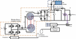
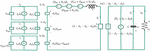
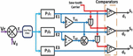
The proposed charging system architecture is shown in Figure 1. The main parts of the dual input charging system are wireless charger, solar PV array, controller, battery, and DIBBC. The diagram includes a solar PV array and a detailed circuit of wireless chargers. Three switches S, S, and S are connected between the source section and converter output through single inductor L, and diode D. Solar PV source consists of the solar panel and reverse protection diode D. Wireless charger system is powered by a DC source as in the proposed architecture or it can be powered from the grid through a rectifier and filter such as in a battery charging station. The power from the DC source is converter to high-frequency AC, i.e., 85kHz, through a high-frequency inverter. This high-frequency AC powers a primary or transmitter coil network consisting of an inductor L and compensation capacitor C, designed to achieve series resonance conditions at 85kHz frequency. Similarly, the same values of inductor and capacitor are used to design secondary or receiver side series resonant network for 85kHz frequency. Across the receiver side output terminals, rectifier is connected to which converters received AC power to DC. A constant output voltage is maintained at one input of the dual input dc-dc converter under no-load condition. Solar PV acts as the second input to the dual input converter. The working of the DIBBC is discussed in section 3 in detail.
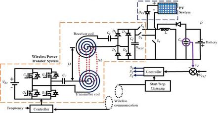
Figure 1 Proposed architecture for integrated WPT plus solar PV based EV charging.
2.1 On-board Solar PV System
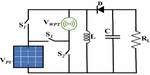
An accurate equivalent circuit of solar PV source is shown in Figure 2. In the proposed architecture, a solar panel needs to be placed on the rooftop of EV. This will allow regular cooling of the panel while driving and charging the battery. Under favorable weather conditions, the photocurrent generated by the panel is I and is computed by using (1). The Current supplied by PV panel to the dual input converter is given by (2). Solar PV current and voltage are denoted by I and V. Energy from solar irradiance(I) is converted to photocurrent, under temperature (T). The short circuit current (I) under 1000W/m is given by K and R, R is the internal shunt and series resistance of the PV panel. Thermal voltage (V) across the shunt diode(D) varies with temperature. Based on load requirement, the number of series (N) and parallel (N) connected solar PV modules can be selected to get the desired output voltage and current. The saturation current (I) of the solar PV panel and it varies with the number of photons and frequency of irradiance shown on the PV panel.
The open-circuit voltage (V) can be derived from (2) by substituting I 0 and short circuit current (I) by substituting V 0 [23]. Voltage and current supplied by the solar PV module to load is V and I. Discussion on solar PV system is restricted till basic working.
| (1) | ||
| (2) |
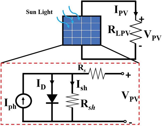
Figure 2 Solar PV equivalent circuit.
2.2 Wireless Charging System
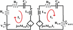
The equivalent circuit of the two-coil wireless charger portion of the proposed system is shown in Figure 3.
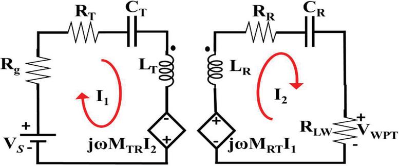
Figure 3 Two coil equivalent circuit.
In Figure 3, Vs and I are the primary source voltage and current. V is the receiver side voltage across the load R and current across the load on receiver side is I. R is the source resistance on the primary side. R and R are transmitter coil and receiver coil resistance. Compensating capacitor C and C are required to compensate the coil inductance L and L to obtain the resonance condition in WPT system. The mutual inductance of the two-coil system between the TxC and RxC is or is denoted by M.
‘R’ load resistance referred to the secondary side from rectifier output is given by
| (3) |
The reflected resistance (R) from the receiver side to the transmitter side is given by
| (4) |
The total resistance (R) of the two-coil circuit referred to the primary is given by
| (5) |
The relation is derived by taking the considerations of the resonance condition ie, inductive reactance (X X).
| (6) |
By applying KVL to the above circuit
| (7) | |
| (8) |
The primary coil and secondary coil currents are as given by
| (9) |
The input and output power of the two-coil system are given by
| (10) |
The simplified expression for the efficiency of the two-coil system is given by
| (11) |
In Equation (11), , , and are given by
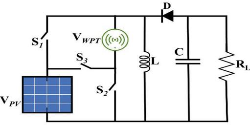
Figure 4 Dual input buck-boost dc-dc converter (DIBBC).
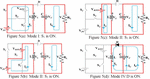
3 Modes of Operation
The circuit diagram of the DIBBC is shown in Figure 4. V and V represent the voltage values of the two sources and S, S and S are the three switches of the DIBBC. The remaining part of the DIBBC is similar in design to a conventional buck-boost converter with inductor (L), capacitor (C) and load resistance R. Working of the dual input converter is shown in diagrams Figure 5(a) to 5(d). Table 1. provides the details for state of switches, diodes and other elements and load in the circuit. Timing diagram in Figure 6 shows states of the gate pulses given to the switches along with voltage and current across the inductor.
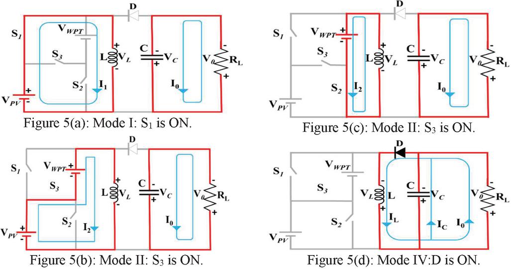
Figure 5
Table 1 Modes of operation
| Mode | S | S | S | D | V | I | V | I |
| I (t 0 to t dT) | ON | OFF | OFF | OFF | V | I | V | I |
| II (t dT to t dT) | OFF | OFF | ON | OFF | V+V | I | V | I |
| III (t dT to t dT) | OFF | ON | OFF | OFF | V | I | -V | I |
| IV (t dT to t T) | OFF | OFF | OFF | ON | V | I | V | I |
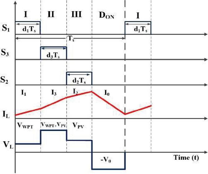
Figure 6 Timing diagram for continuous-conduction mode (CCM).
4 Small Signal Modelling of DIBBC
The state-space model of DIBBC can be expressed as given in (12) and (13).
| (12) | ||
| (13) |
Here A is the state matrix, B is the input matrix, C is the output matrix and D is the feed-forward matrix. Matrix , U, Y and [M] are as given below.
The small signal model of the DIBBC is derived and given by (14) and (15).
| (14) | ||
| (15) |
For obtaining the small signal model circuit expand the state Equation (14)
| (16) | |
| (17) |
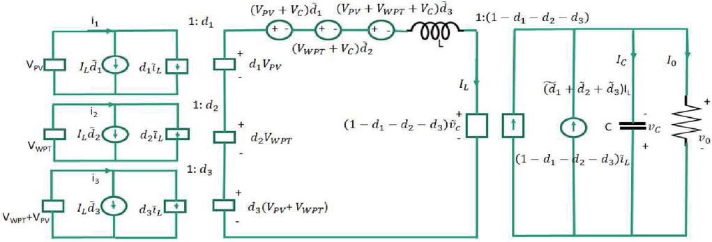
Figure 7 Small signal model circuit of DIBBC.
Also form output Equation (15)
| (18) |
By using the equations derived from the (14) and (15), the equivalent small-signal modal circuit is obtained for the three different duty ratios shown in the Figure 7.
The effect of small-signal test disturbance can be observed through analyzing the transfer functions derived from the small-signal model. The response of due to small signal test disturbance injected in the duty ratio can be measured based on the small signal model given in (14) and (15) by fixing the remaining input small signal test disturbance values and to zero. In similar fashion, the response of due to small signal test disturbances in, , and can be measured with the transfer functions given in (19), (20) and (21) below.
| (19) | ||
| (20) | ||
| (21) |
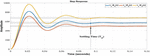
The three transfer functions (19), (20), and (21) are evaluated with the respective step response shown in Figure 8. The step response settles at their respective DC gain value of 507, 580.76, and 691.1. The peak overshoot of the three transfer functions varies as the input voltage for each transfer function is different. Solar PV and WPT source voltages are 60V and 36V. It can be seen, the peak overshoot response and steady-state value for the transfer function (21) are higher as the input voltage, and DC gain is higher compared to transfer function (19) and (20). Thus, peak overshoot magnitude and oscillations depend on the DC gain and input voltage. Settling time (T) for the three transfer functions is equal to 0.095 seconds as obtained from the step response. The pole-zero map and bode plot is shown in Figures 9 and 10, the system is stable as there are no open-loop poles on the RHS of the S-plane and the phase margin of the three transfer functions is positive, the details are given in Table 2. The eigenvalues of the characteristic equations are 0.3846 1.4109i and 0.3846 1.4109i. Also, as it is seen, the peak overshoot and DC gain of (21) are higher, so the stability limit, i.e., the phase margin is least for . A suitable controller is thus required to shift the phase margin of the transfer functions to greater than at least 40db.
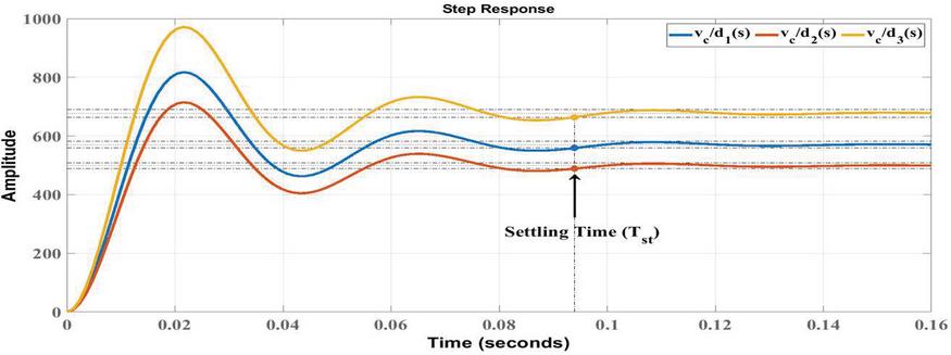
Figure 8 Step response of transfer functions.
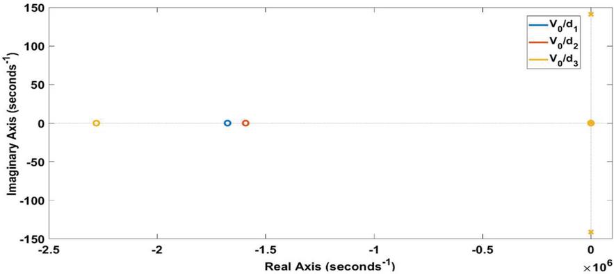
Figure 9 Pole-zero location of transfer function.
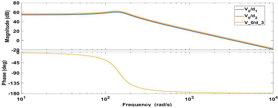
Figure 10 Bode plots of open loop transfer function.
Table 2 Open loop relative stability parameters
| Gain | Phase | |||
| DC | Margin | Margin | ||
| Transfer Function | Gain | (GM) | (PM) | Stability |
| 507 | Infinity | 1.47 | Stable | |
| 580.76 | Infinity | 1.37 | Stable | |
| 691.1 | Infinity | 1.25 | Stable |
5 Control Scheme For DIBBC
The controller for the DIBBC is modeled as shown in Figure 11. The error signal E is fed to three PI controllers. The value of K and K for each controller is modeled using the transfer function (19), (20), and (21). Switching time dT, dT, and dT for the switches S, S, and S is controlled by converting the output of PI controllers to time delay (T, T, and T) values for the respective switching time-period. This time delay value is used to delay the sawtooth reference carrier of the next switch to be turned ON. Switch S is set as the reference, i.e., sawtooth carrier for S is not delayed, and PI output is used to delay the S switch carrier. The addition of PI and PI is used to delay the carrier of S. The output of PIis not used to delay as there is not next switch for controlling. This scheme can be adopted for N input DC-DC converter as well.
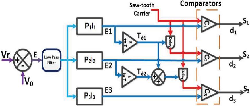
Figure 11 Control scheme for DIBBC.
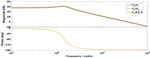
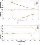
Bode plots for the compensated and uncompensated system is shown in Figure 12. The details of Gain Margin(GM) and Phase Margin(PM) of controller transfer function with gain cross over frequency (W) & phase cross over frequency (W) are given in Table 2.
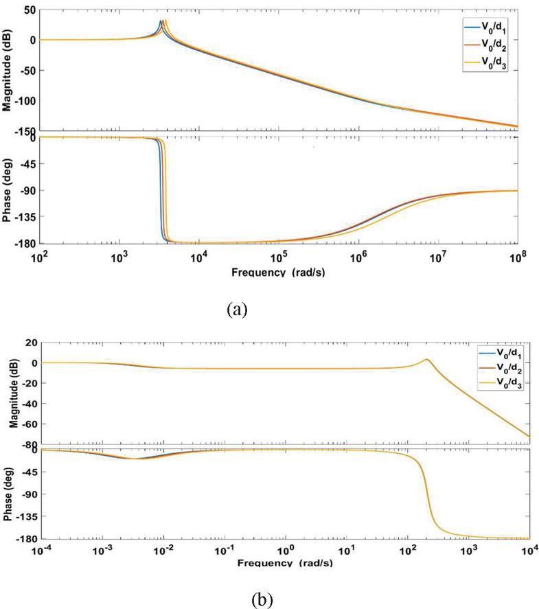
Figure 12 Closed-loop bode plots (a) without controller (b) with controller.
Table 3 Closed-loop stability analysis of DIBB converter
| Transfer | Controller | GM & PM | |||
| Function | K | K | Transfer Function | with Controller | W & W |
| 0.0029 | 0.0001 | 42, Infinity | Inf, 276.04 | ||
| 0.0027 | 0.0001 | 40.1, Infinity | Inf, 283.7 | ||
| 0.0022 | 0.0001 | 41.4, Infinity | Inf, 279.7 |
6 Results and Discussion
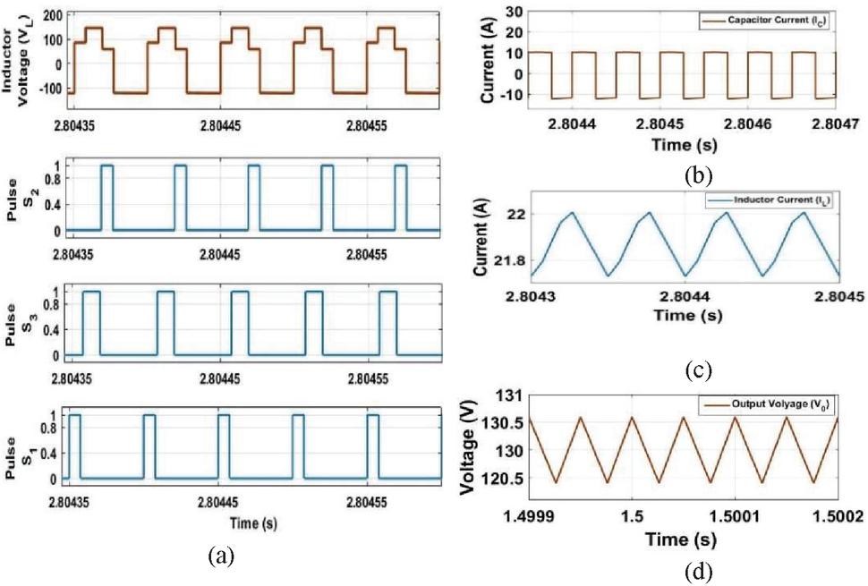
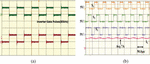
Figure 13 DIBBC behaviour (a) inductor voltage and switching pulses (b) inductor current (c) capacitor current (I) and (d) output voltage (V).
6.1 Simulation Results
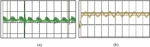
DIBBC design is simulated in MATLAB Simulink. PI Controller values designed with the help of transfer functions , , and are used in the designed control scheme explained in the previous section. The steady-state switching pulses and inductor voltage for the four modes of operation observed in the simulation are shown in Figure 13(a). The switching pattern of the switches matches well with the theoretical timing diagram. Inductor current and capacitor current ripples under steady-state are shown in Figure 13(b) and (c). In the rising portion of the inductor current (I) three slopes are observed, which indicate the initial three modes of operation during which the inductor is charged from the sources. Capacitor current (I) profile consists of charging and discharging current. The negative current is the discharging portion i.e., The first three modes of operation of the dual input converter. The positive portion is the charging operation during the fourth mode of operation of the converter. During the fourth mode, the inductor discharges across the capacitor along with the load to power up the capacitor for the next switching cycle. Output voltage ripple of 1V is observed in the voltage profile during the steady-state Figure 13(d). This is less than 1% of the output voltage. Thus, the inductor and capacitor values are well suitable for the simulated source voltages and desired output voltage of 130V and 10A load current.
Controller performance is evaluated by injecting a disturbance in the two DC sources. The output voltage and output current during the disturbance injection in the sources is shown in Figure 14(a) and (b). The initial state of the output voltage, output current is settled at 130V/10A. During disturbance injection in both sources, the output voltage and current deviate for a short time from the desired values. When both the sources have negative disturbance, the output voltage falls and vice versa. The effect on output voltage is minor if one input source suffers positive disturbance while the other suffers negative disturbance. In all the disturbances shown in Figure 14(a), the controller is robust enough to maintain the output voltage equal to the desired value within a short period after disturbance injection. During the disturbance, the inductor current reduces, increases when the sum of the voltage sources deviates in positive, negative from the normal condition (60V36V).
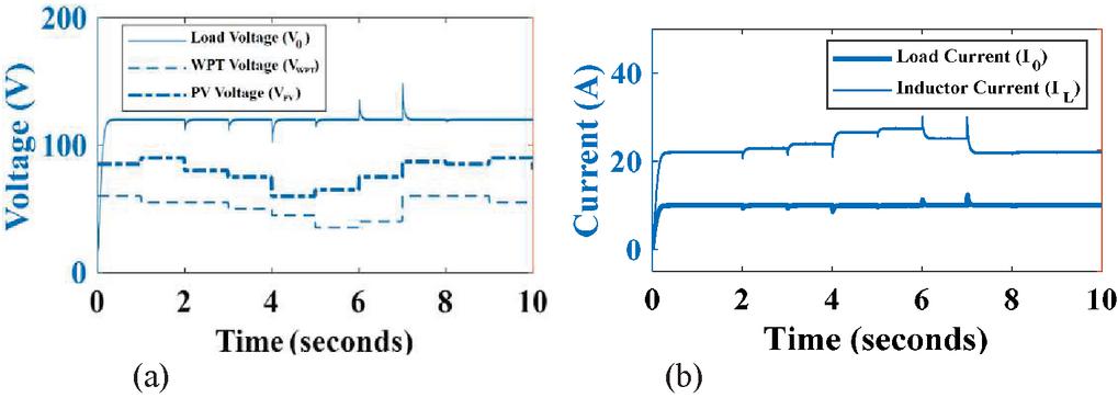
Figure 14 Effect of input source variations (a) system voltages (b) load current.
6.2 Hardware Results
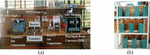
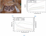
The hardware setup shown in Figure 15(a) is tested for desired output voltage of 130V with resistive load and a battery stack shown in Figure 15(b). Details of different specifications of the hardware setup are given in Tables 4–6. Solar PV is substituted by a solar simulator for hardware analysis and evaluating working of the proposed system. The high frequency inverter and DIBBC are independent controlled switching pulses by SPARTAN-6 FPGA board shown in Figure 16.

Figure 15 Hardware setup (a) integrated wireless plus solar PV based EV charging system test bench (b) battery stack.
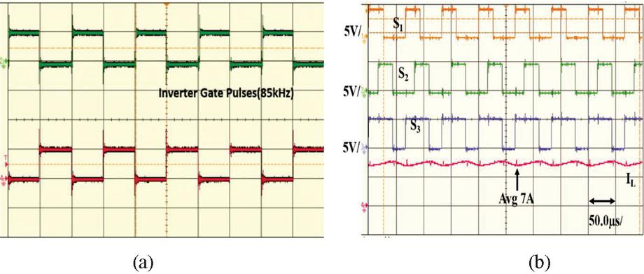
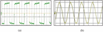
Figure 16 Gate pulses for (a) inverter switches (G1–G4) (b) DIBB converter switches (S1–S3).
Table 4 Wireless power transfer (WPT) system specifications
| Parameter | Transmitter Coil (TxC) | Receiver Coil (RxC) |
| Turns | 27 | 27 |
| Strands/SWG | 1500/42 | 1500/42 |
| Resonance Frequency | 85kHz | 85kHz |
| Self-inductance (H) | 112.2 | 112.2 |
| Compensating capacitor (nF) | 31.22 | 31.22 |
| Coil resistance () | 1.5 | 1.5 |
| Wire diameter (mm) | 5.5 | 5.5 |
| Inner radius (mm) | 25 | 25 |
| Outer radius(mm) | 175 | 175 |
| Shape | Circular | Circular |
Table 5 DIBBC simulation and hardware design comparison
| Parameter | Simulation Value | Hardware Value |
| Inductor | 6 mH | 5.5 mH |
| Filter Capacitor | 1000 F | 2000 F |
| Load | 12 | 0–50 |
| Battery | Lead Acid 120V/165 Ah | Lead-Acid 200 Ah 10Nos12V/20 Ah |
Table 6 Specification of solar PV in solar simulator
| Parameter | Value |
| No. of Series/Parallel | 2/3 |
| Open-circuit voltage (V) | 37.2V |
| Short circuit current (I) | 8.62A |
| Maximum power condition | 30.2V/8.1A |
| Maximum power (W) | 213.5W |
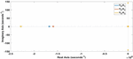
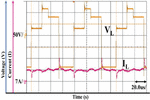
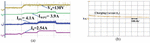
The coil arrangement for the WPT system is shown in Figure 17(a). Before connected to the DIBB converter, the WPT system is tested for the different distances to obtain the optimal distance; from this, 10cm distance is chosen because it has good average efficiency and also better output power. The power and efficiency plots for various distances between the transmitter and receiver are shown in Figure 17(b) and (c). Transmitter coil and Receiver coil input voltage and current are shown in Figures 18 and 19. Also, input to the dual input converter from the wireless charger source after rectification and filtering is shown in Figure 20. The ripples in the transmitter voltage are observed due to incomplete compensation of the reactive power drawn by the coils. The nature of transmitter current is observed to be peaky sinusoidal in one half due to the saturation from harmonic components as seen in transformers. Similarly, the receiver side voltage is not an exact square wave due to incomplete compensation coils. The load voltage shown in Figure.20 is measured across the filter capacitor connected across the WPT input terminals of the DIBBC. The rectifier output current passes a filter inductor and flows to the filter capacitor and input to the DIBBC.
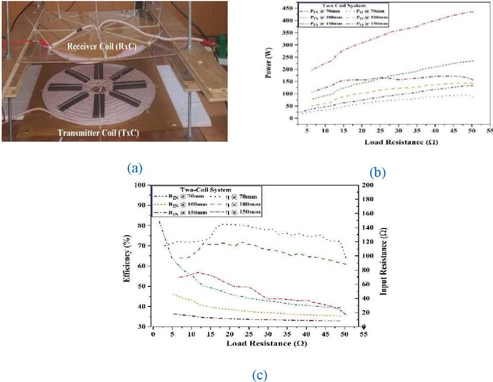
Figure 17 (a) Two coil system arrangement (b) Efficiency plots for the different transmission distance (c) Power plots for different transmission distance.
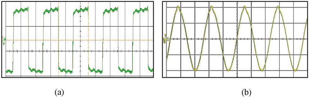
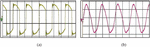
Figure 18 WPT system transmitter (a) voltage (150V) and (b) current (I=6.9A).
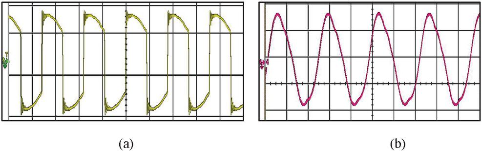
Figure 19 WPT system receiver (a) voltage (65V) and (b) Current (IA).
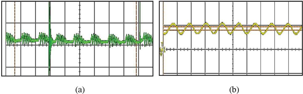
Figure 20 WPT system input to DIBBC (a) voltage (60V) and (b) current (Irms 4.6A).
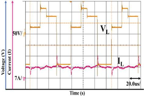
Figure 21 Integrated charging system inductor voltage (V) and inductor current (I).
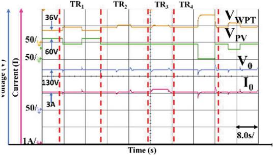
Figure 22 Charging system response under variable source operation.
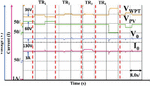
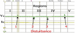
The two sources WPT and solar PV or solar simulator, are maintained at 36V and 60V. The system is tested by inducing disturbance by varying source voltages of the DIBBC. The DIBBC is tested for four test conditions, i.e. V varying, V varying, R varying and solar PV off. Inductor voltage (V) and inductor current (I) for the converter is shown in Figure 21. The test regions in Figure 22 show that the variations in solar PV and load side vary the output from the WPT source. When the load is increased i.e., test region 3, the solar PV output voltage is constant whereas, the WPT voltage increases details are tabulated in Table 7. Also, the WPT source is successful in. maintaining the demand by the load in the absence of solar PV. In Figure 23 DIBBC is operated as a single source DC-DC converter, and output is constant in both cases.
Table 7 Test Regions for Experimental Analysis of DIBBC
| Test Region | Load | V | V | V | I |
| TR | Constant | Decreased | Increases | Constant | Constant |
| TR | Constant | Constant | Decreased | Constant | Constant |
| TR | Increased | Constant | Increases | Constant | Increases |
| TR | Constant | OFF | Increases | Constant | Constant |
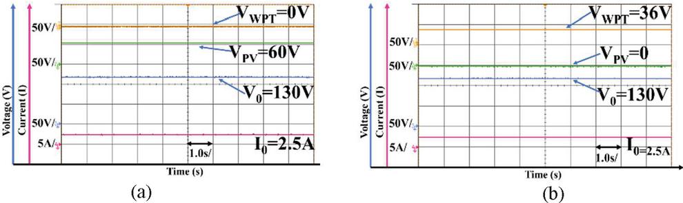
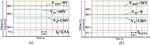
Figure 23 Single source operation of DIBBC (a) only solar PV active (b) Only WPT active.
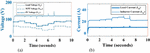
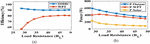
Current drawn by DIBBC when operated with WPT source is 12.5A at 36V and 3A at 109.4V. The efficiency of the dual input converter is 87.3% when only WPT input is active and 72.2% when the only solar simulator is active. Thus, the efficiency of the DIBBC is high for high source voltages as seen with WPT source. To improve the efficiency with solar PV, high voltage solar PV module should be used. During dual source operation for output voltage of 130V when input sources are set to 36V and 60V, the currents supplied by both sources are 3.9A from WPT source and 4.1A from solar simulator source. WPT source current (I), solar PV current (I), load current and load voltage profile during the variation of load from 50 to 28 are shown in Figure 24(a). During the dual-source operation, the load is varying from 28 to 50 and the efficiency plot for the same is given in Figure 25(a) and power plot in Figure 25(b). Also, the battery charging current is shown in Figure 24(b) is recorded for 120V/200Ah battery stack. The charging current during constant voltage charging decreases from 4A to 1.5A in the charging duration of 1000 seconds.
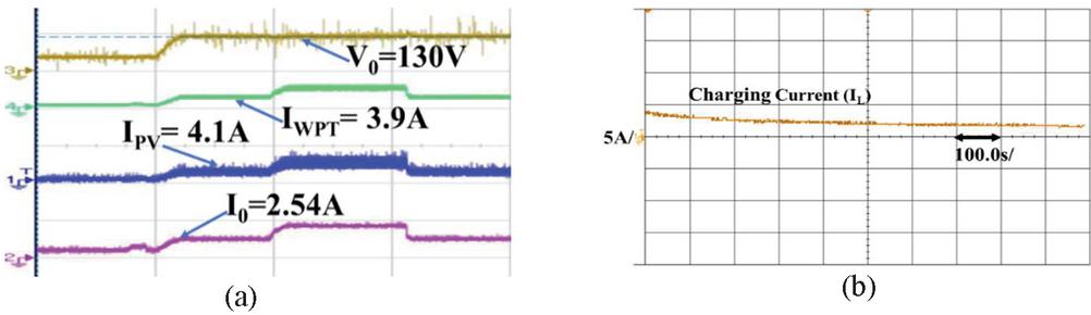
Figure 24 (a) DIBBC system load voltage and current profiles for varying load conditions. (b) charging current under constant voltage charging mode.
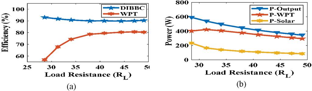
Figure 25 Charging system performance (a) efficiency of WPT and DIBBC (b) power output of DIBBC, input power from WPT and solar PV source.

Figure 26 Loss distribution of (a) dual input buck-boost converter and (b) wireless power transfer system.
The efficiency of the converter and WPT system is measured for different load values are shown in Figure 25(a). The majority of the power to the load is supplied from WPT system. Change in load resistance causes power flow from both the source to change while keeping the percentage of power supplied by the two sources to be unaltered. Also, it can be seen from the efficiency and power plots; the converter is more efficient when the difference between the power supplied from the two sources is least. This is observed at 28 load and also at 50 load. Thus, if both the sources supply equal power, the converter can perform more efficiently and can maintain high-efficiency values for different loads as well. The average loss distribution pie chart for the dual input converter and WPT system is shown in Figure 26. Losses in switches of DIBB converter are the switching losses, off-state leakage losses, and conduction losses. S contributes the majority of the switch losses as it operates when both the sources are connected in series. Thus, the current slope is higher when compared to the S and S. S connects WPT source to the solar PV to the inductor, and as a result of the higher source voltage, the losses are higher for S compared to S. Thus, the source voltage is observed to be the main parameter for causing losses. The major component in the dual input converter is the inductor mainly due to its significant internal resistance of around 0.3 . Although in the pie chart, the inductor and capacitor are summed to a single section, the major loss contribution is by the inductor. Diode D conducts for only T(1–d–d–d) units of the switching cycle, which is very low and thus the loss occurring in the diode D are low. The switch losses are a sum of conduction, switching, OFF-state leakage current, and collector to emitter resistance drop. In WPT system the TxC, RxC and inverter are the major loss contributing components. The highest loss occurs in the receiver coil mainly due to harmonics and compensation. Thus, a detailed study to improve the coil fabrication and compensation topology is required to improve the efficiency of the WPT system. Also, the implementation of an effective PWM generation algorithm to reduce the harmonics will greatly contribute to further increase the efficiency of the WPT system. Similarly, designing a dual input converter control algorithm to reduce the losses and manage the power flow efficiently will significantly improve and maintain the efficiency of the converter for varying loads and source voltages.
The solar simulator voltage is varied to simulate solar irradiance changes and the output voltage of the converter is recorded for the same disturbances and are shown in Figure 27. It can be observed the converter output voltage settles quickly to the set reference with a maximum peak overshoot of 5V to 7V given in Table 8. Thus, the controller is effective in canceling the effect of source disturbance on the output voltage.
Table 8 Variations in the solar irradiation
| Disturbance Positions | 1 | 2 | 3 | 4 |
| Solar Simulator Voltage (V) | 70 | 60 | 50 | 60 |
| Settling time (t) | 2.06 | 4.2 | 2.6 | 2.6 |
| Peak Overshoot (M) | 7 | 8.25 | 8.25 | 8.5 |
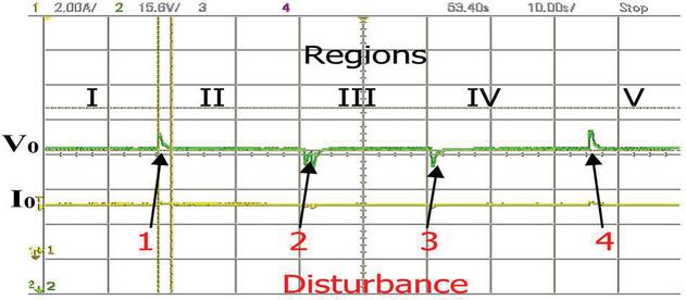
Figure 27 Disturbance analysis for Solar PV voltage (V) variation.
A comparison of the proposed system with state-of-the-art literature is produced in Table 9. The comparison highlights no of components in the converter, the number of converter operations possible, and the type of dual input integration tested. Thus, the integration of WPT and On-board Solar PV studied in this paper is tested with the dual input converter topology.
Table 9 Comparison of the existing works with the proposed work
| Parameter | [15] | [16] | [18] | [22] | Proposed |
| No of IGBT | 3 | 4 | 4 | 6 | 3 |
| No of Diode | 1 | 6 | 2 | 6 | 1 |
| L | 1 | 1 | 1 | 1 | 1 |
| C | 1 | 1 | 1 | 1 | 1 |
| Modes | 1 | 1 | 3 | 3 | 1 |
| Bidirectional | No | Yes | Yes | Yes | No |
| Efficiency | 88%–90% | 84%–94% | 80%–94% | 82%–91% | 85%–92% |
7 Conclusion
This paper study investigates the performance of a dual input buck-boost converter (DIBBC) for renewable source integration with wireless charger for EVs to reduce stress on the grid. On-board solar PV is the renewable energy source, and WPT system is the wireless charger. Small signal model of the DIBBC is derived and further transfer function for each switch S, S and S is derived. PI controller for each switch is designed using the transfer function of the respective switch and a control scheme is developed to operate the three switches to maintain the output voltage constant of the DIBBC during any disturbance. The simulation studies of the DIBBC are done in MATLAB Simulink. Simulation results show robust performance by the controller during disturbance injection in the two input sources.
Hardware analysis of the DIBBC is done with a wireless charging system and solar simulator. The solar simulator is programmed to operate as 60V/25A solar PV module. Efficiency of the DIBBC was observed to be always above 85% for the load range 28 to 50 for an output voltage of 130V. Detailed investigation of losses in the converter has also been discussed. Single source operation of the dual input converter gives low efficiency with WPT system as it supplies power at low voltage. Also, when the two sources are supplying almost equal power the converter performance is further improved. The controller implemented for the developed DIBBC does not include MPPT feature and thus the efficiency with actual solar PV panel can be less. Integrating MPPT control technique with the proposed control scheme can improve the efficiency of the DIBBC as well as the solar PV performance. Further works on the proposed system can be the bidirectional operation of the converter for V2G using wireless power transfer and integration of MPPT in the control scheme.
Acknowledgement
The authors are thankful to CPRI Bangalore (RSOP/2019/GD/10), Ministry of Power, Govt. of India for providing funding support for this research.
References
[1] Vithayasrichareon, Peerapat, Graham Mills, and Iain F.MacGill. “Impact of electric vehicles and solar PV on future generation portfolio investment.” IEEE Transactions on sustainable energy 6, no. 3 (2015): 899–908.
[2] Shariff, Samir M., Mohammad Saad Alam, Furkan Ahmad, Yasser Rafat, M. Syed Jamil Asghar, and Saadullah Khan. “System design and realization of a solar-powered electric vehicle charging station.” IEEE Systems Journal 14, no. 2 (2019): 2748–2758.
[3] Kabir, Mohammad Ekramul, Chadi Assi, Mosaddek Hossain Kamal Tushar, and Jun Yan. “Optimal scheduling of ev charging at a solar power-based charging station.” IEEE Systems Journal 14, no. 3 (2020): 4221–4231.
[4] Tran, Viet Thang, Md Rabiul Islam, Kashem M. Muttaqi, and Danny Sutanto. “An efficient energy management approach for a solar-powered EV battery charging facility to support distribution grids.” IEEE Transactions on Industry Applications 55, no. 6 (2019): 6517–6526.
[5] Schuss, Christian, Tapio Fabritius, Bernd Eichberger, and Timo Rahkonen. “Impacts on the Output Power of Photovoltaics on Top of Electric and Hybrid Electric Vehicles.” IEEE Transactions on Instrumentation and Measurement 69, no. 5 (2019): 2449–2458.
[6] Subudhi, Partha Sarathi, Krithiga Subramanian, and Binu Ben Jose Dharmaian Retnam. “Wireless electric vehicle battery-charging system for solar-powered residential applications.” International Journal of Power and Energy Systems 39, no. 3 (2019).
[7] Mallon, Kevin R., Francis Assadian, and Bo Fu. “Analysis of on-board photovoltaics for a battery electric bus and their impact on battery lifespan.” Energies 10, no. 7 (2017): 943.
[8] Hu, Yihua, Chun Gan, Wenping Cao, Youtong Fang, Stephen J. Finney, and Jianhua Wu. “Solar PV-powered SRM drive for EVs with flexible energy control functions.” IEEE Transactions on Industry Applications 52, no. 4 (2016): 3357–3366.
[9] De Pinto, Stefano, Qian Lu, Pablo Camocardi, Christoforos Chatzikomis, Aldo Sorniotti, Domenico Ragonese, Gregorio Iuzzolino, Pietro Perlo, and Constantina Lekakou. “Electric vehicle driving range extension using photovoltaic panels.” In 2016 IEEE Vehicle Power and Propulsion Conference (VPPC), pp. 1–6. IEEE, 2016.
[10] Shuo, W. A. N. G., and D. G. Dorrell. “Loss analysis of circular wireless EV charging coupler.” IEEE Transactions on Magnetics Mag 50, no. 11 (2014): 1–4.
[11] Rozman, Matjaz, Augustine Ikpehai, Bamidele Adebisi, Khaled M. Rabie, Haris Gacanin, Helen Ji, and Michael Fernando. “Smart wireless power transmission system for autonomous EV charging.” IEEE Access 7 (2019): 112240–112248.
[12] S. Chopra and P. Bauer, “Driving Range Extension of EV With On-Road Contactless Power Transfer—A Case Study,” in IEEE Transactions on Industrial Electronics, vol. 60, no. 1, pp. 329–338, Jan. 2013, doi: 10.1109/TIE.2011.2182015.
[13] Subudhi, Partha Sarathi and S, Krithiga. “Wireless Power Transfer Topologies used for Static and Dynamic Charging of EV Battery: A Review,” International Journal of Emerging Electric Power Systems, vol. 21, no. 1, 2020, pp. 20190151. https://doi.org/10.1515/ijeeps-2019-0151.
[14] Kalialakis C., Collado A., Georgiadis A. (2016) Regulations and Standards for Wireless Power Transfer Systems. In: Nikoletseas S., Yang Y., Georgiadis A. (eds) Wireless Power Transfer Algorithms, Technologies and Applications in Ad Hoc Communication Networks. Springer, Cham. https://doi.org/10.1007/978-3-319-46810-5_7.
[15] Athikkal, Sivaprasad, Gangavarapu Guru Kumar, Kumaravel Sundaramoorthy, and Ashok Sankar. “Performance analysis of novel bridge type dual input DC-DC converters.” IEEE Access 5 (2017): 15340–15353.
[16] Athikkal, Sivaprasad, Gangavarapu Guru Kumar, Kumaravel Sundaramoorthy, and Ashok Sankar. “A non-isolated bridge-type DC–DC converter for hybrid energy source integration.” IEEE Transactions on Industry Applications 55, no. 4 (2019): 4033–4043.
[17] Athikkal, Sivaprasad, Kumaravel Sundaramoorthy, and Ashok Sankar. “Design, Fabrication and Performance Analysis of a Two Input—Single Output DC-DC Converter.” Energies 10, no. 9 (2017): 1410.
[18] Kumaravel, S., G. Guru Kumar, Kuruva Veeranna, and V. Karthikeyan. “Novel Non-isolated Modified Interleaved DC-DC Converter to Integrate Ultracapacitor and Battery Sources for Electric Vehicle Application.” In 2018 20th National Power Systems Conference (NPSC), pp. 1–6. IEEE, 2018.
[19] Singh, Ankit Kumar, Manoj Badoni, and Yogesh N. Tatte. “A Multifunctional Solar PV and Grid Based On-Board Converter for Electric Vehicles.” IEEE Transactions on Vehicular Technology 69, no. 4 (2020): 3717–3727.
[20] D. K. Behera, I. Anand, B. Malakonda Reddy and S. Senthilkumar, “A Novel Control Scheme for a Standalone Solar PV System Employing a Multiport DC-DC Converter,” 2018 9th International Conference on Computing, Communication and Networking Technologies (ICCCNT), Bengaluru, India, 2018, pp. 1–6, doi: 10.1109/ICCCNT.2018.8494101.
[21] P. S. R. Nayak, K. Kamalapathi, N. Laxman and V. K. Tyagi, “Design and Simulation Of BUCK-BOOST Type Dual Input DC-DC Converter for Battery Charging Application in Electric Vehicle,” 2021 International Conference on Sustainable Energy and Future Electric Transportation (SEFET), Hyderabad, India, 2021, pp. 1–6, doi: 10.1109/SeFet48154.2021.9375658.
[22] Kumar, Lalit, and Shailendra Jain. “Multiple-input DC/DC converter topology for hybrid energy system.” IET Power Electronics 6, no. 8 (2013): 1483–1501.
[23] Nguyen, X.H., Nguyen, M.P. Mathematical modeling of photovoltaic cell/module/arrays with tags in Matlab/Simulink. Environ Syst Res 4, 24 (2015).
Biographies

Kuditi Kamalapathi received the B.Tech. degree in electrical and electronics engineering from JNTU Hyderabad, Telangana, India, in 2008; and the M.Tech. degree in Power Electronics and Drives, from VIT University, Vellore, Tamilnadu, India, in 2010. From 2010–2017 worked as an assistant professor at SV College of Engineering, Tirupati. Currently, he is pursuing a Ph.D. degree in electrical and electronics engineering from the National Institute of Technology, Tiruchirappalli, Tamil Nadu, India. His research interests include power electronics and wireless power transfer systems.

Panugothu Srinivasan Rao Nayak was born in Perikapadu, Guntur, Andhra Pradesh, India, in 1979. He received the B.Tech. degree in electrical and electronics engineering from Bapatla Engineering College (BEC), Bapatla, Guntur, in 2001; the M.Tech. degree in energy systems from Jawaharlal Nehru Technological University (JNTU), Hyderabad, Telangana, India, in 2006; and the Ph.D. degree in electrical engineering from the National Institute of Technology, Tiruchirappalli, Tamil Nadu, India, in 2014. Currently, he is an Assistant Professor with the Department of Electrical and Electronics Engineering, National Institute of Technology. His research interests include power electronics and drives, biologically inspired optimization techniques and wireless power transfer systems.

Vipul Kumar Tyagi received B. Tech degree in electrical and electronics engineering from Bhagwant University, Ajmer, Rajasthan, India, 2016 and M.Tech degree in Power & Energy, from Amrita Vishwa Vidhyapeetham, Amritapuri, Kerala, India, 2019. Currently, he is working as Junior Research Fellow in NIT Tiruchirappalli, Trichy, Tamil Nadu, India under CPRI sponsored project. His research interests include Wireless EV Charging, Smart Charging, Smart Metering and Demand Side Management for Load Congestion Mitigation.
Distributed Generation & Alternative Energy Journal, Vol. 37_1, 73–102.
doi: 10.13052/dgaej2156-3306.3714
© 2021 River Publishers