Low Frequency Operation and dsPIC Micro-controller Implementation for Multilevel Quasi Z Source Inverter in Photovoltaic Application
Salman Ahmad1,*, Rahim Uddin1, Zahoor Ahmad Ganie1, Ahmed Sharique Anees1 and Farhad Ilahi Bakhsh2
1Department of Electrical Engineering, Islamic University of Science and Technology, Kashmir, India
2Department of Electrical Engineering, National Institute of Technology, Srinagar, India
E-mail: salmanahmad19@gmail.com; alirahim2007@gmail.com; zahoor.ganie@islamicuniversity.edu.in; shariq.anees@gmail.com; farhad@nitsri.ac.in
*Corresponding Author
Received 27 August 2021; Accepted 15 November 2021; Publication 22 April 2022
Abstract
In this paper implementation of a micro-controller based pulse width modulation for multilevel quasi Z source inverter (qZSI) is presented. First implementation of component design of qZSI is taken into consideration with continuous and discontinuous operation mode. In this paper operation of multilevel qZSI with low switching frequency is presented. After this detailed modelling for qZSI is established for implementing of PIC microcontroller (PIC 16F877A) to generate the switching signals. Development ofa five-level quasi z-source inverter prototype is done and by proper adjustment of the shoot through (ST) switching state and non-shoot through (NST) switching state the control signal to the gate drivers is applied. Effective implementation of the proposed scheme is shown by the hardware result.
Keywords: Quasi-z source inverter, PIC microcontroller, pulse width modulation, multilevel inverter, solar photovoltaic, shoot through (ST) state.
Abbreviations
| qZSI | Quasi Z Source Inverter | VSI | Voltage Source Inverter |
| ZSI | Z Source Inverter | MPPT | Maximum Power Point Tracking |
| PV | Photovoltaic | CCM | Continous Conduction Mode |
| CHBMLI | Cascaded H-Bridge Multi Level Inverter | DCM | Discontinous Conduction Mode |
| DCMLI | Diode Clamp Multi Level Inverter | PWM | Pulse Width Modulation |
| THD | Total Harmonics Distortion | Voc | Open Circuit Voltage |
| NPC | Neutral Point Clamped | Isc | Short Circuit Current |
| PD | Phase Disposition | I | Cell Reverse Saturation Current |
1 Introduction
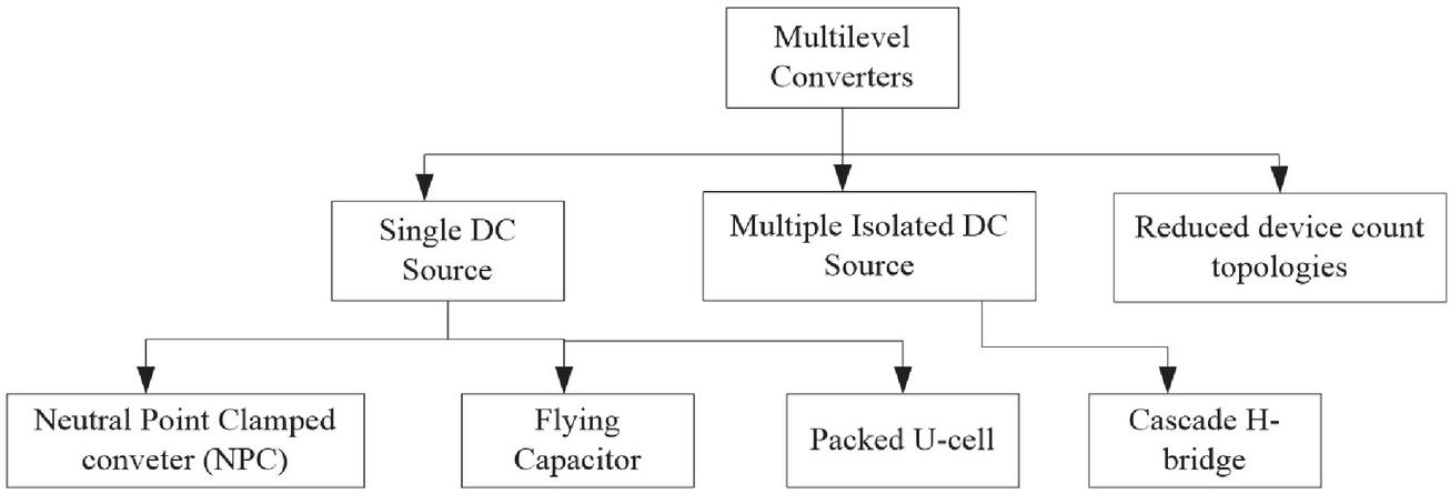
With the increasing dependence on photovoltaic (PV) system in grid connection mode, there is a sharp rise in the advancement of multilevel inverter applications. To process high power at medium voltage another choice is to have multilevel configuration [1]. It utilizes semiconductor devices of lower voltage and current ratings [2]. The multilevel inverter (MLI) topologies have various advantages than two-level configurations. The main advantage includes producing higher output voltages with limited switching device rating, lower dv/dt so lower the EMI, lower switching losses, lower total harmonics distortions and better efficiency [3]. A detailed classification of multilevel topologies is given in Figure 1 [4]. The commonly used Multilevel inverter topologies include active neutral point clamped inverter (ANPC), modular multilevel converters (MMC), packed E cell, packed U cell, flying capacitor (FC), neutral point clamped inverter (NPC) and cascaded H-bridge multilevel inverter (CHB) [2]. Several new topologies also have been presented in recent years [5]. The promising topologies are Cascaded Half-Bridge based Multilevel DC Link (MLDCL) Inverter, series connected switched sources (SCSS) based MLI, switched series/parallel sources (SSPS) based MLI, T-type inverter, cascaded bipolar switched cells (CBSC) based MLI, multilevel module (MLM) based MLI, two-switch enabled level-generation (2SELG) based MLI, reversing voltage (RV) topology and packed E-cell topologies. These topologies are created while considering the low switching device counts, maximum possible number of levels, application oriented etc [6]. Midst the numerous multilevel inverter topologies, the diode clamped multilevel inverter (DCMI) and cascaded H-bridge multilevel inverter (CHB) are the most common configurations which have been an area of active research. For high voltage output, the CHB and DCMI require a large number of modules, more switches, and more number of gate drivers and thus leading to increased cost and complexity [7, 8]. To overcome this limitation, the quasi Z-source (QZS) inverter and high gain Z-source inverter are gaining importance in the multilevel inverter configuration, where dc-link voltages have been boosted with the help of an LC-based network. The DC link of conventional VSI is replaced by Z source impedance network in a Quasi Z-source inverter and Z-source inverter which not only provides an additional stage of DC-DC boost to output voltage but also creates a new switching state i.e. shoot-through states [9, 10]. These inverters also provide protective enhancement of the switches without affecting the overall cost and efficiency. Areas such as solar photovoltaic, fuel cell stack, and batteries which require high voltage gain, extract the advantage of ZSI/QZSI. Multilevel ZSI/QZSI are best suited for high power and high voltage demand as there is increase in the number of inverter voltage, output ac waveform have low distortion with reduced blocking voltage across each switch. New PWM techniques based on phase disposition (PD) have been developed for multilevel configurations of ZSI/QZSI to have the gain through ST state. In [9, 10], the PD scheme for three levels NPC-ZSI which infers the boosted output voltage with less number commuted switch count have been discussed. Similarly [11, 12] analyze three-level NPC- QZSI which provide continuous dc source current along with a good boost factor.
Figure 1 Multilevel inverter classification.
QZSI, in continuous input current mode, is one of the improved topologies of basic ZSI. Based on continuity QZSI can be classified into Discontinuous QZSI (D-QZSI) & Continuous QZSI(C-QZSI). In D-QZSI, the common mode noise is less as both input source & DC-link has same earthing along with this the component rating is less compared with basic ZSI. C-QZSI possesses all the above merits of D-QZSI in addition it has continuous input current [13, 14]. On the basis of power flow, QZSI can be classified in unidirectional & bidirectional. Inherently QZSI is unidirectional but by replacement of the source diode with a bidirectional switch bidirectional QZSI is designed [15]. Recent literature mostly classifies QZSI based on boosting capacity of output power & dependence of voltage gain on modulation index. Switched inductor QZSI (SL-QZSI), switched Capacitor QZSI (SC-QZSI) and improved switched inductor QZSI (ISL-QZSI) are some of these new topologies. Figure 2 shows switched inductor cell, improved switched inductor cell and switched ccapacitor cell. The inductor on the inverter bridge side is replaced by these cells to form SL-QZSI, ISL-QZSI&SC-QZSI respectively [16–18].
Figure 2 (a) Switched inductor cell (b) improved switched inductor cell (c) switched capacitor cell.
Tapped Inductor Topology (TL-QZSI) proposed in [19] comments on the dependence of voltage gain on turn ratio. In cascaded QZSI/Extended boost QZSI, voltage gain is increased without increasing the number of active switches. High frequency Transformer Isolated QZSI (HFTI-QZSI) is proposed in [20, 21] inherits all the merits of QZSI and having electrical isolation between load & source. Detailed topological construction along with comparative assessment of various qZSI’s in photovoltaic application is given in [22]. A 9-level inverter design combining hybrid three-level modified-QZSI and a single-phase modified-QZSI is investigated in [20]. A significant boost of almost three times of dc link voltage of each cell and THD level of approximately 3% have been reported from the simulation & experimental results. A new five level QZS-NPC inverter is proposed in [21] having a level shifted carrier wave. The simulated results infer high boosted output voltage and good reactive power capability but it’s not validated experimentally. A two stage control method is presented in [22] for QZSI to control the output voltage & current. It also concludes that capacitor voltage controller for ZSI/QZSI is preferred above dc link controller for conventional VSI to boost output voltage. An inverted phase-shifted PWM scheme is employed for a five-level grid-connected QZSI injecting power into the PV-grid at reduced THD level is worked in [23]. The power is controlled using dc-link controller & independent MPPT control. The low switching frequency helps in reducing the switching losses considerably and hence is suited for voltage high power applications [24, 25]. The applications of qZSI have been worked out in various literatures considering the improvements in various parameters in [26–32]. Low switching frequency PWM techniques are useful in operation of voltage source converter as it will reduce the switching losses associated with the turning on and turning off of the semiconductor switches. It improves the overall system reliability. The main low switching frequency techniques available in the literature includes selective harmonics elimination (SHE) [33–41], selective harmonics mitigation (SHM) [42], pulse width amplitude modulation (PWAM) [43], nearest level control (NLC) [44], synchronous optimum pulse width modulation (SOPWM) etc. [45]. The SHE PWM technique has been widely investigated and used in various applications comparison to other low switching frequency techniques [40, 41].
In the manuscript, a quasi Z source based multilevel inverter configuration with a low switching frequency for solar photovoltaic operation is presented. The proposed technique decreases the switching losses and henceforth results in better reliability and efficiency of the power converters switches. The proposed model have been implemented using the dspic based microcontroller (PIC 16F877A), which is a low cost controller and thus results in cost effective solution. The dynamics modeling alongwith component design in continuous and discontinuous mode of operation for quasi network is provided for effective closed loop operation of the proposed low switching frequency technique. The five level qZSI prototype by having two H-bridge modules have been developed in the laboratory and PWM signals are applied by suitable adjustment of the shoot through switching states and non-shoot through switching states. The computational and hardware result display the effective implementation of the presented scheme. The PWM signals have been shown in separate figures to clearly identify the shoot through state and non-shoot through state of each power electronics switches and to indicate the switching frequency of the qZSI. The paper is divided as follows: Section 2 demonstrates the mathematical modeling of the solar photovoltaic system and qZSI alongwith CCM and DCM operation components design. Simulation and hardware results are obtained in Section 3. At the end Section 4 concludes the work done.
2 Mathematical Modelling
2.1 Solar Cell
Solar panels are constructed with solar cells as a basic component. Several solar cells are arranged in series and parallel combination to get desired voltage and currents at the output. The single solar cell diode model is the combination of a diode, two resistors, and a current source. To obtain the I-V, characteristics, the required expression can be derived and can be expressed by (1). From the expression, it is clear that the photocurrent is dependent on the solar irradiance and temperature of cell and therefore, it can be represented by (2).
| (1) | ||
| (2) |
Here I is at 25C short circuit current, T is the temperature of cell and k is the temperature coefficient of short circuit current. Diode current or the cell saturation current depends on cell temperature and is given by (3), I is the cell’s reverse saturation current at reference solar radiation and temperature and E represents the band gap energy of semiconductor utilized for manufacturing the cell. Also, the reverse saturation current is the current through the shunt resistor. The expression for the shunt current and the load current can be given by (4)–(5).
| (3) | ||
| (4) | ||
| (5) |
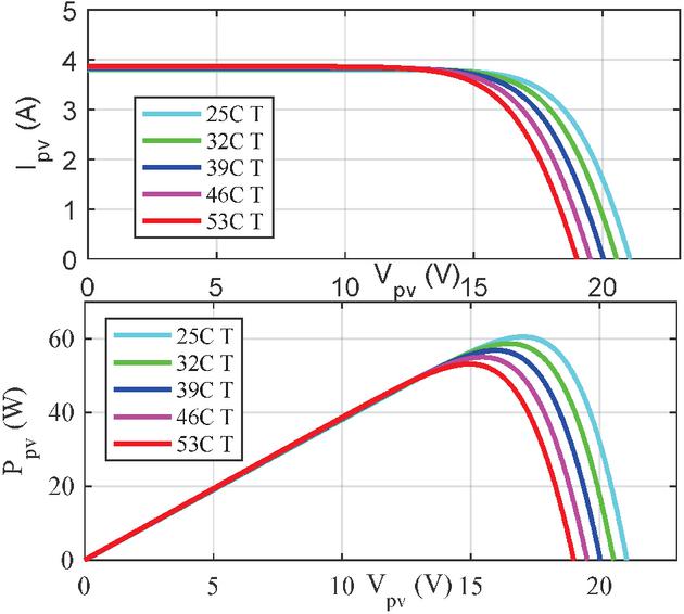
Where I is the generated current or photo current, I is the current saturation and R is resistance in series. Based on the mathematical modelling of single diode photovoltaic cell, the simulation model of PV cell is developed and the I-V, PV characteristics have been shown in Figure 3 for various values of Irradiance and temperatures.
2.2 Quasi Z Source Inverter
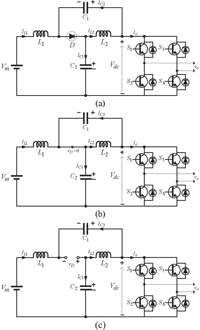
Buck or boost voltage operation for a single stage control is achieved in quasi Z-source inverter. In qZSI topology the controlled semiconductor switches can be simultaneously turned ON in the same leg and thus provides the gain in the output voltage. Also, it will remove the requirement of the dead time in practical implementation of the converter and therefore offers simplifications in control design. The single cell of the qZSI topology is given in Figure 4(a). For the construction of quasi network, two inductors and two capacitors are required. The shoot through (same switches in the leg are turned on), null and non-shoot through states or active states will charge or discharge these components based on the gain required in the output voltage. In the null state, simultaneous turning off of all the switches causes no power transfer from the input to the output side takes place. The equivalent circuit [46] of the qZSI in the non-shoot-through state and in the shoot-through state are shown in Figures 4(b) and 4(c), respectively.
Figure 3 TRINA solar TSM-250PA05.08 characteristics.
Figure 4 qZSI (a) circuit (b) equivalent circuit NST state(c) equivalent circuit ST state.
All the currents and the voltages are well-defined in the given figures and arrows represent the polarities. T is the time of one switching cycle, is the shoot-through state time interval, , the non-shoot-through state time interval, hence , and is the shoot-through duty ratio.
Thus, for the non-shoot-through (NST) state time interval , we get (6) and (7).
| (6) | ||
| (7) |
For the shoot-through (ST) state time interval , one can get (8)
| (8) |
The inductors average voltage at steady state over one switching cycle is zero. Therefore, we get (9) and on solving we can have (10).
| (9) |
Thus,
| (10) |
The inverter bridge’s peak dc-link voltage is,
| (11) |
Here, B is the qZSI boost factor. This is also the diode peak voltage. The inductor average current is calculated from the power rating P of the system
| (12) |
As per Kirchhoff’s current law and from the above equation (13), we can also get that
| (13) |
The current and voltage stress of the ZSI and qZSI are compared and have been shown in given in Table 1.
Table 1 Current and voltage stress in ZSI and qZSI
| ZSI | 0 | 0 | ||||
| qZSI | 0 | 0 | ||||
| ZSI | ||||||
| qZSI | ||||||
| ZSI | ||||||
| qZSI | ||||||
Here, m is the modulation index, P is the power rating of system and is the ac peak phase voltage. The relationships between modulation index and boost factor is given in (14).
| (14) |
From Table 1 it is clear qZSI has all advantages of ZSI. By a given boost factor it is possible to buck or boost voltage. ZSI can handle a shoot-through state, and thus has reliability greater than the traditional VSI. As compared to qZSI, ZSI has some exceptional merits i.e., ZSI sustains the same high voltage because of the presence of two capacitors while the voltage on capacitor in qZSI is lower, which means capacitor rating is lower. Also in the boost mode of ZSI, input current is discontinuous while there is continuous input current in qZSI due to the input inductor , which will minimise input stress. Also, there are less EMI problems.
2.3 CCM and DCM Analysis of qZSI
The performance of qZSI is affected by CCM and DCM conduction mode as the circuitry of qZSI internally has a DC-DC voltage boost structure with capacitors and inductors present intrinsically. The governing equations of qZSI are valid only in continuous conduction mode. However for DCM we need to formulate the new governing equations [47]. To yield the desirable results, the CCM and DCM operations are used to design the qZSI. The input inductor in the qZSI varies the source current of the qZSI network. Thus when during ST state the input current never drops to zero, the qZSI network can operate in CCM. In CCM operation input voltage stress is minimised that has significance in power electronic applications. Even if the inductance is large, with the decrease in load the converters enter into DCM mode. In other words, under large load change the converter changes from CCM to DCM or vice-versa.
2.4 Operation Analysis in CCM
In one switching cycle the CCM operating state of the qZSI consists of ST state and NST state. , where, and represents ST and NST duty ratio, respectively. By the circuit analysis on the equivalent circuit of qZSI in ST state a first order differential equation is obtained and is given in Figure 2(c). The state space equation in matrix form is given by (15).
| (15) |
Where i is the inductor-1 current, i is inductor-2 current, i is the capacitor-1 current, i is the capacitor-2 current, v is the inductor-1 voltage, v is the inductor-2 voltage, V is input voltage and I is the output dc current. V in ST state DC link voltage. Now from NST state circuit analysis shown in Figure 2(b), we get the expression as shown in (16) [48, 49].
| (16) |
in NST state. We know that the inductor current and the capacitor voltage cannot vary instantaneously. Thus, in steady-state condition in one switching cycle, the average voltage across the inductor and the average current that flows in the capacitor is equal to zero [50]. The average values are given by (17).
| (17) |
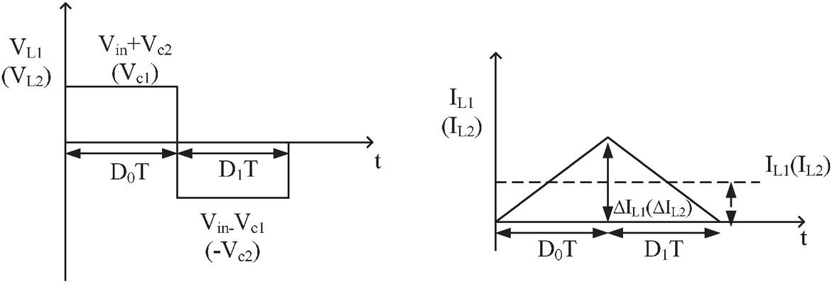
Figure 5 Inductor voltage and inductor current waveforms at boundary conditions.
The steady state inductor current relationship, the capacitor voltages, the input voltage and DC- link voltages with respect to D is obtained by equating our above equations to zero and thus we obtain the (18) [51–53]. Here, qZSI power input is given by P and load resistance is represented by R. The inductor voltages have been analyzed before. We know the current through an inductor lacks the capability of changing instantaneously. Because of this the ST characteristics impart ripple effect in the inductor current. We for analysis have assumed for our system to be in steady state, increase in ripple current that happens in shoot-through state is shown as positive and is equal to decrease in ripple current in non-shoot through state which is negative. If and switching frequency is , and are obtained as (19) and (20) respectively. The voltage across inductors and current through inductors for boundary cases has been shown in Figure 5.
| (18) | ||
| (19) | ||
| (20) |
The boundary inductor current is half the ripple current as given below,
The boundary currents for both the inductors will be given by (21).
| (21) |
Figure 6 Inductor voltage and current waveforms for discontinuous conduction mode.
For the proposed in continuous conduction mode, , for the proposed inverter to work in DCM , Therefore the condition can be established as given in (22) and (23) respectively.
| (22) | ||
| (23) |
Therefore for a known inductance minimum inductor current before DCM starts will be given by (24).
| (24) |
2.5 DCM Operation Analysis
In DCM the steady- state voltage conversion equation used earlier does not hold. For analysis we need to use inductor waveform of DCM. The inductor current thus obtained will be given by (25)
| (25) |
By performing substitutions we obtain the voltage ratio as given in (26).
| (26) |
After the above analysis it is inferred that in DCM, the voltage conversion ratio is dependent on , , L and R. Thus the transition from CCM to DCM depends on resistance and load. Below given are the output current and voltage equations,
for M 1;
Where the minimum value of input voltage is 150 V, therefore we obtain the following values after computation.
Thuson Inverter Bridge, 267 V is the maximum voltage stress. Let the system be of power rating 1 KW.
is maximum current flowing in an inductor. The inductor voltage and current waveforms for discontinuous conduction mode are shown in Figure 6.
2.6 Inductor and Capacitor Selection
For the qZSI inverter working in the boost mode of conversion, the potential maximum interval of the shoot-through state when is calculated as:
If Peak to peak ripple is having value as 20% for the proposed system, the inductance can be calculated as:
From the observations done earlier, capacitor voltage is 250 V. Therefore,
The capacitance of two capacitors is:
Where (assumed). The capacitance of two capacitors is:
Thus,
3 Experimental Setup and Hardware Results
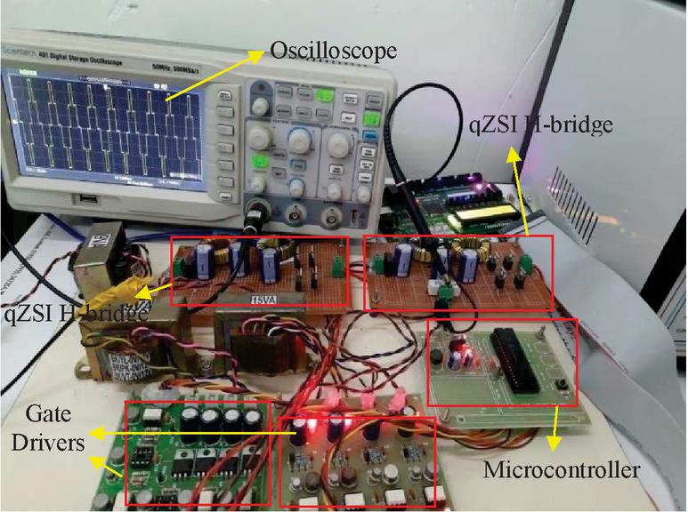
The hardware setup of the presented system is developed to obtain the practical results and all the components have been shown in Figure 7. For proof of the proposed concept, the actual panels have been replaced with dc link voltages and battery system by a resistive load.
Figure 7 Hardware setup.
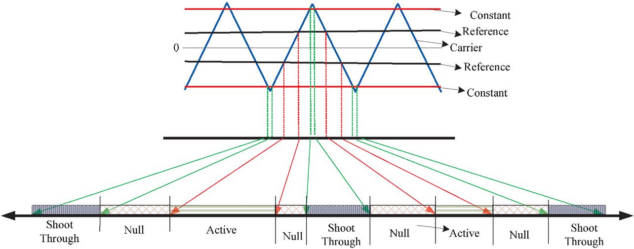
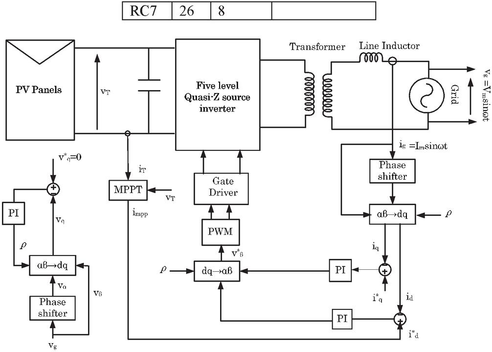
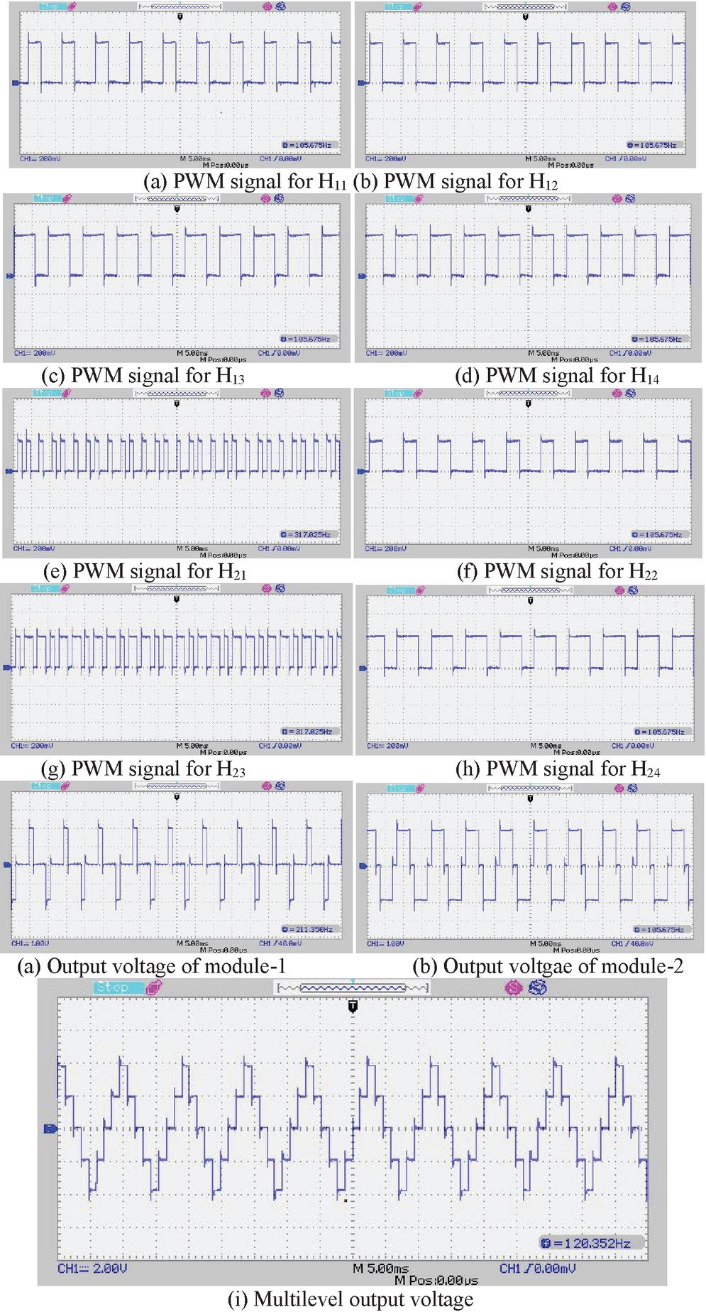
The dspic microcontroller board (PIC16F877A) have been used to generate PWM signal. The dspic signal is provided to gate drives circuit which isolates and amplifies the signals to a suitable value for turning ON the semiconductor switches. The PWM signals with proper ST and NST states have been depicted in Figure 8. The low frequency control is obtained on the basis of the mathematical model done in the paper. The gating signals for individual cells are shown in (6). The stable operation is ensured by adjusting the gain of the controller. The proposed scheme has been implemented in grid connection mode and the complete schematic has been shown in (7). In the proposed scheme, into the grid the current is injected at unity power factor and the harmonics content is minimum. For this purpose there is only -current component (sint) and thus -current component is created for necessary transformations. The transformation into d-q coordinates results into dc component.
Figure 8 PWM signal with ST state and NST states.
Table 2 Pin description in the microcontroller
| Dspic | PIN | Switces | Inverter Bridge |
| RC0 | 15 | 1 | H-bridge-1 |
| RC1 | 16 | 2 | |
| RC2 | 17 | 3 | |
| RC3 | 18 | 4 | |
| RC4 | 23 | 5 | H-bridge-2 |
| RC5 | 24 | 6 | |
| RC6 | 25 | 7 | |
| RC7 | 26 | 8 |
Figure 9 Control system design.
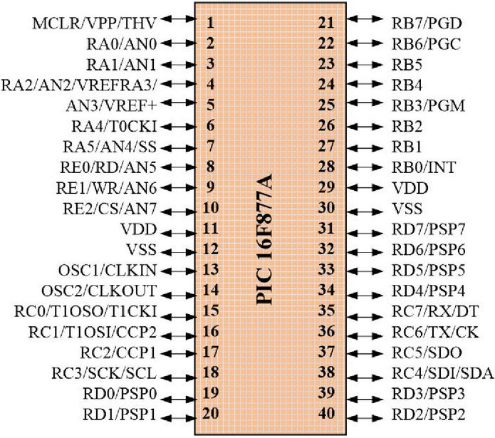
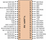
The required angle is chosen between and d-q co-ordinates axes. In order to keep , the value is chosen so that dq-axis aligns with the . Therefore, the and will work as reference and its comparison is done with a triangular signal and on the basis of this logic there is generation of PWM pulses. The ST reference line is adjusted so that the required boost is obtained at the output. Only component is required in this case as and are already known and component is calculated. Here the PV generated power injected in the grid will be proportionate to the current d-axis current as grid voltage is fixed. Hence, the d-axis reference current is fixed and it is obtained from the MPPT algorithm. The control system design is represented in Figure 9 whereas the pin configuration of the microcontroller used in generation of the PWM signal for the semiconductor devices is shown in Figure 10.
Figure 10 Pin configurations of dsPIC micro controller.
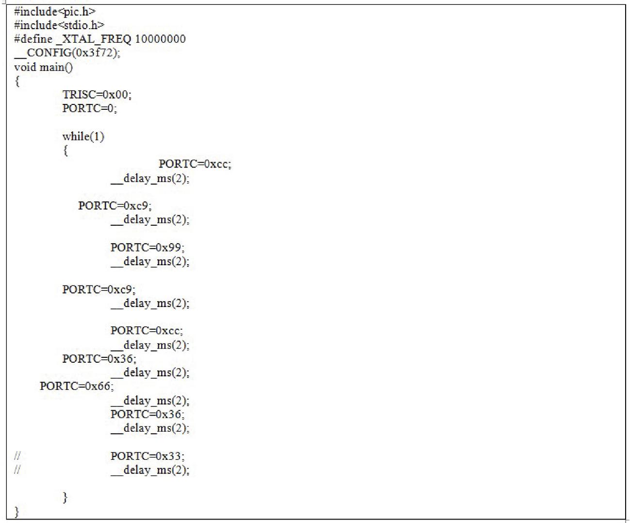
Table 3 Controller code for PWM signal generation
Figure 11 Output gate pulses, module output and multilevel output voltage.
So is nothing but the output current from the MPPT algorithm and it will try to track the d-axis current . The Pin numbers in for generating all the eight PWM pulses is shown in Table 2. The main programme for generating PWM pulses in dspic microcontroller is shown in Table 3. The gate pulses to various semiconductor switches, module output voltage and multilevel output voltage have been shown in Figure 11(a) to Figure 11(i) respectively. The hardware results validate the proposed concept in this paper. The total harmonics distortion has been found in the output waveform is 14.03%.
4 Conclusion
A novel microcontroller based low switching frequency-based pulse width modulation technique for Multi level quasi Z source inverter (qZSI) has been investigated in paper. First the component design of qZSI with continuous and discontinuous operation modes is considered. Then for effective implementation of PIC microcontroller (PIC 16F877A) detailed modeling for qZSI is established for generating the PWM pulses. The five level quasi z-source inverter prototype by having two H-bridge modules have been developed and PWM signals are applied by suitable adjustment of the ST switching states and NST switching state. The proposed algorithm is extremely useful in solar photovoltaic system and application in variable speed drives. The low switching frequency scheme minimizes the switching losses and thus improves the efficiency and reliability of the overall system. The computational and hardware result depicts the effective implementation of the presented scheme.
Acknowledgment
This publication was possible because of SEED gran #IUST/TEQIP/19/36-53 under TEQIP-III project. The statements made herein are solely the responsibility of the author[s].
References
[1] L. García Franquelo, J. Rodriguez, J. I. Leon, S. Kouro, M. d. l. Á. Martín Prats, and R. C. Portillo Guisado, “The age of multilevel converters arrives,” IEEE Industrial Electronics Magazine, 2 (2), 28–39, 2008.
[2] S. A. Gonzalez, S. A. Verne, and M. I. Valla, Multilevel converters for industrial applications. CRC Press, 2016.
[3] J.-S. Lai and F. Z. Peng, “Multilevel converters-a new breed of power converters,” IEEE Transactions on industry applications, vol. 32, no. 3, pp. 509–517, 1996.
[4] S. Kouro, M. Malinowski, K. Gopakumar, J. Pou, L. G. Franquelo, B. Wu, J. Rodriguez, M. A. Pérez, and J. I. Leon, “Recent advances and industrial applications of multilevel converters,” IEEE Transactions on industrial electronics, vol. 57, no. 8, pp. 2553–2580, 2010.
[5] K. K. Gupta, A. Ranjan, P. Bhatnagar, L. K. Sahu, and S. Jain, “Multilevel inverter topologies with reduced device count: A review,” IEEE transactions on Power Electronics, vol. 31, no. 1, pp. 135–151, 2015.
[6] K. K. Gupta and P. Bhatnagar, Multilevel inverters: conventional and emerging topologies and their control. Academic Press, 2017.
[7] S. B. Kjaer, J. K. Pederson, and F. Blaabjerg, “A review of single-phase grid-connected inverters for photovoltaic modules,” IEEE Trans. Ind. Appl., vol. 41, no. 5, pp. 1292–1306, Sep./Oct. 2005.
[8] H. Abu-Rub, A. Iqbal, J. Guzinski, “High Performance Control of AC Drives with Matlab/Simulink Models,” John Wiley and Sons, 2012
[9] F. Z. Peng, “Z-Source Inverter,” IEEE Trans. on Ind. Appl., vol. 39, no. 2, pp. 504–510, March/April. 2003.
[10] Yuan Li, Joel Anderson, Fang Z. Peng and Dichen Liu. “Quasi-Z Source Inverter for Photovoltaic Power Generation Systems,” in Proc. 2009 IEEE Applied Power Electronics Conf., pp. 918–924.
[11] Panda, Anup Kumar, and Richa Pandey. “Performance evaluation of controlled QZSI fed five-phase induction motor under voltage sag and interruption.” International Transactions on Electrical Energy Systems 30, no. 1 (2020): e12166.
[12] Jammy, Ramesh Rahul, and Kirubakaran Annamalai. “A new configuration of seven-level quasi Z-source–based isolated inverter for renewable applications.” International Transactions on Electrical Energy Systems 29, no. 5 (2019): e2833.
[13] Anderson and F. Peng, “A class of quasi-Z-source inverters,” in Proc. IEEE Industry Applications Society Annual Meeting, Oct. 5–9, 2008, pp. 1–7
[14] J. Anderson and F. Z. Peng, “Four quasi-Zsource inverters,” in Proc. IEEE Power Electronics Specialists Conf., PESC, June 15–19, 2008, pp. 2743–2749.
[15] F. Guo, L. Fu, C.-H. Lin, C. Li, W. Choi, and J. Wang, “Development of an 85-kW bidirectional quasi-Z-source inverter with DC-link feed-forward compensation for electric vehicle applications,” IEEE Trans. Power Electron., vol. 28, no. 12, pp. 5477–5488, Dec. 2013.
[16] F. Guo, L. Fu, C.-H. Lin, C. Li, W. Choi, and J. Wang, “Development of an 85-kW bidirectional quasi-Z-source inverter with DC-link feed-forward compensation for electric vehicle applications,” IEEE Trans. Power Electron., vol. 28, no. 12, pp. 5477–5488, Dec. 2013.
[17] M. Zhu, K. Yu, and F.-L. Luo, “Switched inductor Z-source inverter,” IEEE Trans. Power Electron., vol. 25, no. 8, pp. 2150–2158, Aug. 2010.
[18] M.-K. Nguyen, Y.-c. Lim, and G.-B. Cho, “Switched-inductor quasi-Z-source inverter,” IEEE Trans. Power Electron., vol. 26, no. 11, pp. 3183–3191, Nov. 2011.
[19] M. Zhu, D. Li, P.C. Loh, and F. Blaabjerg, “Tapped-inductor Z-Source inverters with enhanced voltage boost inversion abilities,” in Proc. 2nd IEEE Int. Conf. Sustainable Energy Technologies, ICSET, Dec. 6–9, 2010, pp. 1–6,
[20] S. Jiang, D. Cao, and F. Z. Peng, “High frequency transformer isolated Z-source inverters,” in Proc. 26th Annu. IEEE Applied Power Electronics Conf. Exposition (APEC), 2011, pp. 442–449.
[21] Y. Ding and L. Li, “Research and application of high frequency isolated quasi-Z-source inverter,” in Proc. 38th Annu. Conf. IEEE Industrial Electronics Society, IECON, Oct. 25–28, 2012, pp. 714–718.
[22] Liu, Hongpeng, Zichao Zhou, Yuhao Li, Wentao Wu, Jiabao Jiang, and Enda Shi. Impedance Source Inverters. Springer Nature, 2020.
[23] Y. Liu, B. Ge, H. Abu-Rub, and F. Z. Peng, “Modelling and controller design of quasi-z-source inverter with battery-based photovoltaic power system,” IET Power Electronics, vol. 7, no. 7, pp. 1665–1674, 2014.
[24] Y. Li, S. Jiang, J. G. Cintron-Rivera, and F. Z. Peng, “Modeling and control of quasi-z-source inverter for distributed generation applications,” IEEE Transactions on Industrial Electronics, vol. 60, no. 4, pp. 1532–1541, 2013.
[25] Dave, Heema B., Dheerendra Singh, and Hari Om Bansal. “High voltage gain reduced current ripple switched coupled inductor quasi-Z-source inverter.” International Transactions on Electrical Energy Systems 30, no. 4 (2020): e12305.
[26] Li, Tao, and Qiming Cheng. “Structure analysis and sliding mode control of new dual quasi-Z-source inverter in microgrid.” International Transactions on Electrical Energy Systems 29, no. 1 (2019): e2662.
[27] S. Ahmad, M. Al-Hitmi, A. Iqal, I. Ashraf, M. Meraj, and S. Padmanaban. “Low-order harmonics control in staircase waveform useful in high-power application by a novel technique.” International Transactions on Electrical Energy Systems 29, no. 3 (2019): e2769.
[28] S. Ahmad, M. Al-Hitmi, A. Iqbal, K. Rahman, and I. Ashraf. “Low switching frequency modulation of a 3 3 matrix converter in UPFC application using differential evolution method.” International Transactions on Electrical Energy Systems 30, no. 1 (2020): e12179.
[29] Z. L. Liu, and H. Li, “A high-performance photovoltaic module integrated converter (MIC) based on cascaded quasi-Z-source inverters (qZSI) using eGaN FETs,” IEEE Trans. Power Electron., vol. 28, no. 6, pp. 2727–2738, Jun. 2013.
[30] S. B. Kjaer, J. K. Pedersen and F. Blaabjerg, “A review of single-phase grid-connected inverters for photovoltaic modules,” IEEE Trans. On Ind. Appl., vol. 41, no. 5, pp. 1292-1306, Sep./Oct. 2005.
[31] A. Ayad and R. Kennel, “A comparison of quasi-Z-source inverters and conventional two-stage inverters for PV applications,” EPE Journal, vol. 27, no. 2, pp. 43–59, May, 2017.
[32] W. Liang, Y. Liu, B. Ge, H. Abu-Rub, R. S. Balog and Y. Xue, “Double-Line-Frequency Ripple Model, Analysis, and Impedance Design for Energy-Stored Single-Phase Quasi-Z-Source Photovoltaic System,” in IEEE Transactions on Industrial Electronics, vol. 65, no. 4, pp. 3198–3209, April 2018.
[33] S. Ahmad, M. Meraj, A. Iqbal, I. Ashraf, “Selective Harmonics Elimination in Multilevel Inverter by a Derivative free Iterative Method under Varying Voltage Condition”, ISA Transaction, Elsevier, volume 92, pages 241–256, September 2019.
[34] M. Al-Hitmi, S. Ahmad, A. Iqbal, S. Padmanaban and I. Ashraf, “Selective Harmonic Elimination in Wide Range of Modulation Using Modified Newton-Raphson and Pattern Generation Method for Multilevel Inverter” vol. 11, issue 2, 458, MDPI-Energies, 2018.
[35] S. Ahmad, A. Iqbal, I. Ashraf, M.A. Al-Hitmi, “Selected Harmonics Elimination in Multilevel Inverter Using Improved Numerical Technique”, IEEE CPE-PWERENG, Doha, Qatar April 10–12 2018.
[36] S. Ahmad, A. Iqbal, I. Ashraf, R. Alammari, “SHE PWM for Multilevel Inverter Using Modified NR and Pattern Generation for Wide Range of Solutions”, IEEE CPE- PWERENG, Doha, Qatar. April 10–12, 2018. DOI: 10.1109/CPE.2018.8372498.
[37] S. Ahmad, Z. A. Ganie, I. Ashraf, A. Iqbal, “Harmonics minimization in 3-level waveform and its FPGA realization”, IEEE CIPECH, KIET, India. November 1–2, 2018. DOI: 10.1109/CIPECH.2018.8724136.
[38] M. Kumari, M. Ali, S. Ahmad, I. Ashraf, A. Iqbal, M. Tarique “Genetic Algorithm based SHE-PWM for 1- and 3- Voltage source inverters”, IEEE, ICPECA, JMI Delhi, India. November 16–17 2019.
[39] S. Ahmad, A. Iqbal, M. Ali, K. Rahman, A. S. Ahmed, “A Fast Convergent Homotopy Perturbation Method for Solving Selective Harmonics Elimination PWM Problem in Multi Level Inverter”, IEEE Access, volume: 9, pages 113040–113051, August 2021.
[40] S. Ahmad, A. Iqbal, I. Ashraf, and Z. A. Ganie. “Harmonics Minimization in Multilevel Inverter by Continuous Mode ACO Technique.” Innovations in Electrical and Electronic Engineering, pp. 95–104. Springer, Singapore, 2021.
[41] S. Ahmad, and A. Iqbal. “Switching Angles Computations Using PSO in Selective Harmonics Minimization PWM.” In Metaheuristic and Evolutionary Computation: Algorithms and Applications, pp. 437–461. Springer, Singapore, 2021.
[42] Napoles, Javier, Jose I. Leon, Ramon Portillo, Leopoldo G. Franquelo, and Miguel A. Aguirre. “Selective harmonic mitigation technique for high-power converters.” IEEE Transactions on Industrial electronics 57, no. 7 (2009): 2315–2323.
[43] S. Ahmad, I. Khan, A. Iqbal, and S. Rahman. “A Novel Pulse Width Amplitude Modulation for Elimination of Multiple Harmonics in Asymmetrical Multilevel Inverter.” IEEE Texas Power and Energy Conference (TPEC), pp. 1–6., 2021.
[44] N. M. Hoang, and S. Kwak. “Nearest-level control method with improved output quality for modular multilevel converters.” IEEE Access 8 (2020): 110237–110250.
[45] R. Akshay K., J. Holtz, and T. Boller. “Synchronous optimal pulsewidth modulation for low-switching-frequency control of medium-voltage multilevel inverters.” IEEE Transactions on Industrial Electronics 57, no. 7 (2010): 2374–2381.
[46] A. Gambhir, S. K. Mishra and A. Joshi, “Power Frequency Harmonic Reduction and its Redistribution for Improved Filter Design in Current-Fed Switched Inverter,” in IEEE Transactions on Industrial Electronics, vol. 66, no. 6, pp. 4319–4333, June 2019.
[47] M. Meraj, S. Rahman, A. Iqbal and L. Ben–Brahim, “Common Mode Voltage Reduction in A Singlephase Quasi Z-Source Inverter for Transformerless Grid-Connected Solar PV Applications,” in IEEE J. Emerg. Sel. Topics Power Electron. doi: 10.1109/JESTPE.2018.2867521
[48] G. Masoud, S. M. Barakati, and B. Wu. “Extended switched-inductor quasi-Z-source inverter: Modeling and prototype realization.” International Transactions on Electrical Energy Systems 29, no. 3 (2019): e2744.
[49] S. Ahmad, R. Uddin, Z. A. Ghanie, and A. Tasneem. “Close Loop Control of quasi Z-Source Inverter in Grid Connected PV System.” In 2019 International Conference on Electrical, Electronics and Computer Engineering (UPCON), pp. 1–6. IEEE, 2019.
[50] Y. Gu, Y. Chen, and B. Zhang, “Enhanced-boost quasi-Z-source inverter with an active switched Z-network,” IEEE Trans. Ind. Electron., vol. 65, no. 10, pp. 8372–8381, Oct. 2018.
[51] Y. Liu, B Ge, H. Abu-Rub, ‘Phase-shifted pulse-widthamplitude modulation for quasi-Z-source cascade multilevel inverter based photovoltaic power system’, IET Power Electron., vol. 28. no. 7, pp. 1444–1456, 2014.
[52] Liu, Yushan, Haitham Abu-Rub, Baoming Ge, Frede Blaabjerg, Omar Ellabban, and Poh Chiang Loh. Impedance source power electronic converters. John Wiley & Sons, 2016.
[53] S. Ahmad, A. Iqbal, M. Ali, K. Rahman, and A.S. Ahmed “A Fast Convergent Homotopy Perturbation Method for Solving Selective Harmonics Elimination PWM Problem in Multi Level Inverter.” IEEE Access 9, 113040-113051. 2021
Biographies

Salman Ahmad received the B.Tech degree in Electrical Engineering from Aligarh Muslim University, Aligarh, India, in 2010 and M.Tech degree from Indian Institute of Technology, Roorkee, India, in 2012, the Ph.D. degree from Aligarh Muslim University, India in 2020. He is currently an Assistant Professor of electrical engineering with Islamic University of Science and Technology Awantipora, India. He has published more than 25 technical papers in different journals and conference proceedings and contributed three book chapters in edited books published by Elsevier USA and Springer Nature Singapore respectively. He received 4 research grants from various government agencies. His current research interests include Power converters, PWM techniques, multilevel and multiphase converter, variable speed drives and renewable energy systems.

Rahim Uddin received the BE degree in Electrical Engineering from RTM Nagpur University in 2013 and M Tech degree in Power electronics from NIT Calicut in 2017. He was working as assistant professor at Islamic university of science and technology Awantipora under TEQIP-III. He is pursuing Phd from NIT Srinagar. His research interests include high power converters and multilevel topology and ac-dc matrix converters.

Zahoor Ahmad Ganie received the B.E degree in Electrical Engineering from University of Jammu, Jammu and Kashmir, India, in 2006, M. Tech degree in Electrical Power and Energy Systems from National Institute of Technology, Srinagar, Jammu and Kashmir, India in 2017. Currently, he is an Assistant Professor in the Department of Electrical Engineering, Islamic University of Science and Technology, Awantipora, India. His research interests include Pulse Width Modulation, Electric Machine Drives, modeling and control of Voltage Source Inverters, Multilevel inverters, power semiconductor devices.

Ahmed Sharique Anees received the Ph.D. degree in Electrical Engineering from Jamia Millia Islamia, New Delhi, India, in 2017. Currently, he is an Assistant Professor in the Department of Electrical Engineering, Islamic University of Science and Technology, Awantipora, India. He has been awarded two sponsored research projects in the area of renewable energy systems, Ground source heating system and published/presented more than 14 research papers in reputed international and national journals and conference proceedings. His research interests include solar photovoltaic, renewable energy and distributed generation.

Farhad Ilahi Bakhsh received Diploma and B. Tech degree in Electrical Engineering from Aligarh Muslim University (AMU), Aligarh, India in 2006 and 2010, respectively. He was awarded University Medal (Gold) for standing first throughout Diploma in Electrical Engineering. He has been awarded first position in SPOTLIGHT and third position in overall solar conference during cognizance 2010 in Indian Institute of Technology Roorkee. Then he pursued Masters in Power System and Drives from the Aligarh Muslim University. In Masters he secured first position in his branch. He delivered a number of Keynote talks, at National and International level in conferences, workshops, STC, etc. He has more than 50 published papers in International reputed Journals, International and National reputed Conferences. He has two granted patent in his credit. His research area of interests includes Performance Analysis of Variable Frequency Transformer and Application of Power Electronics in Renewable Energy Systems.
Distributed Generation & Alternative Energy Journal, Vol. 37_4, 929–958.
doi: 10.13052/dgaej2156-3306.3743
© 2022 River Publishers
