Control and Power Management Strategy for Shunt DC Electric Spring Integrated DC Microgrid
A. G. Anu*, R. Harikumar and S. Ushakumari
Department of Electrical Engineering, College of Engineering Trivandrum, APJ Abdul Kalam Technological University, Kerala, India
E-mail: aganu@cet.ac.in
*Corresponding Author
Received 15 July 2021; Accepted 16 December 2021; Publication 24 May 2022
Abstract
Incorporation of intermittent renewable sources and nonlinear loads to DC microgrid (DCMG) has increased its vulnerability to voltage instability and flicker. An innovative Demand Side Management (DSM) program that can help in mitigating these voltage disruptions is the deployment of DC Electric Spring (DCES) technology. In this regard, this paper focuses on small signal modeling and controller design of shunt DCES (ShDCES) in DCMG. The test system comprises of an MPPT controlled Solar Photo-Voltaic (SPV) system, battery-operated DCES and various loads. The MATLAB / Simulink performance analysis of the system indicates that, with the incorporation of power management strategy, the ShDCES configuration has enhanced the power quality of SPV-fed DCMG with fast dynamic response in comparison with its “series” counterpart. The effective utilization of battery operated DCES on the load side, instead of the source side, makes it less battery dependent, resulting in enhancement of battery life and lesser environmental hazards. The simulation results are also validated using real-time simulator OP4510 RTS.
Keywords: DC microgrid, shunt DC Electric Spring, PI controller, power management strategy.
1 Introduction
In the last few decades, there has been an increased urge to reduce carbon footprint by utilizing the increased penetration of renewable energy sources in the modern grid, which has lead to grid instability and poor power quality. The use of microgrids could be beneficial to get rid of these drawbacks. Generally, microgrids are categorised as AC, DC and hybrid AC-DC microgrids [1, 2, 3, 4, 5, 6].
It was Thomas Alva Edison who first tried the concept of DC grid in 1882. However, this concept failed to gather momentum owing to excessive transmission losses at low DC voltages. The need for conversion to higher voltages and lack of technologies for DC voltage conversion has eventually resulted in the alternating current systems innovated by Tesla to take over DC network [4, 5, 7]. Now, it is the most appropriate time to return to the DCMG concept owing to the tremendous advancement in power electronics and increase in demand for remote onsite generation via renewable energy sources(RESs). Also, the bottlenecks faced by Edison’s DC grid are no longer relevant due to RESs, present-time electronic appliances and all storage devices being DC in nature, eliminating the requirement for reactive power compensation, synchronization and additional power conversion stages [5, 7, 8, 9]. This makes the DCMG a viable substitute for AC grid in today’s world, particularly to small scale residential applications where remote onsite generation is an option. Furthermore, it might even be a favourable choice to extend a feasible, inexpensive and dependable solution for isolated electrification projects in rural areas. Thus the DCMG has turned out to be one of the most preferred alternative for remote power delivery. Despite these advantages, DCMGs are susceptible to voltage flickers and instability owing to the integration of non-dispatchable renewable energy sources, nonlinear loads, and occasional faults [8, 9, 10, 11, 12, 13]. The primary challenge faced by the DCMG is the need to maintain dynamic voltage regulation as today’s electronic loads are intolerant to voltage changes and also the stability of a DCMG is indicated by its constant bus voltage.
The stability of any power system depends heavily on the balance between supply and demand. Conventional power system follow a power generation based strategy rather than being load dependent [10, 11]. As it is impractical to determine real-time generation due to the intermittent nature of RESs, it would be preferable to shift to demand oriented power control strategy [12, 13, 14]. Battery is one of the alternative to achieve real time instantaneous energy balance, but prohibitive costs of batteries and the environmental hazards from disposal of defunct batteries are the major challenges [15, 16].
Electric Spring (ES) is a newly proposed concept to reduce the battery requirement and to enhance the stability of the DC grid having non-dispatchable renewable energy sources with altering characteristics. The objective of prior research has mainly been on the use of ES in AC power systems [17, 18, 19]. The ES is a switched mode voltage converter usually connected in series with Non-Critical Loads (NCL) for grid stabilization functionalities against disturbances arising from integration of renewable resources in AC systems [17]. Inclusion of storage elements to ES configuration extended its functionalities to include storage reduction [20, 21, 22], three phase balancing etc [23] and frequency stabilization [24].
Present-day research has concentrated on exploring the feasibility of SDCES as a smart load cascaded with deferable loads [25, 26, 27, 28, 29, 30]. One missing element in these researches has been voltage tolerance limit of the NCLs. As a result, practical implementation of SDCES configuration is not possible without a proper power management scheme with load shedding. At the same time SDCES has a slow response compared to its shunt counterpart [26, 31]. So, this work focuses on the feasibility of using ShDCES configuration on low voltage DCMGs in conjunction with the incorporation of a power management strategy. Both the simulation and experimental study in an SPV fed DCMG test system have revealed the efficacy of ShDCES in improving the dynamic voltage regulation and lengthening the lifetime of battery storage. Contributions to the work are summarized as follows:
1. A detailed small signal modeling and controller design procedure for ShDCES integrated DCMG are developed.
2. A power management strategy for the efficient utilization of ShDCES in DCMG is proposed. The proposed method effectively manipulates the NCL to enhance the charge/ discharge cycle of battery.
3. The proposed power management strategy and selected controller parameters are verified using simulation as well as OP4510 RTS real time environment.
The remaining sections are structured as follows. The Section 2 deals with system configuration and modeling which includes the basic concept, design and operating modes of DCES, PV design and system loads. Section 3 covers controller design and power management strategy of SPV-fed ShDCES integrated DC microgrid test system. The simulation studies, experimental validation and conclusions are detailed in Section 4, Section 5 and Section 6 respectively.
2 System Configuration and Modeling
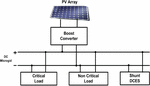
The generalized block diagram of the test system is as depicted in Figure 1. The system basically includes MPPT controlled SPV system, ShDCES and loads. The loads and sources are interfaced to the DC bus via converters. The battery operated ShDCES is connected in parallel with the loads to meet demand during shortfall in PV generation. A control strategy together with a power management strategy is proposed to ensure DC bus voltage stabilization during source-side and load-side disturbances.

Figure 1 Generalised block diagram.
Similar to mechanical springs that are capable of storing and releasing equivalent energy to create a force by averting the displacement from normal, ES brings about boost or buck in voltage based on system necessity. The term ES has been coined from the irrefutable force-voltage analogy in control system engineering [26].
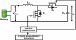
The DCES utilizes a battery and a single legged bidirectional DC-DC converter which can operate in buck and boost mode as depicted in Figure 2. The supply-side voltage variation triggers the DCES into action for maintaining a constant voltage across NCL, by injecting or absorbing a suitable voltage to or from the ES, in order to maintain power balance automatically. It is obvious from the findings that DCES could play a major role in minimizing battery storage requirements in smart grid as well as reducing charging/discharging cycles of batteries.
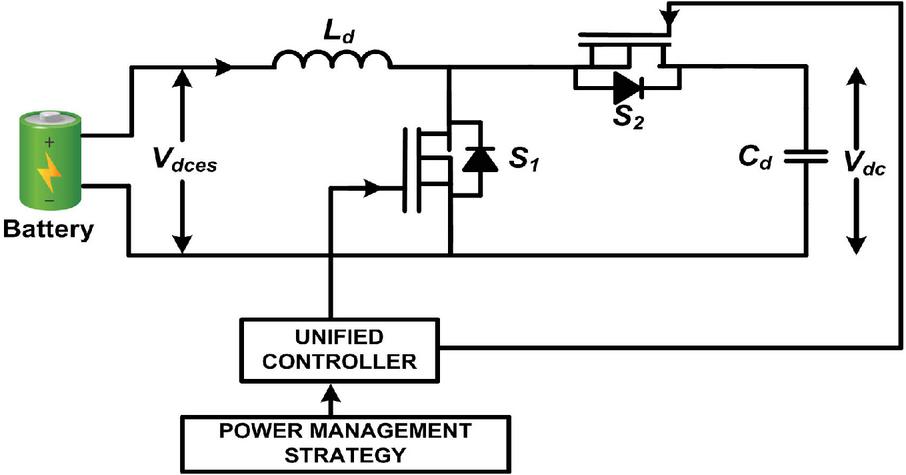
Figure 2 Basic configuration of DCES.
Depending on the operating principle, there are two categories of DCES, namely SDCES and ShDCES [26, 27, 28]. Both SDCES and ShDCES are DC-DC converters with storage devices operating in synchronisation with voltage controller circuit for accomplishing stabilized DC bus voltage. The SDCES plays the role of a controllable voltage source to form a smart load when cascaded with NCL [17, 26]. When the bus voltage is above reference value, current is absorbed to raise the NCL voltage, while buck operation is initiated to release current when the bus voltage drops below the reference value. The ShDCES acts as a controllable current source shunted with the DC bus [26]. When the bus voltage surpasses its reference value, the DCES draws current from the bus whereas it releases current to the bus when the bus voltage gets below the reference value. ShDCES maintains a consistent voltage across all the loads attached to the bus [17, 26] as opposed to SDCES, which regulates bus voltage by relinquishing the voltage quality of NCL. Hence, this work has proceeded with shunt type configuration and Figure 2 depicts the basic circuit of ShDCES.
2.1 Operating Modes of DCES
The modes of operation of DCES are grouped into four categories [8, 9, 10, 11, 12, 23]:
1. Boosting Discharge Mode (BDM): When the source voltage drops below the desired value, DCES initiates a discharge from the battery resulting in boosting bus voltage to reinstate system stability.
2. Boosting Charge Mode (BCM): This mode is triggered and operated similarly to the BDM. The additional power is utilised to initiate the charging mode of battery.
3. Suppressing Discharge Mode (SDM): In this mode, when bus voltage ascends the desired value, DCES initiates battery to discharge and transfer extra power to the bus thus stepping down the bus voltage.
4. Suppressing Charge Mode (SCM): The SCM is similar to SDM but the additional power is utilized to charge the battery instead of delivering to the bus.
The operating modes of SDCES include BDM, BCM and SCM whereas ShDCES operates only in BDM and SDM [26, 29, 30, 31].
2.2 Design of ShDCES
The design of ShDCES comprising of a single legged bidirectional DC-DC converter topology operating in buck and boost mode is briefly presented. The bidirectional converter consists of an input port and output port. A battery is connected to the input port and the output port is connected to the DC bus which also links the MPPT controlled SPV module. When it is operating in boost mode, switch S1 conducts at the specified duty cycle whereas, the internal diode of S2 is engaged during the complimentary cycle [32, 33, 34, 35]. Similarly during buck mode, switch S2 is brought to conduct at needed duty cycle while the internal diode of S1 gets into action during complimentary cycle. The equations found in [33] are used in the design of passive components of ShDCES assuming continuous conduction mode of operation.
| (1) | ||
| (2) | ||
| (3) |

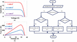
Figure 3 (a) I-V Characteristics (b) P-V characteristics of PV panel with varying irradiance (c) P & O MPPT algorithm flow chart.
2.3 PV Design
Modeling of PV arrays are detailed in several literatures [36, 37, 38]. PV modules are cascaded and/or shunted forming PV arrays to match the needed voltage and current. The temperature and irradiation variation strictly affects the PV array’s characteristic curves. Figures 3(a) and 3(b) indicate I-V and P-V curves of the PV array used for simulation. Figure 3(c) depicts the flow chart of Perturb and Observe (P&O) algorithm used for the MPPT controller [39]. PV specifications are listed in Table 1. Equation (4) represents the characteristic equation of single diode model of PV array.
| (4) |
Where: : PV array voltage : PV array current : Total photo-current generated from PV array : Reverse saturation current of PV cell & : Series and parallel resistances A: Diode ideal factor T: PV cell’s working temperature K: Boltzmann’s constant (1.381023J/k) : Total number of Parallel connected PV cells : Total number of series connected PV cells.
Table 1 The system parameters for simulation
| S.No | Parameters | Values |
| 1 | PV Parameters | |
| Open Circuit Voltage () | 38.6 V | |
| Short Circuit Current () | 8.93 V | |
| Voltage at MPP () | 31.6 V | |
| Current at MPP () | 8.21 V | |
| Power at MPP () | 259.4 W | |
| 2 | DCES Parameters | |
| DCES Voltage () | 24 V | |
| DCES Ah Capacity | 17 Ah | |
| DCES Inductance () | 2.2 mH | |
| DCES Capacitance () | ||
| Switching Frequency () | 20 kHz | |
| 3 | Load Parameters | |
| Critical Load Resistance () | 20 | |
| Non Critical Load Resistance () | 20 | |
| Nominal Load Power | 0.5 kW | |
| Bus Voltage () | 48 V |
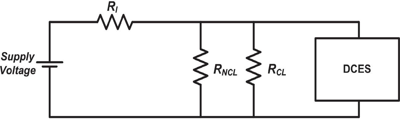
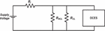
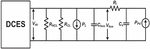
Figure 4 Basic circuit of ShDCES.
2.4 System Loads
Electrical loads are differentiated as Critical Loads (CL) and Non Critical Loads (NCL) based on its tolerance limit for voltage [26]. CL includes appliances such as data servers and computers which require a constant DC voltage whereas includes devices like washing machines, electric water heater and air conditioners which can withstand wider variations in DC voltage but within an admissible range [26]. This paper focuses on ShDCES configuration where represents critical load and represents noncritical load as depicted in Figure 4. The represents the parallel combination of and as the proposed system for analysis is ShDCES.
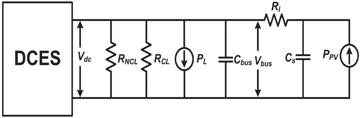
Figure 5 ShDCES integrated SPV Fed DC microgrid.
3 Controller Design and Power Management Strategy
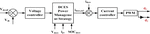
A single bus ShDCES integrated DC microgrid as shown in Figure 5 is proposed in this paper. The control as well as power management strategy adopted for ShDCES is as shown in Figure 6. The control strategy regulates the bus voltage and ShDCES current. The power management strategy (PMS) decides the operating mode of ShDCES under load and source side variations. The ShDCES current is regulated by current loop and the bus voltage is regulated by voltage control loop. The small signal modeling and analysis done for the selection of controller parameters are detailed in Section 3.1.
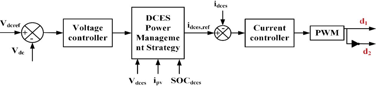
Figure 6 Control and Power management strategy.
3.1 Small Signal Modeling and Stability Analysis of ShDCES
The linearized Equations (5) and (6) of ShDCES are derived assuming constant DCES voltage and small signal modeling procedure and are used to derive the corresponding control transfer functions.
| (5) | |
| (6) |
The expressions for DC voltage to DCES current transfer function ( (s)), DC voltage to duty cycle transfer function () and DCES current to duty cycle transfer function () of ShDCES are given in Table 2.
Table 2 The SSM based controller transfer functions
| (a) | Control to voltage transfer function |
| (b) | Control to voltage transfer function |
| (c) | Current to voltage transfer function |
3.2 Controller Parameter Design
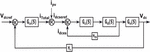
A dual loop control methodology comprising an inner current control loop and outer voltage control loop as shown in Figure 7 is adopted in this paper. The current control loop is designed with a larger bandwidth to operate the voltage control loop independent of current control loop thereby simplifying the design of voltage control loop.
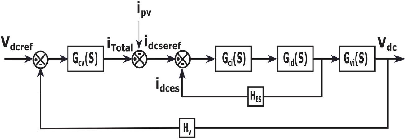
Figure 7 Small signal model of ShDCES integrated DC microgrid.
3.2.1 Inner Current Loop Controller
The inner current control loop for the DCES is designed using the control transfer function represented in Table 2. To ensure stability, a bandwidth of 10 krad/sec and 60 phase margin is chosen to design the controller of the current control loop of DCES. () represents the open-loop transfer function of DCES current control loop and is expressed as follows:
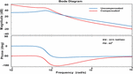
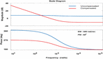
and represents the proportional and integral gain for the DCES current control loop respectively. denotes the feedback gain of DCES current control loop. The Bode plot of the DCES current control loop with and without compensator is shown in Figure 8. The controller parameters are designed using the SISO toolbox in MATLAB and the values obtained are and .
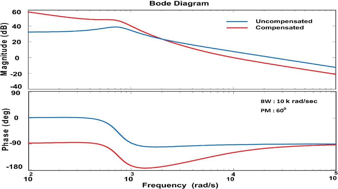
Figure 8 Bode plot of uncompensated and compensated current control loop.
3.2.2 Outer Voltage Control Loop
The transfer function represented in Table 2 is used for calculating which is the voltage loop’s open-loop transfer function. The is obtained as follows: The feedback gain for the overall voltage control loop is represented as . Figure 9 represents the Bode plot of the uncompensated and compensated open-loop transfer function for voltage control loop. The controller parameters are designed to meet a bandwidth of 600 rad/sec and a phase margin of 60 using the SISO toolbox in MATLAB so that the system stability of outer voltage control loop is ensured. The designed parameters for the outer voltage control loop are and .
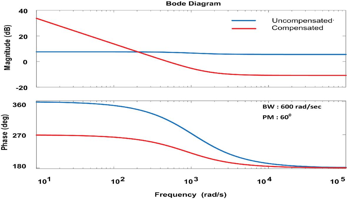
Figure 9 Bode plot of uncompensated and compensated outer voltage control loop.
3.3 Power Management Strategy
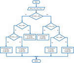
The proposed Power Management Strategy (PMS) aims at ensuring efficient operation of ShDCES by accommodating both load power demand and SoC range of DCES. The unified controller of ShDCES operates in relation to power availability in the DC bus. However, a PMS is required to control the charge and discharge cycles of ShDCES, thereby ensuring increased battery life. The power flow in NCL and CL can also be controlled using the proposed PMS.
The proposed PMS controls the operation of NCL by measuring the power demand and SOC of ShDCES. The flowchart of proposed PMS is illustrated in Figure 10. and are the upper and lower limit of ShDCES power demand. If the ShDCES power demand is greater than , the CL power demand is met by sacrificing the NCL whereas lower limit enables the reverse power flow from DC bus. The operation of ShDCES is determined by the availability of PV power, if the power demand lies between upper and lower limit. This aids in extending the operating hours and life span of battery operated ShDCES.
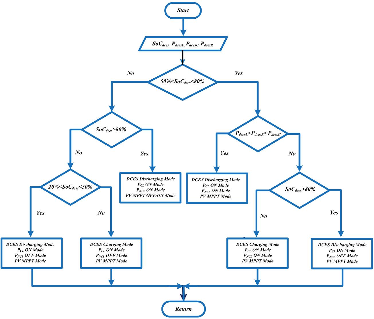
Figure 10 Flow chart of Power management strategy of ShDCES.
The DCES operation is designed based on available SoC and load demand. The modes are explained as follows:
i >80%: In this mode, the stored energy in ShDCES is at its maximum allowable limit. Charging is limited and supplying to the load is preferred. Hence, NCL and CL are active and PV shifts to load regulation mode to supply the load demand. If the PV generation is less than load power demand then ShDCES meet the deficit power of CL.
ii : In this mode, the ShDCES can supply or absorb energy depending on the load demand. In this range, the ShDCES would have enough power to meet the total load demand. This mode is divided into two sub modes so as to control the operation of NCL and CL. If the power demand to the ShDCES is greater than , then NCL is disconnected to support the power demand of CL. On the other hand, if the power demand is less than the upper limit allowed, the ShDCES operates to supply or absorb power from DC bus.
iii : In this mode,the of ShDCES lies in between . Hence, the NCL is disconnected to fully utilize the ShDCES for CL power demand. Also, the PV operates in MPPT mode.
iv : If the is less than 20%, the NCL is disconnected and the operation of CL and DCES are determined by the PV power availability. If there exist excess PV generation after meeting CL demand the DCES absorbs the excess power to regain its SoC. If the PV generation is not sufficient to meet the CL demand, PV control shifts to load regulation mode. Load regulation is not discussed as the focus of the work is on ShDCES. Preference of this mode is to charge the ShDCES and helps in restoring the normal operation of the system.
4 Simulation Results and Discussions
Extensive simulation to validate the efficacy of the proposed scheme were conducted. The simulation parameters are shown in Table 1. The maximum PV power is set as 0.5 kW. The and are set as 100 W and 0 W respectively. Total CL power demand is 400 W. The system was tested under various source and load disturbances.
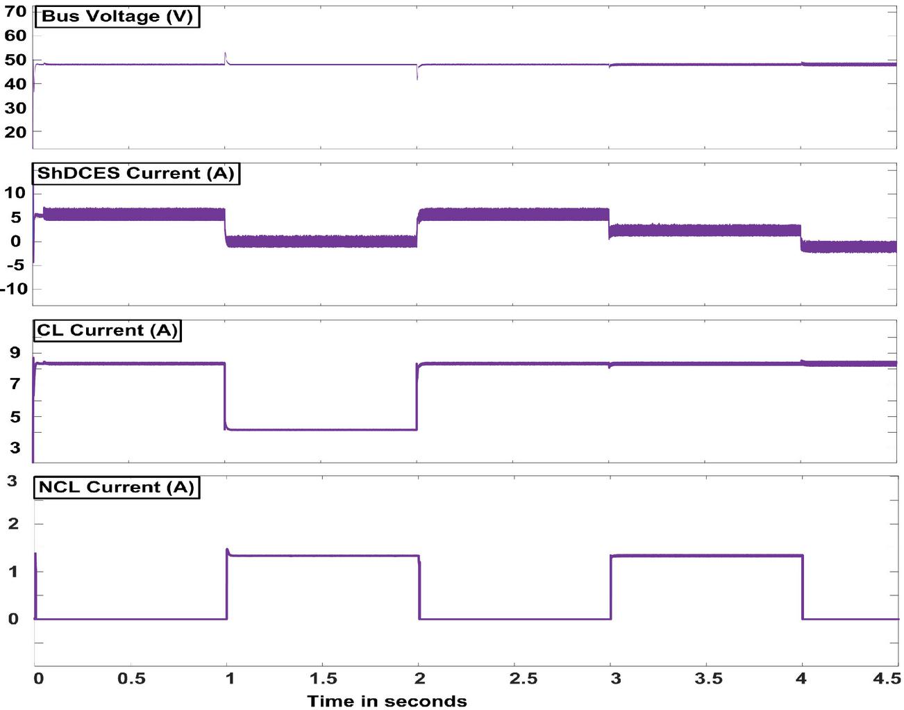
Figure 11 The DC bus voltage, ShDCES Current, CL current and NCL current.
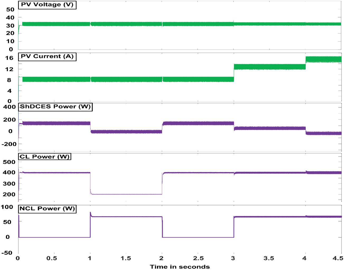
Figure 12 The PV voltage, PV current, ShDCES power, CL power and NCL power.
4.1 System Response to Load Disturbances
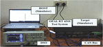
The performance evaluation of the proposed control and PMS of ShDCES was carried out under load disturbances in MATLAB / Simulink. Figure 11 shows the DC bus voltage, CL current, NCL current and ShDCES current. In the case study, load disturbances are applied at instances t 1 sec and t 2 sec. From time interval t 0 to t 1 sec, the CL load demand is 400 W and PV generation is 260 W only. As per the PMS, the PV source and ShDCES operate together for supplying the CL and the NCL is deactivated to make the system less battery dependent. i.e. the ShDCES operates in boost mode to supply the deficit of 140 W to meet CL demand. To analyse the coordinate operation of ShDCES, NCL and PV source, the CL connected to the system was reduced to 200 W at t 1 sec and then reverted back to 400 W at t 2 sec. The reduction in load demand is reflected as a reduction in ShDCES current resulting in the activation of the NCL, so that PV source and ShDCES can supply NCL and CL simultaneously. The waveforms depict that the DC bus voltage is regulated constant with faster dynamic response even during load disturbances. The waveforms in Figures 11 and 12 ensure that the proposed PMS makes the system less battery dependent and the life cycle of battery in ShDCES configuration is prolonged by reducing its charging/discharging cycle. The PV voltage, PV current, ShDCES power, CL power and NCL power shown in Figure 12 validate the power sharing. Figure 13 depicts the experimental set up of the test system. The results obtained from real time simulator shown in Figure 14 validate the effectiveness of the proposed system.
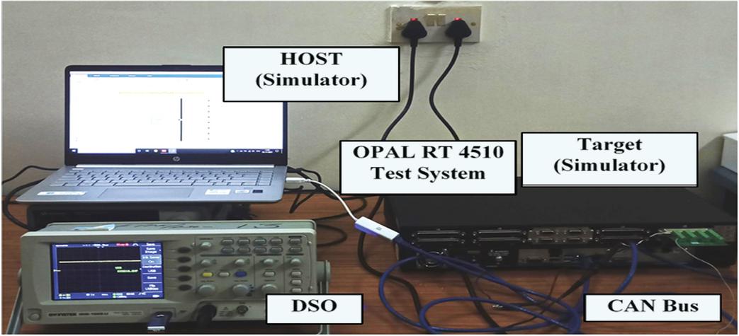
Figure 13 Experimental set up for real time study.
4.2 System Response Under Variation in PV Source
The performance evaluation of the proposed control and PMS of ShDCES under variation in PV source is analysed in this section. The variation in PV power enables ShDCES to operate in two modes in a DCMG environment. When the total load demand exceeds PV power generation, the ShDCES operates in boost mode to supply the deficit power to meet the load demand. This is shown between instances t 3 sec and t 4 sec in Figure 11. If the power available from PV generation is more than CL power demand, NCL is activated. From t 4 sec to t 5 sec, the PV generation is increased such that the total PV power is more than sum of CL and NCL power demand. Thus both NCL and CL are active simultaneously and surplus power is used to charge ShDCES by operating in buck mode. Figure 12 shows the power sharing of PV source, ShDCES, CL and NCL.
The simulation study reveals that the disconnection of NCL at the time of excess power demand ensures the smooth operation of CL and ShDCES. Whenever the CL power demand exceeds PV power, the NCL is connected or disconnected based on the available power of ShDCES. Hence the proposed PMS ensures reduced battery storage requirement as the reduction in PV power generation results in the disconnection of NCL for meeting the CL load demand.
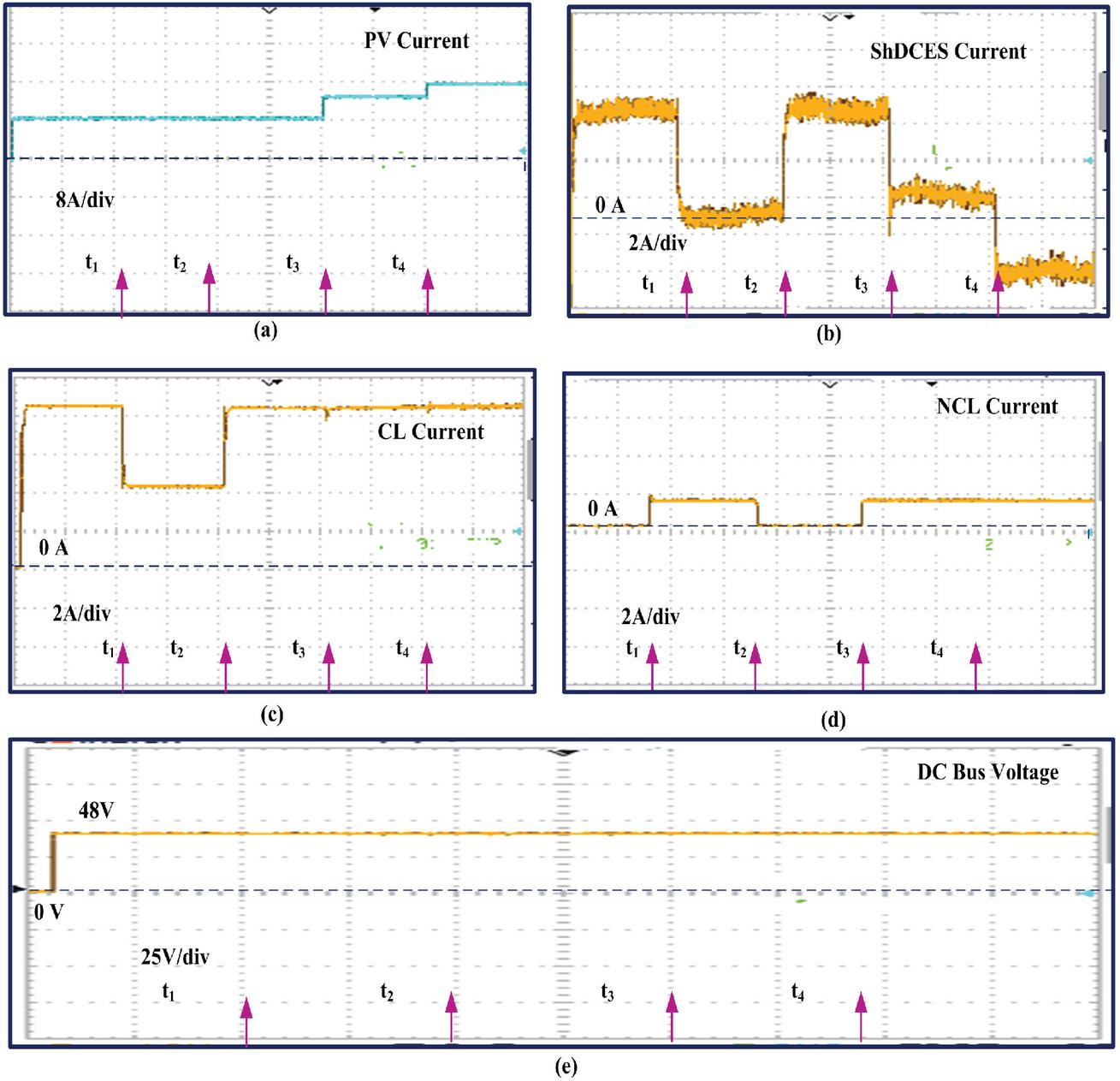
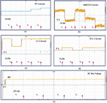
Figure 14 (a) PV current (b) ShDCES Current (c) CL current (d) NCL current (e) DC bus voltage.
5 Experimental Study and Discussions
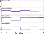
A real-time simulation study using the OP4510 RTS simulator is conducted to validate the MATLAB simulation results. The control method is included in the control block of Matlab/Simulink® and real-time simulations were performed using the FPGA-based real-time simulator as shown in Figure 13. System parameters considered for experimental evaluation are similar to those for simulation studies and are shown in Table 1. The performance evaluation of the proposed controller and PMS of ShDCES under variation in load and PV source are experimentally validated. Experimental results of PV current, SHDCES current, CL current, NCL current and DC bus voltage are depicted in Figure 14.
To analyze DCMG performance corresponding to load variation, CL power is reduced to 200 W at which is reflected as a reduction in CL current to 4 A as depicted in Figure 14(d). According to the PMS, the NCL has activated which in turn increases the NCL current to 2 A as the load demand is less than 20% of the rated load. At CL current reinstates to 8.3 A as depicted in Figure 14(c). In this case, the NCL is deactivated according to the PMS and ShDCES begins to supply the power difference to maintain critical load voltage stability which is reflected as 0 A for NCL as depicted in Figure 14(d). In all of the above cases, the DC bus voltage is regulated at 48 V irrespective of the load variations which validates the effectiveness of the proposed system.
When the total load demand exceeds PV power generation, the ShDCES operates in boost mode to supply the deficit power to meet the load demand. This is shown between instances and in Figure 14(b). If the power available from PV generation is more than CL power demand, NCL is activated. As depicted in Figure 14(a) at instances and , the PV generation is increased such that the total PV power is more than the sum of CL and NCL power demand. Thus both NCL and CL are active simultaneously as depicted in Figures 14(c) and 14(d) and surplus power is used to charge ShDCES by operating in buck mode as in Figure 14(b). In all the above mentioned scenarios, the CL voltage is kept constant and the ShDCES balances the maximum power generated by PV and load demand.
The real-time manipulation of the NCL reduces the battery’s charge/discharge rate and thereby increases the cycle life of the battery. The response of system operation with PV variations and load disturbances validate the coordinate operation of ShDCES and PMS in regulating bus voltage which in turn enhances DCMG stability.
6 Conclusion
The rapid increase in electronic loads, renewable generation units, and electric vehicles has created a galaxy of opportunities for the DCMG to play a pivotal role in future power dispatch in an exponential way. The integration of nonlinear loads and renewable sources could lead to power quality and stability issues in DCMGs. The proposed control and PMS for the ShDCES configuration presented in this paper ensure DC bus voltage stabilization with faster dynamic response during fluctuating irradiance and load-declining circumstances. The proposed PMS also makes the system less battery dependent and extends the life cycle of the battery in ShDCES configuration by reducing charging/discharging cycles. Both the simulation and experimental results have substantiated that the utilization of ShDCES can reduce the power quality issues and environmental concerns prevailing in stand-alone DCMGs to a certain extent. The future scope of the work includes the development of a new controller other than conventional PI controller which may further enhance the stability of ShDCES integrated DCMG.
References
[1] R. H. Lasseter and P. Paigi, “Microgrid: a conceptual solution”, 35th Annual Power Electronics Specialists Conference (IEEE), 2004.
[2] R. M. Elavarasan et al., “A Comprehensive Review on Renewable Energy Development, Challenges, and Policies of Leading Indian States With an International Perspective,” IEEE Access, Vol. 8, pp. 74432–74457, 2020.
[3] J.J. Justo, F.Mwasilu, J. Lee, J.W. Jung, “AC-microgrids versus DC-microgrids with distributed energy resources: A review”, Renewable and Sustainable Energy Reviews, Vol. 24, pp. 387–405, 2013.
[4] A. El-Shahat, S. Sumaiya, “DC-Microgrid System Design, Control, and Analysis”, Electronics, Vol. 8(2), 2019.
[5] T. Dragicevic, X. Lu, J. C. Vasquez, and J. M. Guerrero, “DC grids Part II: A review of power architectures, applications, and standardization issues”, IEEE Transactions on Power Electronics, Vol. 31(5), pp. 3528–3549, 2016.
[6] R. HariKumar, S. Ushakumari, “A Novel Architecture for Data Management and Control in Autonomous Intelligent Microgrid”, Procedia Computer Science, Vol. 89, pp. 412–421, 2016.
[7] A. Sannino,G. Postiglione and M. H. J. Bollen, “Feasibility of a DC network for commercial facilities”, IEEE Transactions on Industrial Applications, Vol. 39(5), pp. 1499–1507, 2003.
[8] H. Kanchev, D. LuF, ColasV, Lazarov and B. Francois, “Energy management and operational planning of a microgrid with a PV-based active generator for smart grid applications”, IEEE Transactions on Industrial Electronics, Vol. 58(10), pp. 4583–4592, 2011.
[9] Rana Abou Hashem et al., “Design of an electric spring for power quality improvement in PV based DC grid”, 2018 IEEE Symposium on Computer Applications and Industrial Electronics, (ISCAIE), 2018.
[10] K. T. Mok, M. H. Wang, S. C. Tan and S. Y. R. Hui, “DC Electric Springs A Technology for Stabilizing DC Power Distribution Systems”, IEEE Transactions on Power Electronics, Vol. 2(2), pp. 1088–1105, 2017.
[11] A. G. Anu, R. Harikumar , S. Ushakumari, “Power Quality Enhancement of DC Micro-Grid Using DC Electric Spring”, Advances in smart Grid Technology, Lecture Notes in Electrical Engineering book series LNEE, Vol. 687, Springer, pp. 137–148, September 2020.
[12] D. Moeini, A. Chandra and A. Kaymanesh, “Application of DC Electric Spring in Modern DC Microgrids, Review and Proposition”, 2021 IEEE Electrical Power and Energy Conference (EPEC), pp. 28–32, 2021.
[13] E. Hossain, M. R. Tür, S. Padmanaban, S. Ay and I. Khan, “Analysis and Mitigation of Power Quality Issues in Distributed Generation Systems Using Custom Power Devices”, IEEE Access, Vol. 6, pp. 16816–16833, 2018.
[14] P. Palensky and D. Dietrich, “Demand side management: Demand response intelligent energy systems and smart loads”, IEEE Transactions on Industrial Informatics, Vol. 7(3), pp. 381–388, 2011.
[15] A.G. Olabi, C. Onumaegbu, Tabbi Wilberforce, Mohamad Ramadan, Mohammad Ali Abdelkareem, Abdul Hai Al–Alami, “Critical review of energy storage systems”, Energy, Vol. 214, 2021.
[16] Ling Ai Wong, Vigna K. Ramachandaramurthy, Phil Taylor, J.B. Ekanayake, Sara L. Walker, Sanjeevikumar Padmanaban, “Review on the optimal placement, sizing and control of an energy storage system in the distribution network”, Journal of Energy Storage, Vol. 21, pp. 489–504, 2019.
[17] Minghao Wang and et al., “A Review of AC and DC Electric Springs”, IEEE Access, Special Section on Key Enabling Technologies For Prosumer Energy Management, January 2021.
[18] S. Y. Hui, C. K. Lee and F. F. Wu, “Electric Springs – A New Smart Grid”, IEEE Transactions on Smart Grid, Vol. 3(3), pp. 1552–1561, 2012.
[19] N. R. Chaudhuri, C. K. Lee, B. Chaudhuri, S. Y. Hui, “Dynamic modelling of electric springs”, IEEE Transactions on Smart Grid, Vol. 5(5), pp. 2450–2458, 2014.
[20] C. K. Lee, S. Y. Hui, “Reduction of energy storage requirements in future smart grid using electric springs”, IEEE Transactions on Smart Grid, Vol. 3(3), pp. 1282–1284, 2013.
[21] M. Wang, S. Yan, S. Tan, Z. Xu and S. Y. Hui, “Decentralized Control of DC Electric Springs for Storage Reduction in DC Microgrids”, IEEE Transactions on Power Electronics, Vol. 35(5), pp. 4634–4646, May 2020.
[22] M. Wang, S. Tan and S. Hui, “Reduction of storage capacity in DC microgrids using PV-embedded series DC electric springs”, 2016 IEEE Applied Power Electronics Conference and Exposition (APEC), pp. 3302–3309, 2016.
[23] S. Yan, S. C. Tan, C. K. Lee, B. Chaudhuri and S. Y. R. Hui, “Electric Springs for Reducing Power Imbalance in Three-Phase Power Systems”, IEEE Transactions on Power Electronics, Vol. 30(7), pp. 3601–3609, 2015.
[24] X. Chen, Y. Hou, S. C. Tan, C. K. Lee, and S. Y. R. Hui, “Mitigating voltage and frequency fluctuation in microgrids using electric springs”, IEEE Trans. Smart Grid, Vol. 6(2), pp. 508–515, March 2015.
[25] Ming-Hao Wang et al., “Multifunctional DC Electric Springs for Improving Voltage Quality of DC Grids”, IEEE Transactions on Smart Grid, Vol. 9(3), 2018.
[26] M. H. Wang, K. T. Mok, S. C. Tan and S. Y. R. Hui, “Series and shunt DC electric springs”, IEEE Energy Conversion Congress and Exposition (ECCE), 2015.
[27] Kalyani E. Dhawad, S. P. Gawande, and Anurag R. Nagpure, “Analysis of Series DC Electric Spring on Negative DC bus for Constant Resistive and Constant Power Non-critical Loads”, Proc. 1st IEEE International Conference on Energy, Systems and Information Processing. (ICESIP), July 2019.
[28] S. P. Gawande, R. N. Nagpure, Kalyani Dhawad, M. A. Waghmare, Anurag Nagpure, P.D. Debre, and M. B. Daigavane, “Performance evaluation of series DC-ES for DC bus voltage regulation on different non-critical loads and under FRT support”, Proc. IEEE Int. Conf. on Power Electronics, Smart Grid and Renewable Energy, January 2020.
[29] D. Moeini, A. Chandra and A. Kaymanesh, “Application of DC Electric Spring in Modern DC Microgrids”, Review and Proposition, 2021 IEEE Electrical Power and Energy Conference (EPEC), pp. 28–32, 2021.
[30] A. Hosseinipour and H. Hojabri, “Small-Signal Stability Analysis and Active Damping Control of DC Microgrids Integrated With Distributed Electric Springs”, IEEE Transactions on Smart Grid, Vol. 11(5), pp. 3737–3747, September 2020.
[31] Q. Wang, D. Zha, M. Cheng, F. Deng, and G. Buja, “Energy Management System for DC Electric Spring with Parallel Topology”, IEEE Transactions on Industrial Applications, Vol. 56(5), pp. 5385–-5395, 2020.
[32] R. W. Erickson and D. Maksimovic, “Fundamentals of power electronics”, Springer Science & Business Media, 2007.
[33] P. Biczel, “Power Electronic Converters in DC Microgrid”, Compatibility in Power Electronics, 2007.
[34] C. R. Arunkumar, U.B. Manthati, “Design and small signal modelling of battery-supercapacitor HESS for DC microgrid”, TENCON 2019 IEEE Region 10 Conference (TENCON), pp. 2216–2221, October 2019.
[35] Brigitte Hauke, “Basic Calculation of a Boost Converter’s Power Stage”, Texas Instruments, 2014.
[36] A. Joyce, C. Rodrigues, R. Manso, “Modelling a PV system”, Renewable Energy, Vol. 22(1), pp. 275–280, 2001.
[37] Fangrui Liu, Yong Kang, Yu Zhang and Shanxu Duan, “Comparison of P&O and hill climbing MPPT methods for grid-connected PV converter”, 3rd IEEE Conference on Industrial Electronics and Applications, pp. 804–807, 2008.
[38] S. Shivashankar, “Mitigating methods of power fluctuation of photovoltaic (PV)sources – A review”, Renewable and Sustainable Energy Reviews, Vol. 59, pp. 1170–-1184, 2016.
[39] Nabil Karami, Nazih Moubayed, Rachid Outbib, “General review and classification of different MPPT Techniques”, Renewable and Sustainable Energy Reviews, Vol. 68(1), pp. 1–18, 2017.
Biographies

A. G. Anu was born in Kerala, India, in 1981. She received the B.Tech degree in electrical and electronics engineering from the T.K.M College of Engineering, Kollam, Kerala, India, in 2002 and M. Tech in power systems from the Government Engineering College, Thrissur, Kerala, India in 2005. She is presently a part-time research scholar at the College of Engineering Trivandrum under APJ Abdul Kalam Technological University, Kerala. She has 17 years of teaching experience in various engineering colleges and since 2011 she is working as an Assistant Professor in the Department of Electrical Engineering at the College of Engineering Trivandrum, India. Her research interests include DC microgrid, DC electric spring, and Hybrid Energy Storage Systems.

R. Harikumar was born in Kerala, India, in 1974. He received the B.E. degree in electrical and electronics engineering from the Manipal Institute of Technology, Manipal, Karnataka, India, in 1995, M.Tech. in power systems from The National Institute of Engineering, Mysuru, India in 2006 and Ph.D. in electrical engineering from Kerala University, India in 2018. Since 2008, he has been with the Department of Electrical Engineering, College of Engineering Trivandrum, where he is currently an Associate Professor. His current research interests include control and protection of microgrid, smart grid and electric drives.
S. Ushakumari was born in Kerala, India. She is the former Professor and Head of the Department of Electrical Engineering, College of Engineering Trivandrum having more than 30 years of teaching experience. She received B.Tech degree in electrical engineering from T.K.M College of Engineering, Kollam, M.Tech, and Ph.D. in Control Systems from the College of Engineering Trivandrum under the University of Kerala. She is also the former Technical Officer and Project Head, Centre of Excellence in Electric Vehicle, TrEST research park. She has one patent granted on High powered geared electric vehicle and one filed on a solenoid electric bike. She produced 8 PhDs and has many national and international publications in reputed journals. Her research interests include Drives, Fuzzy, Robust control, Fault detection and diagnosis, Electric vehicle, and Microgrid.
Distributed Generation & Alternative Energy Journal, Vol. 37_5, 1371–1394.
doi: 10.13052/dgaej2156-3306.3754
© 2022 River Publishers