Implementation and Analysis of Grey Wolf Optimization Technique for PV Fed Switched Coupled Inductor Quasi Z-Source Cascaded Multilevel Inverter
V. Raghavendra Rajan1, L. Premalatha1,* and Krismadinata2
1School of Electrical Engineering, Vellore Institute of Technology, Chennai, India
2Department of Electrical Engineering Faculty of Engineering, Universitas Negeri Padang Indonesia
E-mail: vraghavendra.rajan2015@vitalum.ac.in; premalatha.l@vit.ac.in
*Corresponding Author
Received 09 August 2021; Accepted 28 December 2021; Publication 24 June 2022
Abstract
A new type of photovoltaic (PV) fed cascaded multilevel topology is proposed in this work. The proposed topology is an integration of Switched Coupled Inductor (SCL) quasi Z-Source network (qZS) to Cascaded Multilevel Inverter (CMI). In order to extract maximum power with high tracking efficiency under various conditions from the PV system, Grey Wolf Optimization (GWO) algorithm is implemented in the proposed topology. The main aspect of GWO is to control the duty cycle through iterations for better performance. The GWO has the potential to achieve global peak under any climatic conditions. The iterations are done in three steps mainly hunting, encircling for prey and, attacking prey. To prove the effectiveness of GWO, its performance is compared with traditional Perturb & Observe (P & O) MPPT technique. The proposed technique is implemented, tested for various Partial Shading Conditions (PSC) using MATLAB/ Simulink results are verified with experimental set up of 1 kW by utilizing My-RIO embedded FPGA processor board.
Keywords: Perturb & Observe, grey wolf optimization, switched coupled inductor, quasi Z-Source, cascaded multilevel inverter, partial shading conditions.
1 Introduction
Energy shortfall is the crucial issue in the earth presently, so it is important to recognize and progress in the renewable energy power generation system [1]. Renewable energy sources such as photovoltaic, wind, and fuel cells can be linked without any difficulty to a converter system [2]. In integrating renewable energy resources, solar photovoltaic has into a great demand [3]. In recent years, the rooftop installation has become a trend [4]. According to the International Agency the usage of PV systems has been growing rapidly from the year 2017 [5]. To avoid the climatic changes regarding global warming, solar energy plays a major role [6]. There is a vigorous stipulation over the PV systems to cut down the prices and increase the demand in the market [7]. In recent days PV installation is increasing for the Plug-in-Electrical Vehicles (PEV) [8, 9]. For productive operation, under various climatic conditions, the MPPT technique plays a major role [10].
In the PV systems, the PSC are unavoidable interruption where the efficiency will be reduced globally and the system outcome will have multiple local peaks and an individual global peak. Hence, it is a major challenge for plotting MPPT for PV systems [11, 12]. Due to the usage of MPPT techniques, it is easy to operate for obtaining maximum efficiency [13]. The DC link voltage can be controlled by implementing MPPT technique to avoid fluctuations [14]. The importance of implementing MPPT algorithm is to work PV panel efficiently at maximum power [15]. In solar PV application, the output voltage of solar PV varies continuously depending upon output voltage of solar PV varies continuously depending upon the solar radiation [16].
There are many soft computing techniques developed and implemented for Multilevel Inverters such as Hill Climbing (HC), Incremental Conductance (IC), P&O [17, 18]. PSC is caused by numerous circumstances like cloud, building and trees, which leads to the reduction in efficiency [19]. However, these algorithms will operate perfectly under uniform irradiation of solar with single peak P-V characteristics and V-I characteristics.
In general, PV is mostly suitable for Cascaded Multilevel Inverters compared to Diode clamped and Flying Capacitor [20]. qZS-CMI prevail the disadvantages present in the conventional CMI by combining with qZS network and H-Bridge module. Numerous attempts have been taken to improve the boost capability of voltage in qZSI by utilizing various modulation techniques. However, these techniques were not able to boost the output voltage according to the requirements. The other option which was left is to modify the circuit as per the work carried out by previous researchers [21, 22]. In the qZSI, adding a specific boost cell can lead to a high voltage gain qZSI. It can maintain a continuous input current and low DC bus voltage overshoot, and increase the boost capacity of the inverter [23].
SCL qZS-CMI was the advantageous topology while comparing with various quasi Z-source network topologies, discussed in this. The main contribution of this work is, SCL qZS-CMI will be implemented to P&O and GWO technique for comparison. The harmonics can be reduced by implementing the MPPT technique, where it can obtain a smooth output voltage.
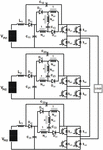
The block diagram of the proposed topology is shown in Figure 1. This work is organised as follows: In Section 2 the proposed topology is discussed. Section 3 describes design and implementation of GWO technique, Section 4 deals with simulation results and Section 5 gives brief discussion about experimental results. Finally, inferences are discussed in Section 6.
Figure 1 Block diagram of the proposed topology.
2 Description of the Proposed SCL qZS-CMI Topology
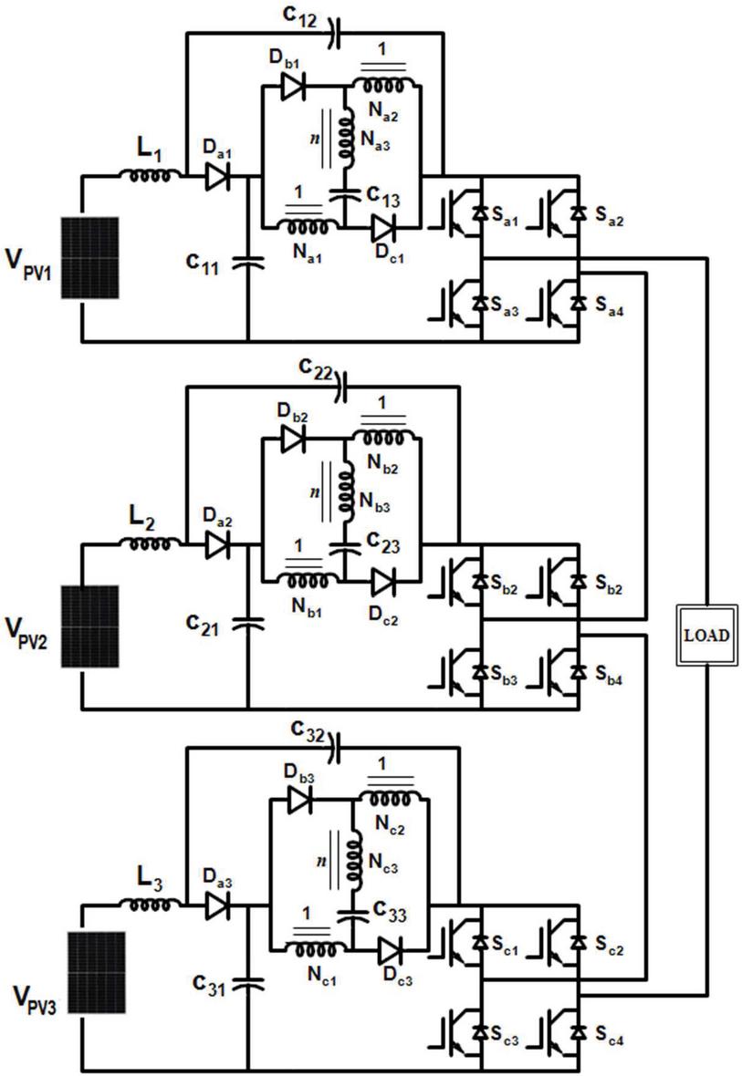
The three H-bridges of SCL qZS-CMI have similar capacitor values and inductor values. In each H-Bridge, a coupled inductor is connected with a pair of diodes (D, D), (D, D) and (D, D) as shown in Figure 2. The coupled inductor as the same number of turns N N turns ratio of winding is n N/N N/N.
Figure 2 Circuit diagram of SCL qZS-CMI with Solar PV system.
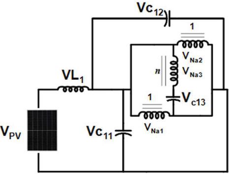
The turn’s ratio of windings is same for the other two H-bridges. SCL combines with one capacitor, two diodes in the existing model. It achieves high boost factor of 3/(1-4D) while comparing with traditional qZS-CMI. SCL has low stress on the components of the circuit. By comparing with the traditional qZS-CMI the size of the inductor is reduced. In shoot-through state diodes D, D, D will be OFF, whereas diodes (D, D), (D, D) and (D, D) will be ON. Windings (N, N), (N, N) and (N, N) are charged by parallel capacitors C, C, C, N, N and N produce energy to C, C, C and capacitors C, C, C will obtain energy. The leakage inductance is limited by charging current of capacitors C, C, C.
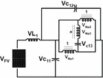
Figure 3 Shoot through operation of single of H-Bridge in SCL qZS-CMI.
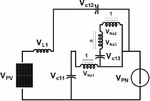
Figure 4 Non-shoot through operation of H-Bridge in SCL qZS-CMI a single Bridge in SCL qZS-CMI.
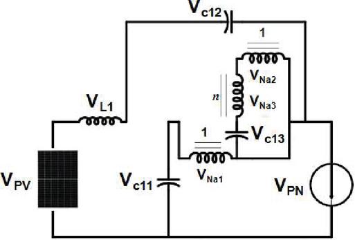
During non-shoot-through, it has six operating states and two non-operating states for SCL qZS-CMI. Diodes (D, D), (D, D) and (D, D) will be OFF, diodes D, D, D will be ON. The capacitors (C, C), (C, C) and (C, C) will be charged. The windings (N, N, N), (N, N, N) and (N, N, N) are in series with capacitors C, C, C to transfer energy to the main circuit. The leakage inductance of SCL qZS-CMI is absorbed by C, C, and C and they are recycled to avoid stress on switches. Figures 3 and 4 shows the shoot through and non-shoot through operation of the proposed circuit. By applying KVL to three H-Bridges during shoot through operation.
| (1) | ||
| (2) | ||
| (3) | ||
| (4) | ||
| (5) |
By applying KVL for three H-Bridges during non-shoot through operation;
| (6) | |
| (7) | |
| (8) |
In case of magnetic coupling, , the capacitor will be as a voltage source during non-shoot through state , , Hence Equations (7) and (8) of the first H-Bridge can be modified as,
| (9) | ||
| (10) |
SCL qZS-CMI is connected in series with individual PV sources. The switch count of the circuit is ‘4n’ where ‘n’ is number of PV sources. Three dc sources have the same voltage and the AC output voltage is attained by 2n+1 levels. The equation of SCL qZS-CMI with dc source is given as;
, where g 1, 2, 3,…,n. The voltage level of three H-Bridge of SCL qZS-CMI is generated as V, V V and V V V. Cascaded Multilevel Inverter operation is shown in Table 1. In Table 1, V V V V.
Table 1 Switching states of SCL qZS-CMI
| Voltage | 0 | V | 2V | 3V | 3V | 2V | V | 0 |
| Switch | ||||||||
| S | 1 | 1 | 1 | 1 | 0 | 0 | 0 | 0 |
| S | 1 | 0 | 0 | 0 | 1 | 1 | 1 | 0 |
| S | 0 | 0 | 0 | 0 | 1 | 1 | 1 | 1 |
| S | 0 | 1 | 1 | 1 | 0 | 0 | 0 | 1 |
| S | 1 | 1 | 1 | 1 | 0 | 0 | 0 | 0 |
| S | 1 | 1 | 0 | 0 | 1 | 1 | 0 | 0 |
| S | 0 | 0 | 0 | 0 | 1 | 1 | 1 | 1 |
| S | 0 | 0 | 1 | 0 | 0 | 0 | 1 | 1 |
| S | 1 | 1 | 1 | 1 | 0 | 0 | 0 | 0 |
| S | 1 | 1 | 1 | 0 | 1 | 0 | 0 | 0 |
| S | 0 | 0 | 0 | 0 | 1 | 1 | 1 | 1 |
| S | 0 | 0 | 0 | 1 | 0 | 1 | 1 | 1 |
3 Design of Grey Wolf Optimization (GWO)
GWO is one of the modern techniques applied for tracking in the PV system. It is developed based on consideration of iterations, where the traditional methods have only two possibilities in choosing the LP and the GP for achieving maximum power. The masters of the wolves are men and women, where they are known as alphas. The alphas are mainly taken into account for judging regarding hunting and other regular activities. The alphas judgements are informed to the group of wolves. Sometimes alphas follow other groups of the wolves depending upon the right behaviour. In meetings, the group will confess the alpha by handling their tail. The alpha wolves permit to amour in their group. The alpha controls the group that is the reason it is called as the strongest. The second type of wolves are called beta. This helps the alpha while taking decisions and it will also help other groups while taking decision. The beta wolf can be either men or women, the best wolf is alpha. Grey wolves have prey location recognizing ability and encircling them. In general, the hunt is guided by wolf, later beta and delta wolves join in the hunting process [24]. Moreover, it is divided into two types leader solutions and other solutions [25]. If one of the alpha wolf dies or becomes old the beta wolf gets the authorities and it should respect the alpha, but it is superior to other wolves. The beta is considered as a mentor for the alpha and the director for the wolves. The beta fulfils the alpha’s demand on the group and it gives a response to the alpha. The least level is omega. The omega will be the victim. The following equations are proposed for encircling the prey:
| (11) | |
| (12) |
Where t indicates the current iteration, F, E, G and B are coefficient vectors, Z is the position vector of the prey and Z indicates the position vector of the grey wolf.
The vectors G and E are calculated as follows;
| (13) | ||
| (14) |
where the elements of c are linearly decreased from 2 to 0 throughout iterations and l, l are random vectors in [0, 1]. Z is the position for finding the prey. Grey wolves can realize the location of prey and encircle them. In reference to derive the hunting behaviour of grey wolves, alpha gives the best solution, where beta and delta have better knowledge about finding the prey. The following equations are given:
| (15) | ||
| (16) | ||
| (17) |
Duty cycle D should be determined for algorithm, Hence, (11) is represented as:
| (18) |
Thus, the fitness function of the GWO algorithm is formulated as
| (19) |
Where P represents power, d is the duty cycle, i is the number of current grey wolves, and k is the number of iterations. In Figure 5 Flow chart of GWO is shown. The word ‘agent’ represents wolf in the flow chart.
Figure 5 Flow chart of GWO.
3.1 PV Panel Voltage Control to Achieve Maximum Power
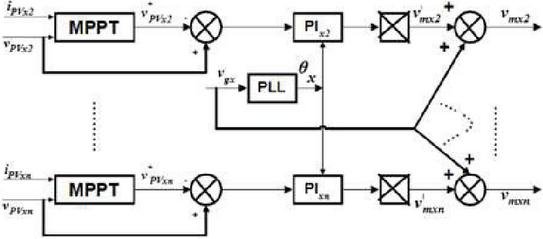
In Figure 6 PV panel voltage control is shown. By using PI regulators it is controlled to achieve maximum power for the SCL qZS-CMI modules from 2 to ‘n’ in phase, where for PIxn, n represents (n 2,3,…n). GWO is implemented because of its fast-tracking ability.
Figure 6 PV panel voltage control to achieve maximum power by MPPT.
3.2 PV Panel Voltage Control for All Modules in SCL qZS-CMI
Figure 7 shows the voltage control for all modules in PV panel. To enforce the sum of the PV panel voltage a PI regulator is employed in each phase
| (20) |
Figure 7 Voltage control of all modules in PV panel.
For tracking all the PV voltages
| (21) |
In Figure 6 the voltage is from the first module, from modules 2 to ‘n’ in MPPT is to . Through (21), the MPPT is achieved for SCL qZS-CMI.
4 Simulation Results
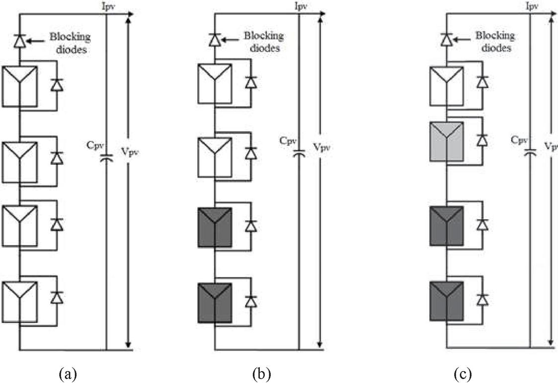
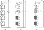
In this section performance based on without shading PV panels and with shading PV panels are shown in two different patterns, which are shown in Figure 8. Further results are shown by implementing traditional P & O method and GWO method.
Figure 8 (a) PV panel without PSC, (b) PV panel with PSC-Pattern 1, (c) PV panel with PSC- Pattern 2.
4.1 Simulation Investigation at Various PV Panel Irradiations
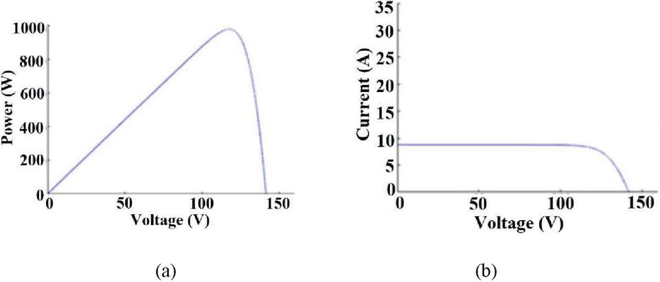
Figure 9(a) shows the power rating of 1000 W were voltage is 140 V and 8.5 A. In Figure 9(b) V-I characteristics is shown. As per datasheet, each PV panel is designed for 250 W and four 250 W panels are connected in parallel as shown in Figure 8(a).
Figure 9 (a) PV characteristics of PV panel without PSC, (b) VI characteristics of PV panel without PSC.
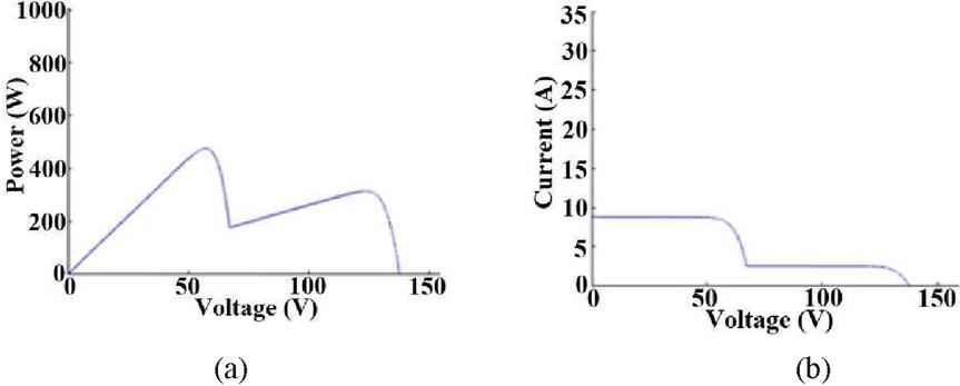
Figure 10 (a) PV characteristics of PV panel with PSC (Pattern 1), (b) VI characteristics of PV panel with PSC (Pattern 1).
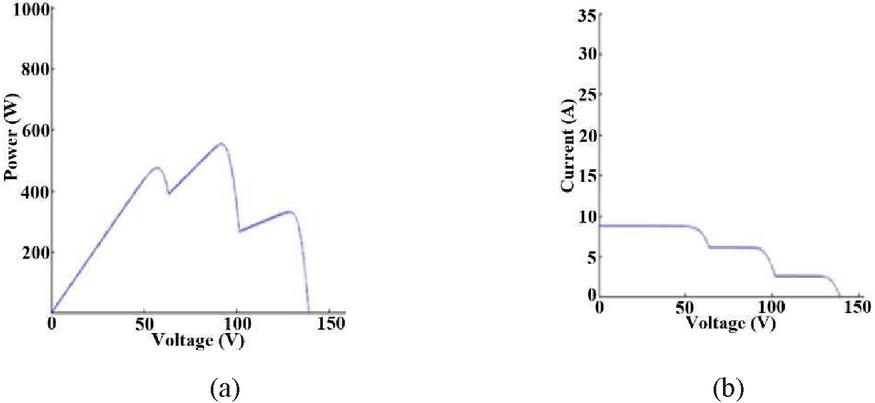
The PV characteristics with 2 panels irradiation of 500 W/m and the remaining 2 panels are configured with 1000 W/m irradiation as shown in Figure 8(b). Figure 10(a) represents PV characteristics and Figure 10(b) represents VI characteristics, where it has one local peak and one global peak. For the PSC which is shown in Figure 8(c), has three peaks, where two are local peaks and one is global peak as shown in Figures 11(a) and 11(b). The three irradiations are 1000 W/m, 700 W/m, and 500 W/m.
Figure 11 (a) PV characteristics of PV panel with PSC (Pattern 3), (b) VI characteristics of PV panel with PSC (Pattern 3).
Figures 12 and 13 shows the output power of P & O and GWO for without PSC. The output power has more distortions in the P & O technique due to the selection in maximum power. In GWO, the output power is very smooth where it chooses the maximum power with ease.
Figure 12 Simulation output power of P & O without PSC.
Figure 13 Simulation output power of GWO without PSC.
Figure 14 Simulation output power of P&O with PSC (Pattern 1).
Figure 15 Simulation output power of GWO with PSC (Pattern 1).
The output power of P & O and GWO under PSC for two peaks are shown in Figures 14 and 15 shadings are created as per Figure 8(b). In selecting the local peak and global peak for P & O, where the operation depends upon the before perturbation and the present perturbation of the duty cycle.
Figure 16 Simulation output power of P&O with PSC (Pattern 2).
Figure 17 Simulation output power of GWO with PSC (Pattern 2).
The output power for P & O and GWO under PSC for three peaks are shown in Figures 16 and 17, shadings are created as per Figure 8(c). In selecting the local peak and the global peak for P & O, it is critical where the operation depends upon the before perturbation and the present perturbation of the duty cycle. For three various irradiations, the output power may increase or decrease compared to two peaks. In GWO the output power is maximum, where it can operate under the given maximum iterations. Simulation parameters are tabulated in Table 2.
Table 2 Parameter values of the SCL qZS-CMI
| S.No | Parameter | Value |
| 1 | Inductors (L to L) | 560 H |
| 2 | Capacitors (C to C) | 470 F |
| 3 | Coupled Inductor (1:2:2) | 330 H |
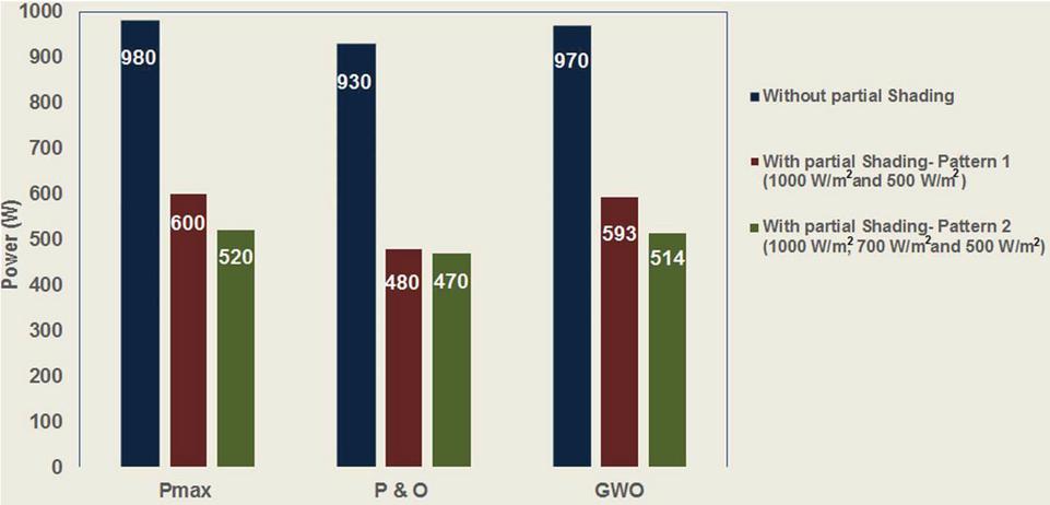
The efficiency is calculated by using (22). Figure 18 shows the simulation comparison graph for P & O and GWO without PSC and PSC. The graph represents maximum power attained without PSC and with PSC. GWO has higher efficiency and smooth output compared to P & O.
Figure 18 Simulation output power comparison without PSC and with PSC for P & O and GWO by implementing to SCL qZS-CMI.
5 Experimental Results
The experimental verification is performed for 1 Kw by building a bench set up. In Figure 19 the experimental setup of SCL qZS-CMI with a PV system is shown. The parameters chosen for the proposed SCL qZS-CMI are the same that have been implemented in simulation. The proposed system is built with TLP-350 optocoupler driver circuit. TheTLP-350 driver circuit is used for driving the pulses to the switches through connecting My-RIO pins. The power supply for driver circuit is given by using transformer 230/18V and it is stepped down to DC 15V which is enough for TLP-350.
Figure 19 Photograph of the experimental test bench of the SCL qZS-CMI with the PV system.
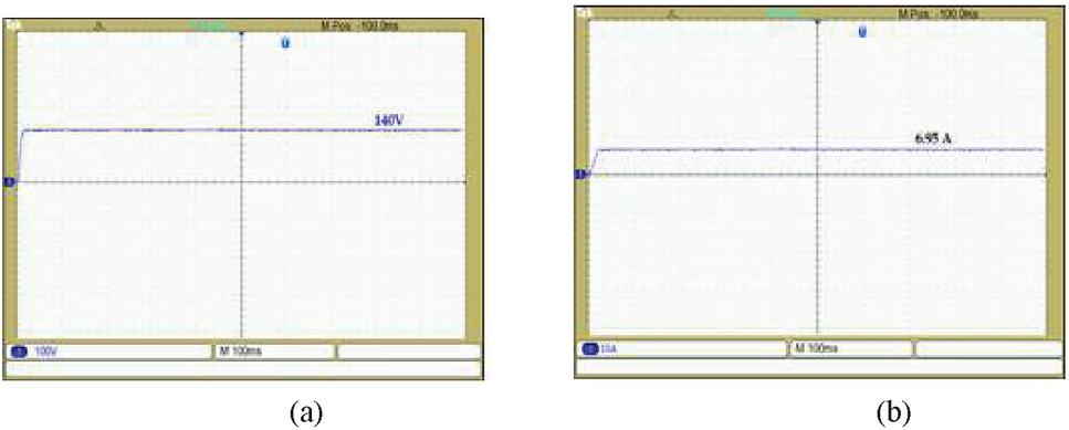
Figure 20 Experimental output voltage and output current of PV panel by using P&O (a) Output voltage (b) Output current.
Figure 21 Experimental output voltage and output current of PV panel by using GWO (a) Output voltage (b) Output current.
The experimental setup of the PV panel output voltage and the output current of P & O have been shown in Figure 20. Figure 20(a) represents the output voltage of 140 V and the output current of 6.64 A is shown in Figure 20(b). Figure 21 shows the output voltage and the output current of GWO. The output voltage is 140 V and 6.95 A. In the comparison of P & O and GWO, GWO has smooth output compared to P & O.
Different conditions were considered for experimental verification in a PV system for P & O and GWO. In Figure 22(a) the output power of SCL qZS-CMI with P&O technique is shown under uniform irradiation condition and Figure 22(b) is the output power of SCL qZS-CMI with GWO. In Figures 23(a) and (b), Figures 24(a) and (b) different partial conditions are considered.
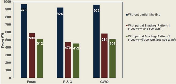
Figure 25 Experimental output power comparison without PSC and with PSC for P & O and GWO by implementing to SCL qZS-CMI.
In Figure 25 the output power for P & O and GWO is represented with PSC and without PSC. Clearly the graph defines GWO achieves maximum power with high efficiency compare to P & O under various conditions considerd for experimental verification.
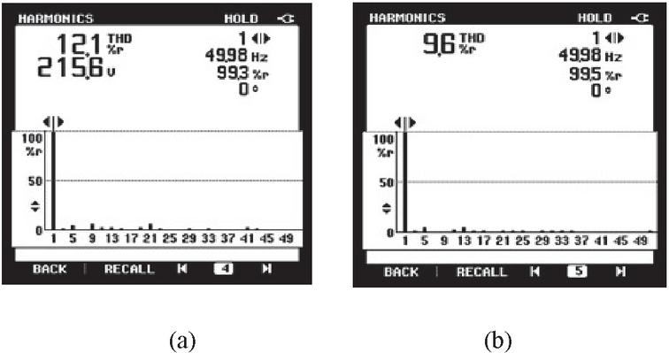
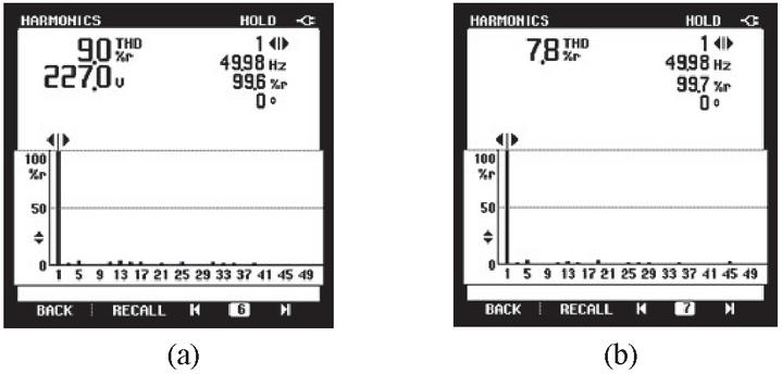
Figure 26 Experimental THD of P & O, (a) Output voltage THD of P& O (b) Output current THD of P&O.
Figure 27 Experimental THD of GWO, (a) Output voltage THD of GWO (b) Output current THD of GWO.
Figures 26 and 27 shows the experimental THD of P & O and GWO for output voltage and output current. The output voltage THD of P&O is found to be 12.1%, where the output voltage THD of GWO is 9.0%. In comparison with THD of output current, the output current THD of P & O is 9.6% and the output current THD of GWO is 7.8%. The THD is high for P&O while comparing to GWO. The reasons for high THD in P&O are due to distortions present in output power, where it can track only the previous perturbation and the present perturbation, whereas in GWO various iteration cycles can be tracked instantly for obtaining smooth output.
Conflict of Interest
There is no conflict of interest from the authors.
Conclusion
This work has discussed a comparative analysis by implementing P & O and GWO to the proposed SCL qZS-CMI topology. An experimental set up of seven-level SCL qZS-CMI is built. P & O and GWO algorithm results are analysed by utilizing four PV modules, which are configured under standard conditions. In addition, analysis is determined for PSC as well. The computer simulation is carried out for P & O and GWO technique for comparison. The whole setup is analysed based on maximum power tracking and THD. Simulation and experimental results are found to be similar. The analysis has proved that GWO has a better performance over P & O under both uniform and PSC of PV systems for the proposed PV fed SCL qZS-CMI topology.
References
[1] Zhang Z, Wang P (2020) Research on Synchronous Control Method for Suppressing Nonlinear Impulse Perturbation of Photovoltaic Grid-Connected Inverter. IEEE Access 8:43497–43507.
[2] Gupta KK, Ranjan A, Bhatnagar P, Sahu LK, Jain S (2016) Multilevel Inverter Topologies With Reduced Device Count: A Review. IEEE Transactions on Power Electronics 1:135–151.
[3] Panda RK, Mohapatra A, Srivastava SC (2019) Enhancing inertia of solar photovoltaic-based microgrid through notch filter-based PLL in SRF control. IET Generation, Transmission & Distribution 14:379–388.
[4] Nour AMM, Hatata AY, Helal AA, El-Saadawi M (2019) Review on voltage-violation mitigation techniques of distribution networks with distributed rooftop PV systems. IET Generation, Transmission & Distribution 14:349–361.
[5] Zeng J, Ning J, Du X, Kim T, Yang Z, Winstead V (2020) A Four-Port DC–DC Converter for a Standalone Wind and Solar Energy System. IEEE Transactions on Industry Applications 56:446–454.
[6] Rajvikram M (2019). The Motivation for Renewable Energy and its Comparison with Other Energy Sources: A Review. European Journal of Sustainable Development Research.
[7] Sangwongwanich A, Yang Y, Sera D, Blaabjerg F (2020) Mission Profile-Oriented Control for Reliability and Lifetime of Photovoltaic Inverters. IEEE Transactions on Industry Applications 56:601–610.
[8] Pashajavid E, Golkar MA (2013) Optimal placement and sizing of plug in electric vehicles charging stations within distribution networks with high penetration of photovoltaic panels. Journal of Renewable and Sustainable Energy 5:512–520.
[9] Gong Q, Midlam-Mohler S, Marano V, Rizzoni G (2012) Study of PEV charging on residential distribution transformer life. IEEE Trans. Smart Grid 3:404–412.
[10] Podder AK, Roy NK, Naruttam Kumar Roy, Pota HR (2019) MPPT methods for solar PV systems: a critical review based on tracking nature. IET Renewable Power Generation 13:1615–1632.
[11] Ishaque K, Salam Z, Shamsudin A, Amjad M (2012) A direct control based maximum power point tracking method for photovoltaic system under partial shading conditions using P & O algorithm. Appl. Energy 99:414–422.
[12] Chen K, Tian S, Cheng Y (2014) An improved MPPT controller for photovoltaic system under partial shading condition. IEEE Trans. Sustain. Energy 5:978–984.
[13] Kumar A, Gupta N, Gupta V (2019) Experimental prototype of a novel feed forward compensation for DC-link voltage stabilization in grid-tied PV system. International Transactions on Electrical Energy Systems 30:1–26.
[14] Bastidas-Rodriguez JD, Franco E, Petrone G, Ramos-Paja CA, Spagnuolo G (2014) Maximum power point tracking architectures for photovoltaic systems in mismatching conditions: a review. IET Power Electronics 7:1396–1413.
[15] Jana S, Kumar N, Mishra R, Sen D, Saha TK (2019) Development and implementation of modified MPPT algorithm for boost converter-based PV system under input and load deviation. International Transactions on Electrical Energy Systems 30:1–18.
[16] Husev O, Vinnikov D, Roncero-Clemente D, Chub A, Romero-Cadaval E (2021) Single-Phase String Solar qZS-based Inverter: Example of Multi-Objective Optimization Design. IEEE Transactions on Industry Applications 3: 3120–3130.
[17] Jiang LL, Maskell DL, Patra JC (2013) A novel ant colony optimization based maximum power tracking for photovoltaic systems under partially shaded conditions. Energy and Buildings 58:227–236.
[18] Liu L, Liu C, Gao H (2013) A novel improved particle swarm optimization maximum power point tracking control method for photovoltaic array by using current calculated predicted arithmetic under partially shaded conditions. Journal of Renewable and Sustainable Energy 5.
[19] Bingol O, Ozkaya B (2019) Analysis and comparison of different PV array configurations under partialvshading conditions. Solar Energy 160:336–343.
[20] Sridhar V, Umashankar S (2017) A comprehensive review on CHB MLI based PV inverter and feasibility study of CHB MLI based PV-STATCOM. Renewable and Sustainable Energy Reviews 78:138–156.
[21] Raghavendra Rajan V, Premalatha L (2017). Quasi-Z-Source Inverter Topologies with Reduced Device Rating: a Review. International Journal of Power Electronics and Drive System 8:325–334.
[22] Furqan Ahmed H, Cha H, Kim SH, Kim HG (2016) Switched-Coupled-Inductor quasi-Z-Source Inverter. IEEE Transactions on Power Electronics 31:1241–1254.
[23] Zhang M, Li H, Hao Y, Li K, Ding X (2021) A Modified Switched-Coupled-Inductor Quasi-Z-Source Inverter. IEEE Journal of Emerging and Selected Topics in Power Electronics 9: 3634–3646.
[24] Laxman B, Annamraju A, Srikanth NV (2021) A grey wolf optimized fuzzy logic based MPPT for shaded solar photovoltaic systems in microgrids. International Journal of Hydrogen Energy 46: 10653–10665.
[25] Meng K, Tang Q, Zhang Z, Yu C (2021) Solving multi-objective model of assembly line balancing considering preventive maintenance scenarios using heuristic and grey wolf optimizer algorithm. Engineering applications of artificial intelligence 1: 1–15.
Biographies

V. Raghavendra Rajan completed his Master’s Degree in Power Electronics and Drives at Jeppiaar Engineering College, Anna University, Chennai. Completed Ph.D. in Power Electronics with Renewable Energy from Vellore Institute of Technology, Chennai. His current research interest are Inverters, Embedded systems and Power Electronics for Renewable energy.

L. Premalatha did her Master’s at Thiagarajar College of engineering, Madurai, India, in 1997 and acquired her Ph.D., in Electrical Engineering from Anna University, India, in the year 2009. She is currently working as a Professor in Vellore Institute of Technology, Chennai, India. Her research interests include Power Electronics & Drives, Non-linear dynamic systems & control, Electromagnetic compatibility and Power quality.

Krismadinata was born in Padang Indonesia. He received the B.Eng. degree from Universitas Andalas, Padang, Indonesia, in 2000 and the M.Eng. degree from the Institute of Technology Bandung, Indonesia, in 2004 and the Ph.D. degree from the University of Malaya, Kuala Lumpur, Malaysia, in 2012. He is currently a Senior Lecturer with the Department of Electrical Engineering, Universitas Negeri Padang, where he is also the Director of Center for Energy and Power Electronics Research Universitas Negeri Padang. His research interests are power electronics, control system and renewable energy.
Distributed Generation & Alternative Energy Journal, Vol. 37_5, 1395–1416.
doi: 10.13052/dgaej2156-3306.3755
© 2022 River Publishers

