Dead-Time Effect and Compensation Technology for an Isolated Dual Active Bridge Converter
Xifeng Xie1,*, Deng Luo2, Jiangwei Wang1, Xuesong Wu1 and Tao Chen1
1Guangxi College of Water Resources and Electric Power, Nanning 530023, China
2School of Electrical Engineering, Southwest Jiaotong University, Chengdu 611756, China
E-mail: xiexifeng1027@yeah.net
*Corresponding Author
Received 04 November 2022; Accepted 01 December 2022; Publication 10 July 2023
Abstract
Aiming at deficiencies of output voltage distortion and circulating current generation caused by dead-time effect in the modulation process, a simple and feasible dead time compensation strategy is presented. Firstly, the influence of dead-time effect on the output voltage of bridge is analysed, and a dead time compensation strategy is added between the modulation signal and dead time procession. According to the current direction of the bridge, the rising edge or falling edge of the driving signal is selectively delayed to compensate for dead-time effect. Secondly, an Optimized Triple Phase-shift (OTPS) modulation strategy is adopted with minimizing leakage inductor current Root-Mean-Square (RMS) control, which minimizes current stress, achieves soft-switching operation, avoids phase-shift errors caused by Dead-Time Effect, and optimizes control performance of DC-DC converters. Finally, simulated and experimental results are added to verify the correctness and effectiveness of the proposed method.
Keywords: Dead-time effect, dead time compensation technology, dual active bridge converter, minimum current stress, triple phase-shift (TPS).
1 Introduction
With the fact of fossil energy exhaustion and global ecology environment deterioration, renewable energy generation has become one of the major development trends of the modern power systems. Therefore, the key equipment of renewable energy systems has also become research hotspot [1–5]. As one of the key energy conversion components, high-power dc–dc converters play an important role in dc distribution systems and energy storage systems [6–9]. The dual active bridge (DAB) is a widely known topology for high-power dc–dc conversions with bidirectional power-transfer capability, high power density and zero voltage switching (ZVS) capability [10–13]. Dead time between the complementary driving signals is needed to avoid short circuit in DAB converter, however, dead-time effect of the modulation process leads to output voltage distortion and circulating current generation, which has become an apparent issue in high-switching-frequency high-power DAB DC-DC converter [14–17].
Recently, many researches have tried to resolve the above problem. In [18], segment-dividing model of Phase-shifted full-bridge converter is proposed and dead time expression is optimized, which broadens soft-switching range. In [19], dead time optimization expression is proposed, however, it does not consider minimizing the leakage inductor current RMS. In [20], the optimal dead time is determined by a large number of experiments in a specific converter, but theoretical analysis is not provided for specific optimization methods. In [21], a simple dead time compensation method is proposed, which requires additional hardware circuits to detect conducting time of the converter transistor, as a result, the hardware circuit complexity of the converter is increased. In order to save hardware costs, a dead time compensation strategy based on voltage space vectors is proposed, but it is incompatible with other modulation methods [22]. Additionally, in [23], a dead time compensation strategy based on volt-time equivalent principle is proposed, and the complexity of the control system can be decreased. In [24], the loss in dead time is analysed in detail, the switching losses can be reduced, and the system efficiency can be improved. In [25], a multi-objective optimization method of leakage inductor current and ZVS range is presented. In [26], peak current is selected as the target under TPS control to achieve low conduction loss, which simplifies calculation and optimizes process. Unfortunately, all the above-mentioned modulation schemes fail to consider the existence of dead time, which seriously affects the safe operation of DAB.
According to the current direction of the bridge, a dead time compensation strategy for the modulation signal is proposed, which is based on the influence of dead-time effect on the output voltage of DAB converter. Furthermore, an Optimized Triple Phase-shift strategy is adopted, to make DAB converter operate under the minimum current stress, and the control curve of minimizing leakage inductor current RMS control is derived in detail, which is based on leakage inductor current RMS and zero voltage switching (ZVS). According to the curve, transformer secondary side duty-cycle is controlled to realize minimizing leakage inductor current RMS and soft-switching, which avoids phase-shift errors caused by Dead-Time Effect. the minimum current stress and soft-switching operation can be guaranteed, and the transfer efficiency of DAB converter can be improved. Finally, the simulation model as shown in Figure 1 is established in the MATLAB/Simulink, the experiment platform is built, and the proposed dead time compensation strategy is verified by simulation and experiment.
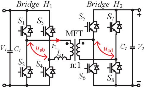
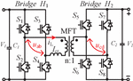
Figure 1 Topology of bidirectional isolated DAB converter.
2 Dead Time Mechanism and Dead Time Effect
2.1 Dead Time Mechanism
The topology of bidirectional isolated DAB converter is depicted in Figure 1, which is constructed by two full bridges and a high-frequency isolated transformer with the turns ratio n:1. and denote separately input voltage and output voltage of DAB converter, MFT denotes intermediate frequency isolation transformer, and are ac output voltages of two bridges H and H, respectively denote leakage inductance of the transformer, denote the current of , and denote the switching cycle. On/off states of the switching devices and , and , and , and are complementary. In order to avoid that and are directly applied to a single switch device, which will cause a short-circuit between the complementary driving signals, to avoid shoot-through phenomenon and guarantee the reliability of the converter, dead time is necessary to be inserted between the interlocked switches in the same bridge. There are two sequences in the three-level drive circuit of H-bridge structure, taking the primary side three-level as an example, there are (defined as “mode 1”) and (defined as “mode 2”). Take mode 1 as an example, when turns off, will not turn on immediately due to the existence of dead-time effect.
2.2 Dead Time Effect
To simplify the following derivation, some assumptions are made as follows: Dead time is defined as , when power is transmitted from ab side to cd side, it is defined as forward power transfer. Transformation ratio of controller is , conversion ratio between the actual input and output voltage is , primary side duty ratio is defined as , and secondary side duty ratio is defined as . Taking primary H-bridge structure (mode 1) as an example, the influence of dead-time effect on the bridge voltage is analysed.
Under the conditions of and , , the waveform of the transformer current is shown in Figure 2.
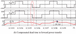
During forward power transfer, the rising edge of the positive half-cycle of is taken as the initiation point of a current cycle (align edge of and ). When the initial current is negative, dead-time effect has no effect on , and the phase of is delayed for one because of dead-time effect, as shown in Figure 2(a) “ uncompensated ”. When the initial current is positive, dead-time effect has no effect on , and the pulse width of is decreased by one , as shown in Figure 2(a) “ uncompensated ”. As a result, the transformer current is advanced to cross zero, circulating current is found on the secondary side of transformer, and DC offset is generated by transformer current.
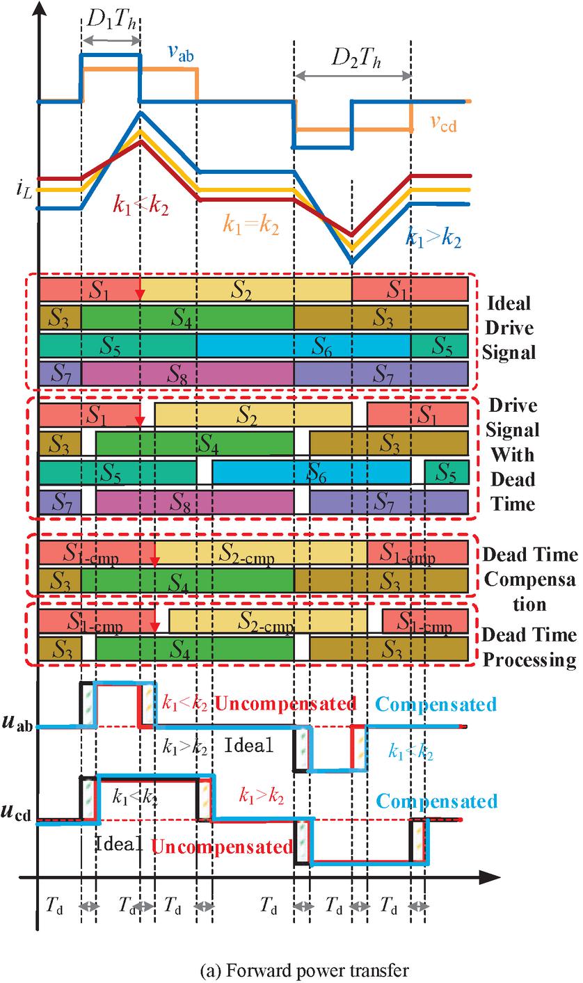
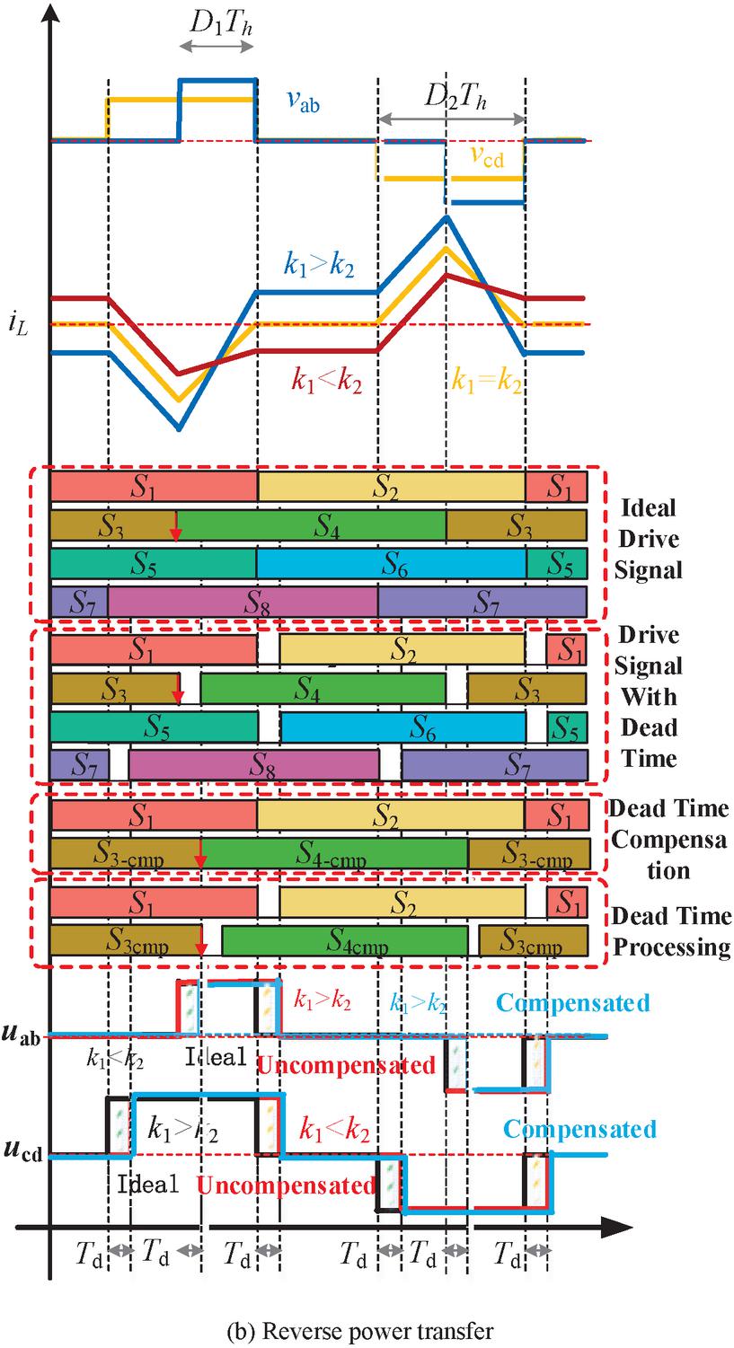
Figure 2 The influence and compensation of dead-time effect.
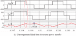
During reverse power transfer, the falling edge of the positive half-cycle of is taken as the initiation point of a current cycle(align edge of and ). When the initial current is negative, dead-time effect has no effect on , and the pulse width of is increased one because of dead-time effect, as shown in Figure 2(b) “ uncompensated ”, as a result, the transformer current is delayed to cross zero. When the initial current is positive, dead-time effect has no effect on , and the phase of the is delayed for one , as shown in Figure 2(b) “ uncompensated ”.
Based on the above analysis, output voltage distortion and circulating current generation are caused by dead-time effect in the modulation process. Therefore, it is necessary to compensate for dead-time effect. The specific impact of dead-time effect on the bridge voltage is as summarized in Table 1, the influence of dead-time effect on the bridge voltage of the primary side is the pulse width, and the influence on the bridge voltage level of the secondary side is the phase.
Table 1 The influence of dead-time effect on bridge voltage
| Power | |||
| Transfer | Initial Current | The Influence of Dead-time Effect | |
| Direction | Direction | ||
| Forward | Positive () | Pulse width decrease: one | No influence |
| Negative () | No influence | Phase lag: one | |
| Reverse | Positive () | No influence | Phase lag: one |
| Negative () | Pulse width Increase: one | No influence | |
2.3 Dead Time Compensation Strategy
From the above analysis, it can be found that there are three types of influence of dead-time effect on the bridge voltage: phase lagging, pulse width increasing and pulse width decreasing.
During forward power transfer, when the initial current is positive (), the pulse width of is decreased by , as shown in Figure 2(a). Therefore, it is necessary to increase one pulse width that is, the falling edge of the driving signal of the switching device is delayed for one , as shown in Figure 2(a)” Dead Time Compensation and ”
During reverse power transfer, When the initial current is negative (), the pulse width of is increased by one , as shown in Figure 2(a). Therefore, it is necessary to increase one pulse width, that is, the falling edge of the driving signal of the switching device is delayed one , as shown in Figure 2(b) “Dead Time Compensation and ”.
Comparing compensated bridge voltage level with ideal bridge voltage level, the pulse width of each voltage level is the same, however, compensated bridge voltage level lags behind ideal bridge voltage level by one in phase, and the phase lag can be compensated by phase delay.
3 Modulation Methods
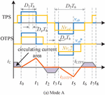
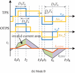
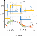
In order to improve the system efficiency by reducing switching loss and conduction loss simultaneously, an Optimized TPS modulation method is proposed. Figure 3 depicts the typical operating waveforms of DAB converter under TPS control and OTPS control, respectively.
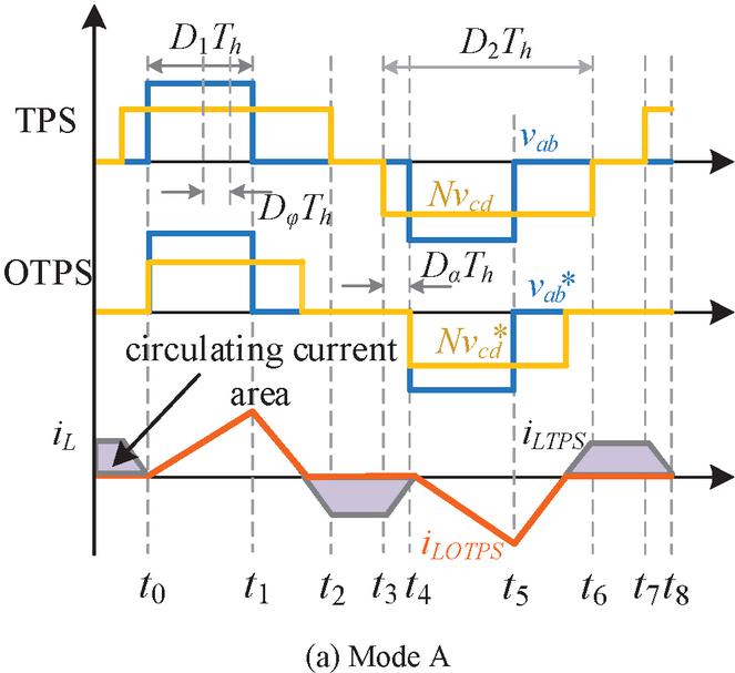
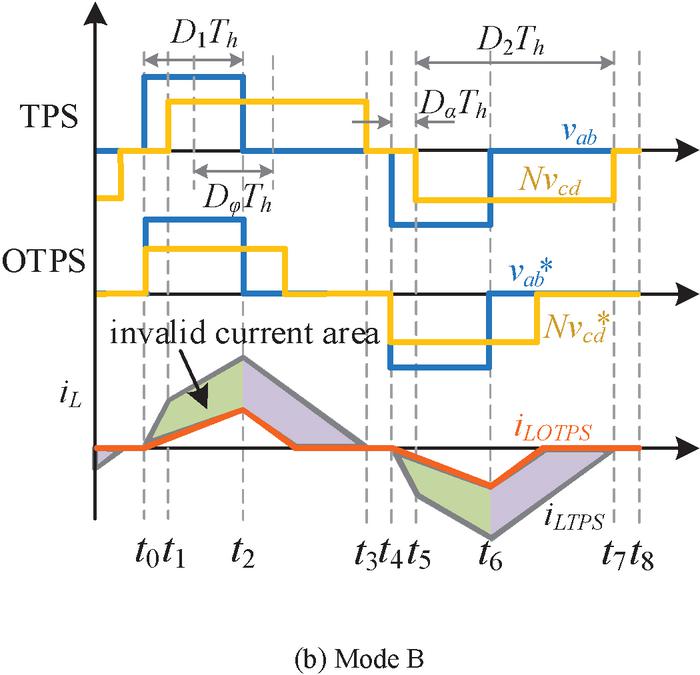
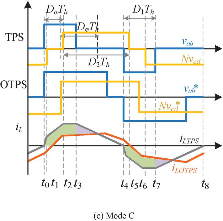
Figure 3 Operating waveforms of DAB under the TPS and OTPS.
3.1 TPS Modulation
The phase-shift angle between the positive level midpoint of and is defined as .
| (1) |
Based on the rising edge of from 0 to /2, as the rising edge of from 0 to /2 moves backward, is Slowly increases. There are three main operating modes of the circuit: mode A, mode B and mode C.
3.2 OTPS Modulation
As shown in Figure 3, DAB under TPS modulation strategy has problems such as large leakage inductance current stress and circulating current. In order to further reduce the current stress, improve the dynamic response performance, and eliminate circulating current and realize ZVS soft-switching of all switches over a wide operation range, it is necessary to optimize TPS modulation strategy. The optimized modulation parameters , and are selected to further reduce leakage inductor current RMS under the condition ZVS. In addition, leakage inductor current RMS is reduced to zero at no-load.
(1) Mode A The expression of leakage inductor current RMS in mode A is ). In the formula, and are respectively solved to make the two partial derivatives zero, and and that minimize leakage inductor current RMS are obtained.
| (2) |
The operating waveform of OPTS in mode A is as shown in Figure 3(a).
(2) Mode B The expression of leakage inductor current RMS in mode B is ), is solved to make the partial derivative zero and is arrived.
| (3) |
The operating waveform of OPTS in mode B is as shown in Figure 3(b).
(3) Mode C The expression of leakage inductor current RMS in mode C is ). In the formula, and are respectively solved to make the two partial derivatives zero, and and that minimize leakage inductor current RMS are obtained.
| (4) |
Where, , phase-shift duty-cycle dividing points and are expressed as:
| (5) |
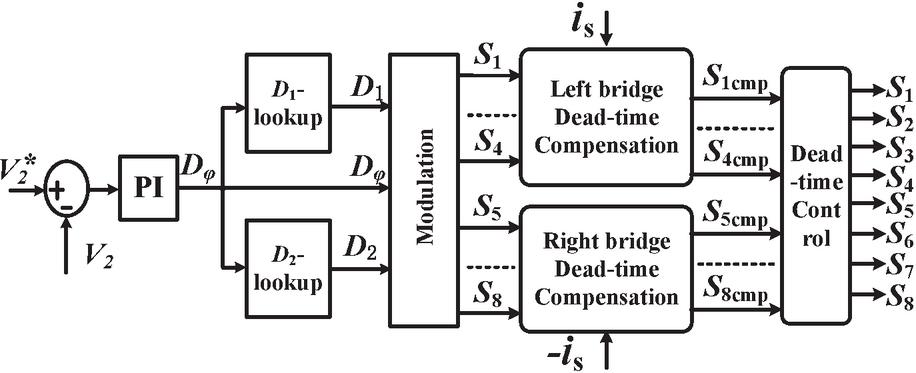
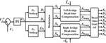
Figure 4 Control block diagram of DC-DC converter.
The operating waveform of OPTS in mode C is as shown in Figure 3(c).
Figure 4 shows control block diagram of DC-DC converter. A difference value () is obtained by comparing the actual value with the reference value , and phase-shift ratio is regulated by PI controller, then and are obtained by Equations (2), (4), (5) and (6), respectively, , and are input to the modulation module, and drive signals S–S are obtained through modulation operation, dead time of the driving signals S–S is used to process in dead time compensation module. According to the direction of the bridge current, the rising edge or falling edge of the driving signal is selected to reasonably compensate dead time, the compensation signal is output to dead time processing module to obtain the driving signals S–S of the switches.
4 Experimental Verification
4.1 Simulation Verification
The simulation model of bidirectional isolated three-level DC-DC converter shown in Figure 1 is established in MATLAB/Simulink, and the simulation parameters are listed in Table 2.
Figure 5 illustrates the simulation results of dead time compensation.
Table 2 The parameter of dead time compensation simulation
| Simulation Parameters | Value |
| Rated Power | 250 kW |
| Input DC Voltage | 800 V |
| Inverter Output Voltage RMS | 120 V |
| DC Capacitor | 4000 F |
| Switching Frequency | 10 kHz |
| Dead Time | 2 s |
| Leakage inductance | 4 H |
| Leakage inductor resistance | 8.8 m |
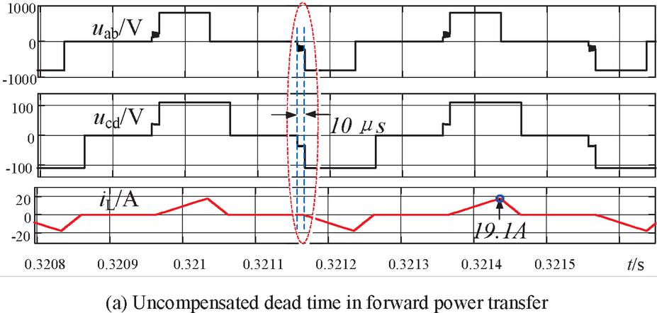
Figure 5 Continued
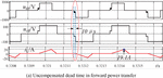
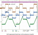
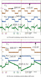
Figure 5(a) gives the simulation results of voltage , voltage and current , when dead time is not compensated in forward power transfer.
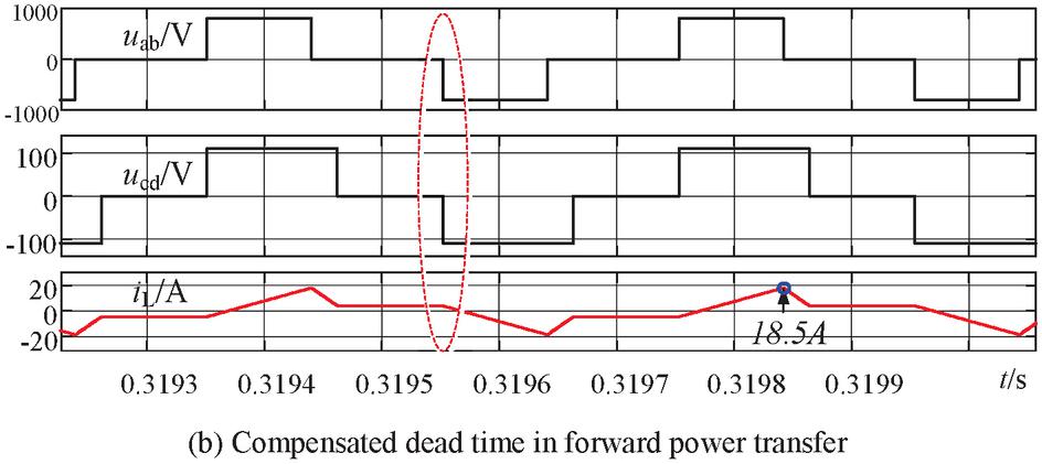
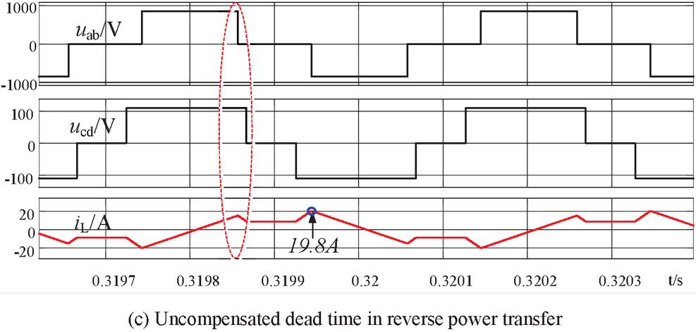
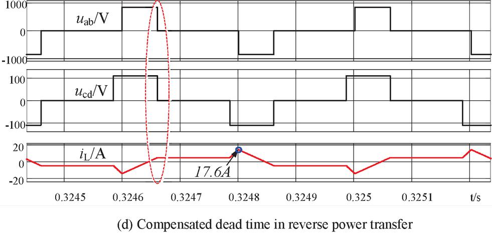
Figure 5 The simulation results of dead time compensation.
Figure 5(b) gives the simulation results of voltage , voltage and current , when dead time is compensated in forward power transfer.
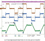
Figure 5(c) gives the simulation results of voltage , voltage and current , when dead time is not compensated in reverse power transfer.
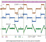
Figure 5(d) gives the simulation results of voltage , voltage and current , when dead time is compensated in reverse power transfer.
By comparing the waveforms of voltage , voltage and current in the case of dead time compensation in forward power transfer and reverse power transfer, the conclusions are as followed. When dead time is not compensated, the waveforms of voltage and voltage are not square waves, voltage sag and duty-cycle abnormality occur in dead time, phase relationship between voltage and current is changed, and the zero-crossing point of transformer current is not at the time when the polarity of H-bridge output level changes, duty-cycle is lost by 10s in forward power transfer. After dead time is compensated, there is no loss of duty-cycle. In forward power transfer, leakage inductance current is decreased from 19.1A to 18.5A, a decrease of 3.14 per cent. In reverse power transfer, leakage inductance current is decreased from 19.8A to 17.6A, a decrease of 3.14 per cent. The waveforms of voltage and voltage are square waves. There is no voltage offset in dead time. Zero-crossing point of the transformer current happens at the time when the polarity of H-bridge output level changes, therefore, period decoupling of adjacent switching is ensured, and good soft-switching performance can be achieved, so that the accurate control of the average current transmitted at the AC side can be realized, and current distortion at the grid side can be suppressed; at the same time, circulating current is eliminated, which contributes to the improvement of system efficiency. The simulation results verify that the proposed control strategy is correct and effective.
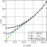
In order to verify the effect of OTPS modulation strategy on improving system efficiency, The curves of leakage inductor current RMS with respect to transmission power under OTPS, TPS and phase-shift control are compared in Figure 6. The transmission power of the converter changes from no-load to full load. Leakage inductor current RMS in no-load condition is about 48A and 80A under TPS and phase-shift control, under OTPS control, leakage inductor current RMS in no-load condition is close to 0, and leakage inductor current RMS under light-load operation is the smallest. The simulation results are consistent with theoretical analysis, which shows that OTPS modulation strategy effectively improves the system efficiency by eliminating circulating current and optimizing transformer current RMS.
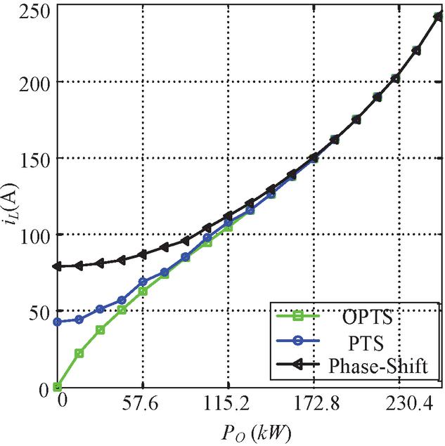
Figure 6 Comparison curve of leakage inductor current RMS under OTPS, TPS and phase-shift control.
4.2 Experimentational Verification
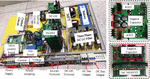
In order to further verify the correctness and effectiveness of the proposed dead time compensation strategy, Prototype photograph of the DAB system shown in Figure 7 is built according to DC-DC converter shown in Figure 1. FPGA chip EP3C55F484I7 was selected as the main controller, Verilog is used to design the proposed dead time compensation strategy. The parameters of the experimental system are listed in Table 3.
Table 3 Main Parameters of dead time compensation experiment
| Experimental Parameters | Value |
| Input DC Voltage | 120 V |
| Inverter Output Voltage RMS | 20 V |
| Switching Frequency | 10 kHz |
| Dead Time | 2 s |
| Auxiliary Inductance | 1.5 mH |
| DC Capacitor | 100 F |
| Input side MOSFETs | PT015N10N5 |
| Output side MOSFETs | C3M0065090J |
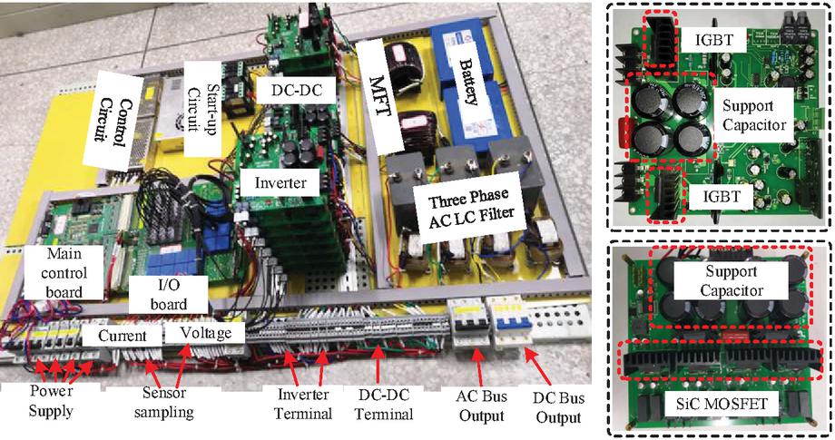
Figure 7 Prototype photograph of the DAB system.
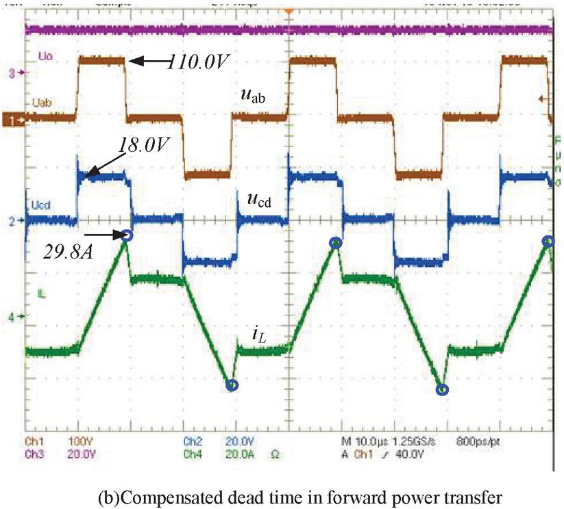

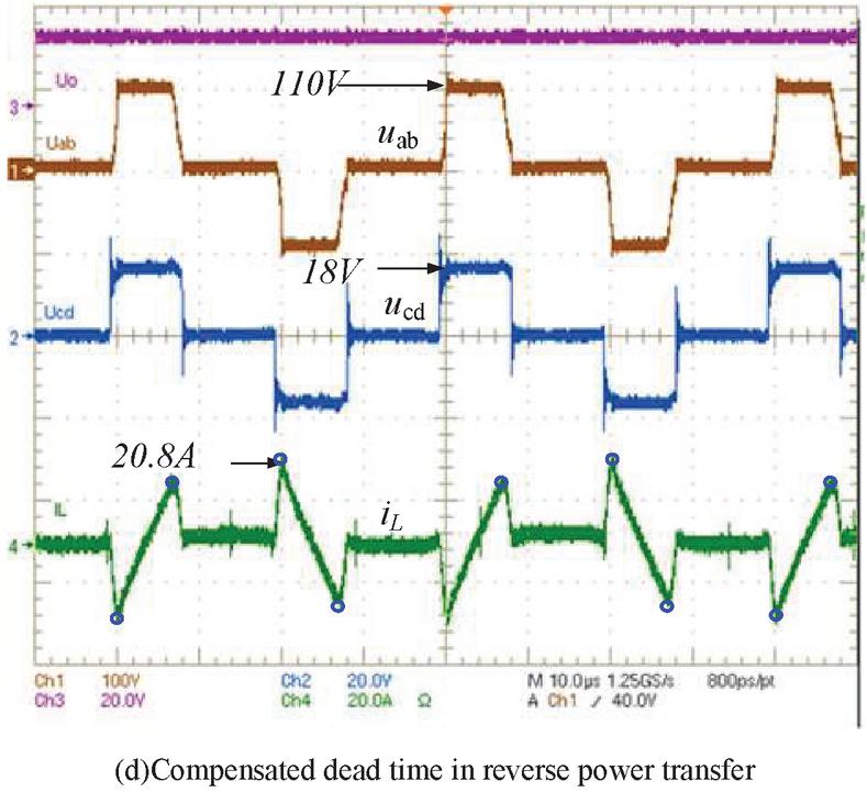
Figure 8 The experimental results of dead time compensation.
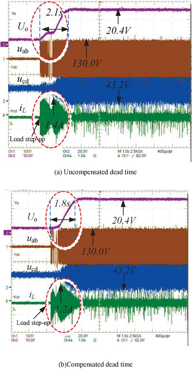
Figure 9 Startup experiment.
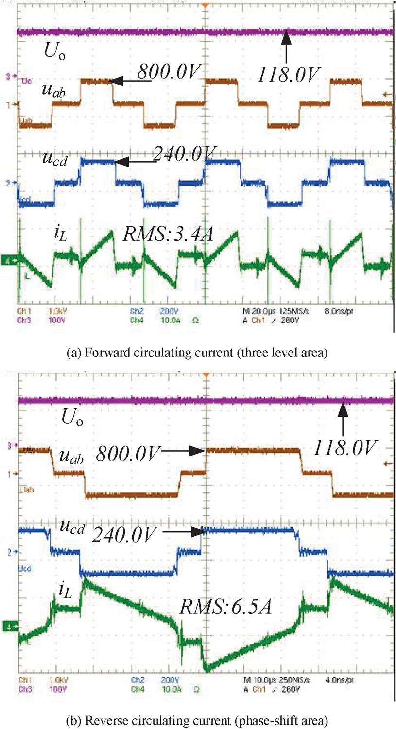
Figure 10 Stability of dead time compensation in circulating current.
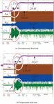
The static experimental results of dead time compensation are shown in Figure 8. Figures 8(a) and 8(b) demonstrate the experimental results of voltage , voltage , voltage and current under uncompensated dead time and compensated dead time in forward power transfer respectively. Figures 8(c) and 8(d) demonstrate the experimental results of voltage , voltage , voltage and current under uncompensated dead time and compensated dead time in reverse power transfer respectively. The output voltage is distorted under uncompensated dead time, the output voltage is a complete square wave under compensated dead time, and ZVS soft-switching of all switches over a wide operation range are realized. In forward power transfer, leakage inductance current is decreased from 36.5A to 29.8A, a decrease of 18.56 per cent. In reverse power transfer, leakage inductance current is decreased from 24.7 to 20.8A, a decrease of 15.79 per cent.
Figure 9 presents the results of the start-up experiment with and V. Figure 9(a) shows that output voltage shakes during startup under uncompensated dead time, and the voltage fluctuates during operation. leakage inductance current increases by about 1.4A, and DC voltage stably outputs 20.4V for about 2.1s; Figure 9(b) shows that output voltage is always stable during startup under compensated dead time, and voltage and current do not fluctuate during operation. leakage inductance current increases by about 1.2A, and DC voltage stably outputs 20.4V for about 1.8s, which achieve a smoother dynamic waveform and a faster dynamic response.
Figure 10 illustrates stability of dead time compensation in forward circulating current. The compensation deviation threshold is 1%, and circulating current is eliminated, which improves the system efficiency and ensures the decoupling of the transformer currents in adjacent switching periods, as a result, the accurate control of the AC side transmission current is realized, and current distortion is suppressed. The experimental results show that the proposed dead time compensation technology and OTPS modulation strategy are effective and feasible.
5 Conclusion
Aiming at the problem that dead time in the modulation process leads to output voltage distortion and circulating current generation, a dead time compensation strategy is proposed. An optimized TPS modulation strategy based on minimizing leakage inductor current RMS control is adopted. According to the expression of transformer leakage inductance current RMS and ZVS condition, control curve of minimizing leakage inductor current RMS control is derived. according to the control curve, the duty ratio of high-voltage side of the converter is controlled to minimize transformer leakage inductance current RMS, ensuring ZVS for switches and reducing the current stress over wide power and voltage ranges. The proposed dead time compensation strategies are verified by MATLAB simulations and experimental results on a downscaled DAB system.
Acknowledgment
This work was supported by the High level Innovation Team and Distinguished Scholar Program of Guangxi Higher Education institutions (Grant Guangxi teach talent [2020] No.6) and Sichuan Provincial Regional Innovation Cooperation Project (Grant No. 2021YFQ0051).
References
[1] Zhao Nannan, Zhou Feng, Ding Dawei, et al. Suppression strategy of grid-side current harmonics for electrolytic capacitor-less permanent magnet motor drives[J/OL]. Proceedings of the CSEE, 2022, 42(3):1145–1153 (in Chinese).
[2] Xiao Hongwei, He Yingjie, Liu Jinjun, et al. Research on vector asymmetric dead-time compensation modulation strategy of three-level inverter based on narrow pulse elimination [J]. Proceedings of the CSEE, 2021, 41(4):1386–1397 (in Chinese).
[3] Ding Xiaofeng, Zhou Yang, Cheng Jiawei. A review of gallium nitride power device and its applications in motor drive[J]. CES Transactions on Electrical Machines and Systems, 2019, 3(1):54–64.
[4] Huang Qingyun, Yu Ruiyang, Ma Qingxuan, et al. Predictive ZVS control with improved ZVS time margin and limited variable frequency range for a 99% efficient, 130-W/in3 MHz GaN totem-pole PFC rectifier [J]. IEEE Transactions on Power Electronics, 2019, 34(7): 7079–7091.
[5] Wang Yifeng, Chen Bo, Hou Yuqi, et al. Analysis and design of a 1-MHz bidirectional multi-CLLC resonant DC-DC converter with GaN devices[J]. IEEE transactions on Industrial Electronics, 2020, 67(2):1425–1434.
[6] Qin Haihong, Peng Zihe, Zhang Ying, et al. A comparative study of freewheeling methods for eGaN HEMTs in a phase-leg configuration[J]. IEEE Journal of Emerging and Selected Topics in Power Electronics, 2021, 9(3):3657–3670.
[7] Samajdar D, Bhattacharya T, Dey S. A reduced switching frequency sorting algorithm for modular multilevel converter with circulating current suppression feature[J]. IEEE Transactions on Power Electronics, 2019, 34(11):10480–10491.
[8] Zhang Yi, Chen Cai, Xie Yue, et al. A high-efficiency dynamic inverter dead-time adjustment method based on an improved GaN HEMTs switching model[J]. IEEE Transactions on Power Electronics, 2022, 37(3):2667–2683.
[9] Zhang Lei, Yuan Xibo, Zhang Jiahang, et al. Modeling and implementation of optimal asymmetric variable dead-time setting for SiC MOSFET-based three-phase two-level inverters [J]. IEEE Transactions on Power Electronics, 2019, 34(12):11645–11660.
[10] Yang Guanghui, Yang Jiaqiang, Li Sheng, et al. Overmodulation strategy for seven-phase induction motors with optimum harmonic voltage injection based on sequential optimization scheme[J]. IEEE Transactions on Power Electronics, 2021, 36(12):14039–14050.
[11] Wang Mingda, Zhang Xing, Zhao Tao, et al. An optimized third harmonic compensation strategy for single-phase cascaded h-bridge inverter[J]. Proceedings of the CSEE, 2020, 40(4):1073–1081 (in Chinese).
[12] C. Shen, H. Wu, “A Three-Phase Asymmetrical Dual-Active-Bridge Converter With Series/Parallel-Reconfigurable Output for Wide Voltage Range Applications” in IEEE Transactions on Industrial Electronics, vol. 68, no. 9, pp. 7714–7724, Sep. 2021.
[13] J. Duan, D. Zhang, L. Wang, “Active Voltage Sharing Module for Input-Series Connected Modular DC/DC Converters” in IEEE transactions on Power Electronics, Vol. 35, no. 6, pp. 5987–6000, Jun. 2020.
[14] F. An, W. Song, K. Yang, S. Yang, and L. Ma, “A simple power estimation with triple phase-shift control for the output parallel DAB DC–DC converters in power electronic traction transformer for railway locomotive application,” IEEE Trans. Transp. Electrif., vol. 5, no. 1, pp. 299–310, Mar. 2019.
[15] Y. D. Xiao, Z. Zhang, M. A. E. Andersen, and B. E. Thomsen, “Partial parallel dual active bridge converter with variable voltage gain for SOEC/SOFC system,” in Proc. IEEE Appl. Power Electron. Conf. Expo., 2019, pp. 1641–1646.
[16] N. Hou, W. Song, Y. Li, Y. Zhu, and Y. Zhu, “A comprehensive optimization control of dual-active-bridge DC–DC converters based on unified phase-shift and power-balancing scheme,” IEEE Trans. Power Electron, vol. 34, no. 1, pp. 826–839, Jan. 2019.
[17] Yan, Y., Gui, H., Bai, H. Complete ZVS Analysis in dual-active-bridge. IEEE Trans. Power Electron. 2020, 36, 1247–1252.
[18] Teng J H, Liu Binhan. Three-stage dead-time adjustment scheme for conversion efficiency enhancement of phase-shift full-bridge converters at light loads[J]. IEEE Transactions on Industrial Electronics, 2021, 68(2):1210–1219.
[19] Tebianian H, Salami Y, Jeyasurya B, et al. A 13.56-MHz full-bridge class-D ZVS inverter with dynamic dead-time control for wireless power transfer systems[J]. IEEE Transactions on Industrial Electronics, 2020, 67(2):1487–1497.
[20] Mu Kun, Li Yundi and He Guofeng, Balancing control of capacitance voltage for modular multilevel converter based on carrier phase shifted technique[J]. Renewable Energy Resources, 2020, 38(10):1389–1393.
[21] Moon S, Chen C, Wang R J. A new dead time regulation synchronous rectification control method for high efficiency LLC resonant converters[J]. IEEE Transactions on Power Electronics, 2021, 36(9):10673–10683.
[22] Asad M, Singha A K, Rao R M S. Dead time optimization in a GaN-based buck converter[J]. IEEE Transactions on Power Electronics, 2022, 37(3):2830–2844.
[23] Chiu P K, Wang Pinying, Li Shengteng, et al. A GaN driver IC with novel highly digitally adaptive dead-time control for synchronous rectifier buck converter [C]//Proceedings of 2020 IEEE Energy Conversion Congress and Exposition. Detroit: IEEE, 2020:3788–3792.
[24] Sarkar A, Vankayalapati B T, Anand S. GaN-based multiple output flyback converter with independently controlled outputs[J]. IEEE Transactions on Industrial Electronics, 2022, 69(3):2565–2576.
[25] P. Liu, C. Chen, and S. Duan, “An optimized modulation strategy for the three-level DAB converter with five control degrees of freedom,” IEEE Trans. Ind. Electron., vol. 67, no. 1, pp. 254–264, Jan. 2020.
[26] W. Zhao, X. Zhang, S. Gao, and M. Ma, “Improved model-based phaseshift control for fast dynamic response of dual-active-bridge DC/DC converters,” IEEE J. Emerg. Sel. Topics Power Electron., vol. 9, no. 1, pp. 223–231, Feb. 2021.
Biographies

Xifeng Xie received the B.S. and M.S. degrees in electrical engineering from Southwest Jiaotong University, Chengdu, China, in 2002 and 2006. He has worked in Guangxi Vocational College of Water Resources and Electric Power since 2006, and has been a Professor, since 2019. His research interests include bidirectional power conversion, smart micro-grid, and grid integration of renewable energy.

Deng Luo received the B.S. and M.S. degrees in electrical engineering from Southwest Jiaotong University, Chengdu, China, in 2015 and 2018. He is currently working as an product manager at the Chengdu Yunda Technology Co., Ltd. His research field mainly covers the electric transmission system of EMU and traction transmission system of urban rail electric train.

Jiangwei Wang received the B.S. degrees in Control Technology and Instrument from Harbin Institute of Technology, Harbin, China, in 2010, he received the M.S. in Electrical Engineering and Automation from Guangxi University, Nanning, China, in 2016. he has worked in Guangxi Vocational College of Water Resources and Electric Power since 2016, and has been a lecturer, since 2019. His research interests include new energy power generation, micro grid and power storage system.

Xuesong Wu received the B.S. degrees in Agricultural Electrification and Automation from Hebei Agricultural University, Baoding, China, in 2001, he received the M.S. in Agricultural Electrification and Automation from Guangxi University, Nanning, China, in 2004. he has worked in Guangxi Vocational College of Water Resources and Electric Power since 2017, and has been a senior engineer, since 2010. His research interests include PET, smart micro-grid, and grid integration of renewable energy.

Tao Chen received the B.S. degrees in Electrical Engineering and Automation from Harbin University of Science and Technology, Harbin, China, in 2003, he has worked in Guangxi Vocational College of Water Resources and Electric Power since 2018, and has been a senior engineer, since 2016. His research interests include modelling and control of power electronics converters, high-efficiency power conversion, and magnetic integration in power converters.
Distributed Generation & Alternative Energy Journal, Vol. 38_5, 1357–1382.
doi: 10.13052/dgaej2156-3306.3851
© 2023 River Publishers