A New Scheme for Parallel Transmission of Power and Full-Duplex Mode Information Sharing with LCC Topology Based on IPT System
T. Manikandan*, Panugothu Srinivasan Rao Nayak, Sishaj P. Simon and Kinattingal Sundareswaran
Department of Electrical and Electronics Engineering, National Institute of Technology, Tiruchirappalli, Tamil Nadu, India
E-mail: kavinmanideepa@gmail.com
*Corresponding Author
Received 25 January 2022; Accepted 02 May 2022; Publication 03 January 2023
Abstract
In this study, a full-duplex data communication module is designed and developed for sharing information in a contactless power transfer system. It is realized through LC tank circuits with an inductive power transfer (IPT) system. On both the transmitter and receiver sides, one LCC compensation topology is used. Since Phase Shift Keying (PSK) is less susceptible to error and power-efficient digital modulation techniques, this paper proposes to implement PSK digital modulation technique to data signal modulation for full-duplex communication in a wireless EV charger. The proposed scheme ensures stability, transfers load status, charging level, and emergency messages between the source and load sides of the system, and vice versa. The results are compared with the Amplitude Shift Keying (ASK) digital modulation technique. Further, the impedance-based model is developed to analyze the interference between the power and high-frequency information signals. The inductive power and data transfer (IPDT) prototype is developed in the laboratory and results show that the data rate reaches 288 kbps when 46.6 W of power is transferred from source to load.
Keywords: Inductive power transfer (IPT), LCC topology, amplitude shift keying (ASK), phase shift keying (PSK), LC series, and parallel tank.
1 Introduction
Electric vehicle (EV) plays a major role in reducing environmental pollution. Fossil fuel vehicles emit CO and toxins causing almost 30% of air pollution and global warming [1, 2]. The EV is a good alternative to fossil fuel vehicles in this context. It runs with one or more electric motors which are electrified by batteries. Main advantages of EVs are lesser fuel cost, high efficiency, lower noise, and environmental friendliness [3, 4]. However, it has some challenges such as longer charging time, limited driving range, and bulky batteries. The inductive power transfer technology can help overcome these challenges. In this scheme, EV is charged through stationary or dynamic charging [5, 6] without any physical connection between the source and the electric vehicle batteries. Further, it reduces the required onboard battery capacity and increases the driving range.
Inductive power transmission (IPT) has become the most extensively utilized technology for wireless power transfer because it is stable and safe [7]. It offers characteristics such as improved consistency, safety, and low preservation costs. It is a versatile energy delivery system that functions efficiently even in a polluted environment. The IPT uses coupled coils for transferring energy to the load from the power source. The applications of inductive power transfer include mobile phone charging, induction cooking, medical implant devices, avionic devices, EV vehicles, EV bicycles, and grid interfaces [8]. Communication between the source and the load is required in these applications [9]. Conventional communication devices such as RF, Bluetooth, and Wi-Fi devices are used in the contactless power transfer system. These communication techniques take longer time for the authentication processes and need acknowledgment between the source and the load. In [10], and [11], power line communication is proposed; however, power line-based communication is not possible in the IPT system.
Power and data are transmitted from the source to the load where the data is transmitted via capacitive coupling, and the power is transmitted via inductive coupling [12]. The bandpass filter is incorporated in the WPT system for transferring information between the source and load. Eventhough the technology is bidirectional; it only allows for half-duplex transmission. The zero-crossing method is used to realize the data communication in the contactless power transfer system [13]. The feedback information between the source and the load includes battery status, vehicle ID, and emergency message transfer; however, it is limited to half-duplex communication. In [14], the power carrier signal is used for the data signal modulation process. This method is simple to use, but then, the carrier signal determines the data rate and only allows for half-duplex communication.
Simultaneous transfer of power and information is realized in [15]. The single-coil and dual resonant form is proposed here. It is easy to implement, and further, it analyses among crosstalk between data and power, the data transmission channel bandwidth, and the power in the energy channel. In [16], power and bidirectional data communication is achieved. Further, online mutual inductance calculation is possible from the received data carrier. However, these techniques support only half-duplex data transmission in the contactless power transfer system. In [17], full-duplex mode information sharing is achieved by using two DSP processors, four low pass filters, and toroidal core inductors. However, it raises the IPDT system cost and complexity.
In the proposed work, LCC compensation topology is employed on both sides of the contactless power transfer system. The IPT system resonance frequency is solely determined by the inductor and capacitor parameters. The load conditions, mutual inductance, and coupling coefficient of coils do not affect the resonance frequency. Hence, it is easy to integrate with the data communication circuit at both sides of the IPT system. The LC tank circuits are used for realizing full-duplex communication. Signal frequency determines the tank circuit signal extraction and rejection. Thus, PSK is adopted in the IPT system; further, the frequency division multiplexing (FDM) technique is employed to boost the IPDT system data transfer rate.
The series LC circuits are connected across the coupled coils in parallel manner. PSK modulated high-frequency signal is fed through a series LC tank circuit via the primary coil to the secondary coil. A series LC circuit across the secondary coil extracts the received data signal, and vice versa. Two parallel LC tank circuits are connected at both sides of the contactless power transfer system. This scheme gives a high-impedance path and protects the power source circuit and the load side circuit from the modulated signals. The large difference in frequency of the power and data signals is used to avoid interference.
In this work, the IPDT system is based on a simple passive LC tank circuit-based module that ensures the full-duplex communication between the source and the load. The full-duplex communication feature enables the IPT system to have acknowledgement-free data transfer between the source and the load. The IPDT prototype is developed in the laboratory and the simultaneous transmission of power and full-duplex mode information sharing were confirmed through measurements carried out on the laboratory model.
This paper is organized as follows: The proposed IPDT system is explained in Section 2. Section 3 describes the FEM ANSYS MAXWELL modeling, Section 4 presents an experimental evaluation. The paper concludes in Section 5.
2 Proposed IPDT System
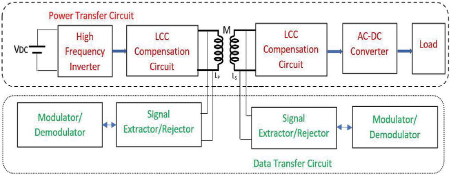
The IPDT system proposed in this work is shown in Figure 1. This system ensures power transmission and full-duplex mode information sharing simultaneously. It includes the power, and the data transfer circuits, and both are connected across the coupled coils parallel manner. A high-frequency inverter converts the DC into an AC signal. Then, the AC signal is transferred to the primary coil via a compensation circuit. On both sides of the contactless power transfer system, compensation circuits are connected. The receiver coil receives the transmitted AC signal, which is then sent to the load via the H-bridge rectifier. The information-sharing circuit includes a series and parallel LC tank circuit-based injector/rejector. These data transfer circuits are connected across the coupled coils parallel manner.
Figure 1 Proposed IPDT system.
Compensation is required in an inductive battery charging system to improve power transfer capabilities and achieve the required power level. The following are some of the advantages of proposed IPDT system:
• No extra controller is needed for incorporating the full-duplex communication between the source and the load. The controller in the power circuit is also used for full-duplex communication. Hence, it is an economical one.
• The dual side LCC topology is adopted in the IPT system and it supports high-level integration at the load side at variable mutual inductance.
• The modulated and demodulated signals are injected/extracted through LC tank circuits. Hence, it is easy for implementing full-duplex communication in an IPT system and supports acknowledgement free communication between the source and the load.
2.1 LLC Based IPT System
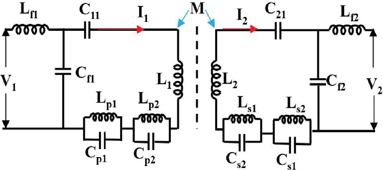
Figure 2 shows the equivalent circuit of the IPT system. Here, L, C are series inductance of the source coil, and L, C are parallel capacitance of the load side coil. V is known as input voltage, and the output voltage is V. The parallel LC tanks are tuned to the modulated signals respective centre frequencies. It creates a high-impedance path for the power signal, which reduces interference from high-frequency modulated signals. Thus, parallel LC tank circuit inductances L, L, L, L, and capacitances C, C, C, C are ignored for power transmission analysis.
Figure 2 LCC topology-based IPT system equivalent circuit.
In [18], the LCC topology is adopted in IPT for transmission of power from the source to load. The parameters of the IPT system are taken from [18] and is given in Table 1. The compensation capacitor’s value and LCC network’s inductor and capacitors values are calculated from the self-inductance of the coils and angular frequency of the power signal. The expressions (1) to (4) describe the currents through inductor L and L and current in the primary side (I) and secondary side (I).
| (1) | ||
| (2) | ||
| (3) | ||
| (4) |
2.1.1 Interference to the power signal
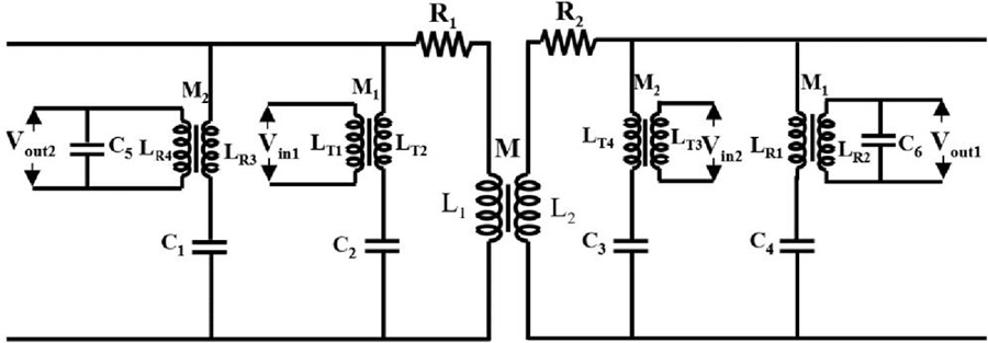
The proposed power transmission and full-duplex mode information sharing circuit is given in Figure 3. From [19] and [20], the reflected impedance model is developed for analyzing the interference between power and data signals. The large difference in frequency of the power and data signals is used to avoid interference between power and data signals. To achieve the resonance condition, the series and parallel LC tank circuit values are calculated from the angular frequency of the information signals. The Equations (5) and (6) describe the receiver coil impedance and reflected impedance to the transmitter coil respectively, which are given below:
| (6) |
Figure 3 Inductive power and data transfer circuit.
In the above, Z is the impedance of the receiver data signal channel and Z is the impedance of the transmitter data signal channel. They are given in equations [7] and [8], respectively.
| (7) | ||
| (8) |
Where Z and Z are the reflected impedances of the transfer circuit. The primary side impedance after addition of information-sharing channel is given in Equation (9),
| (9) |
The primary coil’s voltage is in Equation (10),
| (10) |
Here, i is the current at the primary side. The secondary side voltage is given in Equation (11),
| (11) |
The IPDT system output voltage is given in Equation (12),
| (12) |
The inverter output voltage V and output voltage V are compared and interference in the power signal is analyzed.
2.2 Data Communication Full-Duplex Module
The following sections describe the data communication with the IPT system and digital modulation techniques.
(i) Source to Load Data transmission
The source to load data transmission is realized using series and parallel LC tank circuits. The series LC circuits are connected in parallel with coupled coils at both sides of the contactless power transfer system. It is used to inject and extract the data signal. The primary side data signal is sent from the tank LC circuit to the secondary side via coupling coils. While the parallel LC circuit presents a high impedance path, it also protects the source from high frequency modulated signals. The series and parallel LC circuits satisfy the resonance such that LCLC. The received signal is extracted from the series LC circuit. The parallel LC circuit gives a high impedance path. It prevents the secondary side circuit from receiving the high-frequency data signal.
The current i is calculated from the voltage V and impedance Z. Then, Equation (13) describes load side data communication channel output voltage,
| (13) |
The modulator output V and output voltage V are compared and interference in data signal is analyzed.
(ii) Load to Source Data transmission
The load to source data transmission is realized using series and parallel LC tank circuits. The series LC circuits are connected in parallel with coupled coils at both sides of the contactless power transfer system. It is used to inject and extract the data signal. The secondary side data signal is sent from the tank circuit LC and is used to transfer the data signal from the secondary side to the primary side via coupling coils. While the parallel LC circuit protects the load from the modulated signal, the series and parallel LC circuits satisfy the resonance such that LCLC. The received signal is extracted from the series LC circuit. The parallel LC circuit gives a high impedance path. It prevents the source from receiving modulated signal.
The primary side output voltage of the data communication channel is given in Equation (14),
| (14) |
Where i is the current in the primary side data communication circuit. The modulator voltage V and output voltage V are compared and interference in data signal is analyzed.
(iii) Modulation and demodulation
Full-duplex mode information sharing circuit is employed in the IPDT system to transfer a piece of information to start and stop the battery charging. It also confirms the IPDT system controllability. Phase-shift keying (PSK) and Amplitude shift keying (ASK) are connected separately with the LCC topology-based WPT system.
In ASK modulation method, the amplitude of the carrier signal is varied by the digital binary sequence. The ASK-OOK (on-off keying) is used to verify the full-duplex mode information sharing in the IPDT system. In this, the 1.44 MHz high frequency modulated signal is used for binary data 1 while no signal is transferred for binary 0. The ASK-OOK is described in Equation (15):
| (15) |
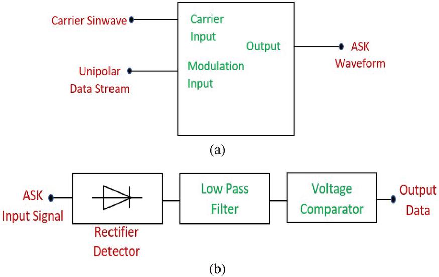
Figure 4 shows the ASK modulator and demodulator. The ASK signal is generated by the balanced modulator. At any given time, the output voltage is the product of the two input voltages. One of the inputs is a high-frequency AC coupled carrier wave. The other input, which is the data signal to be transmitted, is DC coupled. It’s referred to as modulating signal.
Figure 4 ASK (a) modulator (b) demodulator.
The method to demodulate the ASK modulation results in an increased simplicity at the receiver side. The received ASK demodulated signal is given to the rectifier and then passed through the low pass filter. The resulting waveform is squared up, and output is the actual data stream.
In PSK, the phase of the high-frequency carrier wave is altered when modulating signal bit changes from 1 to 0 and 0 to 1. But there is no change in the frequency of the modulated signal. The PSK is described in Equation (16):
| (16) |
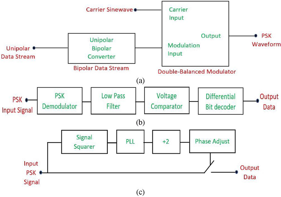
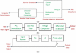
Figure 5 shows the PSK modulator and demodulator. The PSK signals are generated in a balanced modulator. The modulator output is a sinewave. It is in phase or out of phase with the carrier input accordance with positive or negative level of modulating signal respectively.
Figure 5 (a) PSK modulator (b) PSK demodulator (c) PSK receiver system.
The signal squarer changes the phase of modulated PSK signal from 0 and 180 to 0 and 360. It is a technique for multiplying an input signal by itself. Here, the phase transitions are removed from the actual PSK signal. The PLL creates a frequency-matched clean square wave output, which is then delivered to the divided by 2 circuits. The phase adjusts circuit modifies the digital signal phase and allows the actual PSK wave to pass over the detector.
The demodulated signal is passed through a low pass filter, which rounds the data signal for use in digital processing. Then, the original data signal gets from the differential bit encoder and voltage comparator.
ASK and PSK are digital modulation techniques. In ASK, the amplitude of the high-frequency carrier signal is varied in accordance with the digital input signal. The process of changing the carrier signal phase in accordance with the digital input signal is known as PSK. The probability of error is lesser, and signal-to-noise ratio (SNR) is higher in PSK compared with ASK. Further, PSK is more power-efficient than ASK. Thus, PSK is a suitable digital modulation technique in the RF communication system.
3 Simulation Results
The transmitter and receiver coils are modelled in the FEM Ansys maxwell simulation tool. The computed results are now discussed.
3.1 FEM Model
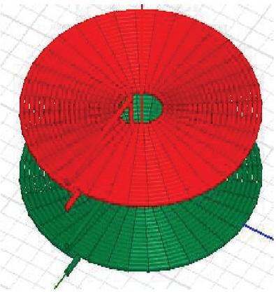
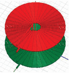
Figure 6 shows the designed coupled coil structure. The proposed system used Litz wire in coupled coils structure. Mutual inductance (MI) gives a key role in designing an effective WPT system. It depends on Litz wire diameter, the radius of the connected coupled coils radius, turns separation, coupled coils’ number of turns. FEM 3D modelling is used to develop the proposed coupled coils structure, and the findings are then used in 2D modelling.
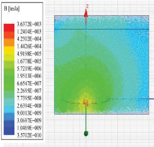
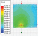
The specifications of the coupled coils are given in Table 1. To compute the MI of connected coupled coils, the distance between coupled coils is varied vertically. The MI is computed, and Figure 7 shows the magnetic flux density distribution for 50 mm between connected coupled coils of the IPDT system. The mutual inductance value for 50 mm distance is used for creating an effective contactless power transmission system.
Figure 6 Designed coupled coil structure in FEM.
Table 1 Coupled coils specification
| Parameter | Specification |
| The transmitter coil’s number of turns | 26 |
| The receiver coil’s number of turns | 26 |
| The transmitter coil’s self-inductance in H | 230 |
| The receiver coil’s self-inductance in H | 230 |
| Mutual Inductance in H (50 mm) | 48.26 |
| Transmitter side capacitance in F | 0.329 |
| Receiver side capacitance in F | 0.329 |
| Transmitter series inductance in H | 37.79 |
| Receiver series inductance in H | 37.79 |
| Conductor radius in mm | 5 |
| Coil Diameter in cm | 30 |
| Type | Circular |
| Voltage | 60 |
| Frequency in kHz | 20 |
Figure 7 Coupled coils magnetic flux density distribution at 50 mm.
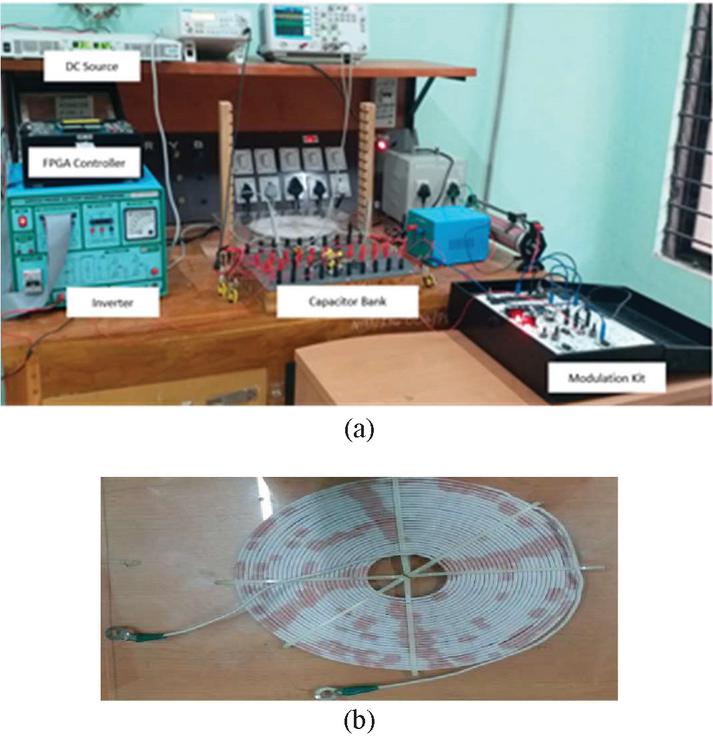
Figure 8 (a) Photograph of experimental setup (b) Litz wire coil used in IPDT system.
4 Measurements and Validation
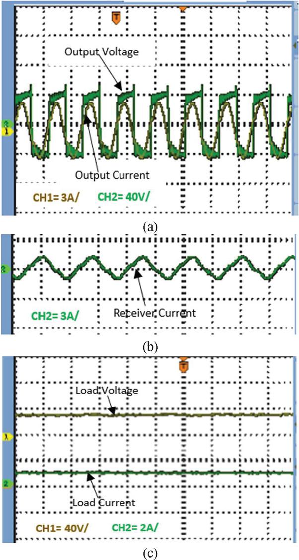
The IPDT system developed is shown in Figure 1, and a snapshot of it is found in Figure 8. The experimental setup consists of a DC source, SiC-based inverter, spiral circular coupled coils, compensation circuits, and AC to DC conversion circuit. The LCC compensation circuit is connected at both transmitter and receiver sides. The gating pulses are generated from the FPGA controller and are supplied to the inverter set at a frequency of 20 kHz. The primary side coil receives the inverter’s output, while the secondary side coil receives the transferred signal, which is then sent to the rectifier and filter. From the fabricated hardware, waveforms were recorded at different points of the circuit and are given in Figure 9. The input impedance phase angle is observed to be 13 for a 50 mm distance between the proposed coupled coils. At a constant load of 12, the inverter voltage and current are measured for an MI value of 48.26.
Figure 9 Measured results (a) output voltage and current of inverter (b) current at receiver coil and (c)load voltage and current.
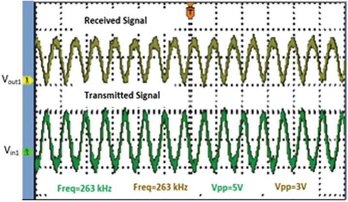
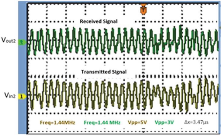
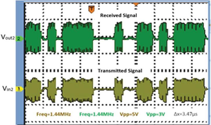
The full-duplex communication channel is used for data transmission on both the transmitter and receiver sides. Table 2 gives the LC tank circuit specification. From Figure 1, the source side sinusoidal signal of frequency 263 kHz is generated. It is inserted via a series LC circuit and the signal is received at the load side. Figure 10 shows the transmitted and received waveforms. The load-side PSK signal of frequency 1.44 MHz is generated. It is inserted via a series LC circuit and the signal is received at the source side through a series LC circuit. Figure 11 shows the transmitted and received waveforms. The same procedure is repeated for analyzing the transmission of ASK and sinusoidal signals. Figure 12 shows the ASK transmitted and received signals. The data transmission delay x is around 3.47 s, which is indicated in Figures 11 and 12.
Table 2 LC tank circuit specification
| Parameter | Specification |
| Forward Data Transfer Channel: | |
| Transformer inductance L & L in H | 1.66 |
| Transformer inductance L & L in H | 1.66 |
| Inductance L and L in H | 1.66 |
| Capacitance C, C, C, C & C in F | 0.22 |
| Frequency in kHz | 263 |
| Reverse Data Transfer Channel: | |
| Transformer inductance L & L in H | 0.18 |
| Transformer inductance L & L in H | 0.18 |
| Inductance L and L in H | 0.18 |
| Capacitance C, C, C, C & C in F | 0.068 |
| Frequency in MHz | 1.44 |
Figure 10 Source side signals.
Figure 11 Load-side PSK signals.
Figure 12 Load side ASK signals.
The power and bitrates values were obtained from the IPDT system for 50 mm and 100 mm distances between coupled coils i.e., two different values of coupling coefficient and mutual inductances. The value of coupling coefficient and mutual inductances decrease while changing the distance between coupled coils from 50 mm to 100 mm. Under resonance conditions, the reactive components of the transmitter and receiver coils are cancelled by added compensation circuits, while the LC tanks in data circuits provide a high impedance path to the power signal. As a result, the 46.6 W and 35.2 W of power were transferred from the source to the load for 50 mm and 100 mm respectively. In case of heavy misalignment that is 45%, the value mutual inductance changes from 48.26 H to 22.48 H. It affects the value of reflected capacitor and changes in resonance region. As a result, the inductive coil current decreases. Moreover, ASK and PSK communication circuits are individually connected with the IPDT system. The peak voltage of the PSK is more than the peak voltage of the ASK modulation scheme. It is shown in Table 3.
Table 3 Data rates, output power, and data signal peak voltage for various distances
| Distance(mm) Between | Output Power | Data Rate | PSK Signal | ASK Signal |
| Coupled Coils | in Watts | in kbps | in Volts | in Volts |
| 50 | 46.6 | 288 | 1.6 | 1.3 |
| 100 | 35.2 | 288 | 0.75 | 0.6 |
Table 4 Performance comparison between proposed and available works
| Literature | Power Rating in Watts | Data Rate in kbps | Mode of Communication |
| [19], 2016 | 250 | 19.2 | Half-duplex |
| [12], 2018 | 40 | 230 | Half-duplex |
| [15], 2019 | 354 | 19.2 | Half-duplex |
| [21], 2021 | 600 | 80 | Full duplex |
| (This work) | 46.6 | 288 | Full duplex |
The simple passive components are used in the developed IPDT system. Thus, the proposed IPDT system is easy to implement and economical. In addition, the data transmission initiation is possible without any acknowledgment between the transmitter and the receiver sides data communication module. The performance comparison table is given in Table 4. From the table, the developed IPDT system has low latency and the data rate reaches 288 kbps. Moreover, it supports full-duplex mode communication between the source and the load. It is a good solution for WPT systems applications with low and medium power.
5 Conclusion
In this paper, ASK and PSK modulation techniques for full-duplex communication in LCC topology-based WPT systems were analyzed and compared. The mutual inductance and flux density distribution were calculated using FEM Ansys maxwell and the IPT system designed effectively. The series and parallel tank circuit’s properties are used to design full-duplex communication in the IPT system. Besides, the interference between power and data signals was analysed through the reflected impedance-based model. Furthermore, the power and data are transferred simultaneously through single coupled coils. The 46.6 W and 35.2 W of power transferred from the source to the load for 50 mm and 100 mm respectively. While the data rate reaches 288 kbps for both distances. Further, the peak voltage is more for the PSK modulation technique than the ASK modulation technique. Thus, PSK is a suitable and power-efficient technique in the WPT system.
References
[1] A. Khaligh, S. Dusmez, “Comprehensive topological analysis of conductive and inductive charging solutions for plug-in electric vehicles”, IEEE Transactions Vehicular Technology, 2012, 61(8):3475–3489.
[2] G. A. Covic, J. T. Boys, “Modern trends in inductive power transfer for transportation applications”, IEEE Journal of Emerging Selected Topics in Power Electronics, 2013,1(1):28–41.
[3] S. Li, C. Mi, “Wireless Power Transfer for Electric Vehicle Applications”, IEEE Journal on Emerging and Selected Topics in Power Electronics, 2015, 3(1):4–17.
[4] A. A. S. Mohamed, A. A. Marim, O. A. Mohammed, “Magnetic design considerations of bidirectional inductive wireless power transfer system for EV applications”, IEEE Transactions on Magnetics,2016, 53(6):1–8.
[5] L. Huang, G. Meunier, O. Chadebec, “General integral formulation of magnetic flux computation and its application to inductive power transfer system”, IEEE Transactions on Magnetics, 2017, 53(6):14–21.
[6] C. C. Mi, G. Buja, S. Y. Choi, and C. T. Rim, “Modern advances in wireless power transfer systems for roadway powered electric vehicles,” IEEE Trans. Ind. Electron., vol. 63, no. 10, pp. 6533–6545, Oct. 2016.
[7] Đurić, Radivoje, and Milan Pajnić. “Design of compensation network with variable inductance wide variation of coupling coefficient in inductive power transfer.” International Journal of Circuit Theory and Applications 47, no. 11 (2019): 1786–1799.
[8] Q. Hu, D. Hu, B. Duan, and J. He. “A fully implantable stimulator with wireless power and data transmission for experimental investigation of epidural spinal cord stimulation”, IEEE Trans. Neural Syst. Rehabil. Eng, 2015, 23(4):683–692.
[9] T. Bieler, M. Perrottet, V. Nguyen, Y. Perriard, “Wireless power and data transmission”, IEEE Trans. Ind. Electron, 2002, 38(5):1266–1272.
[10] K. Dostert. Powerline communications. Englewood Cliffs, NJ: Prentice-Hall,2001.
[11] M.H. Shwehdi, A.Z. Khan, “A Power line data communication interface using spread spectrum technology in home automation”, IEEE Transaction on Power Delivery, 1996, 11(3):1232–1237.
[12] Xiaofei, Chunsen Tang, Xin Dai, Pengqi Deng, Yugang Su, “An Inductive and Capacitive Combined Parallel Transmission of power and Data for Wireless Power Transfer Systems”, IEEE Transactions on Power Electronics, 2018, 33(6):4980–4991.
[13] Chih-Cheng Huang, Chun-Liang Lin, Yuan-Kang Wu, “Simultaneous Wireless Power/Data Transfer for Electric Vehicle Charging”, IEEE Transactions on Industrial Electronics, 2017, 64(1):682–690.
[14] Jin-Guk Kim, Guo Wei, Man-Ho Kim, Hyok-Su-Ryo and Chunbo Zhu, “A Wireless Power and Information Simultaneous Transfer Technology Based on 2FSK Modulation Using the Dual Bands of Series-Parallel Combined Resonant Circuit”, IEEE Transactions on Power Electronics, 2019, 34(3):2956–2965.
[15] Ji. L. Wang, C. Liao and S. Li, “Simultaneous Wireless Power and Bidirectional Information Transmission with a Single-Coil Dual-Resonant Structure”, IEEE Transactions on Industrial Electronics, 2019, 66(5):4013–4022.
[16] J. Wu, C. Zhao, Z. Lin, J. Du, Y. Hu, and X. He, “Wireless power and data transfer via a common inductive link using frequency division multiplexing”, IEEE Trans. Ind. Electron. 2015, 62(12):7810–7820.
[17] Zhongnan Qian, Rui Yan, Jiande and Xiangning He, “Full-Duplex High-Speed Simultaneous Communication Technology”, IEEE Transactions on Power Electronics. 2019, 34(10):9369–9373.
[18] P. Srinivasa Rao Nayak, Dharavath Kishan, “Performance analysis of series/parallel and dual side LCC compensation topologies of inductive power transfer for EV battery charging system”, Front Energy, 2020, 14(1):166–179.
[19] Yue Sun, Peng-Xu Yan, Zhi-Hui Wang, Ying-Ying Luan, “The Parallel Transmission of Power and Data with the Shared Channel for an Inductive Power Transfer System”, IEEE Transactions on Power Electronics, 2016, 31(8):5495–5502.
[20] T. Manikandan, P. Srinivasa Rao Nayak, K. Sundareswaran. A new technique for power transmission and full duplex communication employing SN IPT system. Int J Circ Theor Appl. 2021;1–12. doi: 10.1002/cta.3165.
[21] Yuan Shuang Fan, Yue Sun, Xin Dai, Zhiping Zuo and Anhong You, “Simultaneous Wireless Power Transfer and Full-Duplex Communication with a Single Coupling Interface”, IEEE Transactions on Power Electronics, vol. 36, No. 6, June 2021.
Biographies

T. Manikandan received the B.E. degree in electronics and communication engineering from Anna University, Chennai, Tamil Nadu India, in 2005; and the M.E. degree in Applied Electronics, from Anna University, Chennai, Tamil Nadu, India, in 2008. Currently, he is pursuing a Ph.D. degree in electrical and electronics engineering from the National Institute of Technology, Tiruchirappalli, Tamil Nadu, India. His research interests include power electronics and wireless power and data transfer systems.

Panugothu Srinivasan Rao Nayak received the B.Tech. degree in electrical and electronics engineering from Bapatla Engineering College (BEC), Bapatla, Guntur, in 2001; the MTech. degree in energy systems from Jawaharlal Nehru Technological University (JNTU), Hyderabad, Telangana, India, in 2006; and the Ph.D. degree in electrical engineering from the National Institute of Technology, Tiruchirappalli, Tamil Nadu, India, in 2014. Currently, he is an Assistant Professor with the Department of Electrical and Electronics Engineering, National Institute of Technology. His research interests include power electronics and drives, biologically inspired optimization techniques, and wireless power transfer systems.

Sishaj P. Simon received the B.Eng. degree in electrical and electronics engineering from Bharathiar University, Coimbatore, Tamil Nadu, India, in 1999 and the M.Eng. degree in applied electronics from Bharathiar University, Coimbatore, Tamil Nadu, India, in 2001; and the Ph.D. degree in power system engineering from Indian Institute of Technology (IIT), Roorkee, Uttarakhand, India, in 2006. Currently, he is an Associate Professor with the Department of Electrical and Electronics Engineering, National Institute of Technology (NIT). His research interests include the area of power system operation and control, power system planning and reliability, artificial neural networks, fuzzy logic systems, and application of meta-heuristics, and intelligent techniques to power systems.

Kinattingal Sundareswaran received the B.Tech. (Hons.) degree in electrical and electronics engineering power electronics from the University of Calicut, Calicut, Kerala, India, in 1988 and MTech. (Hons.) degree from the University of Calicut, Calicut, Kerala, India, in 1991; and the Ph.D. degree in electrical engineering from Bharathidasan University, Tiruchirappalli, Tamil Nadu, India, in 2001. He is currently a Professor with the Department of Electrical and Electronics Engineering, National Institute of Technology, Tiruchirappalli, Tamil Nadu, India. His research interests include power electronics, renewable energy systems, and biologically inspired optimization techniques.
Distributed Generation & Alternative Energy Journal, Vol. 38_2, 547–568.
doi: 10.13052/dgaej2156-3306.3828
© 2023 River Publishers
