Design and Analysis of Quasi-Y Source High Gain DC/DC Resonant Converter for Renewable Energy Applications
Sugali Harinaik* and Shelas Sathyan
National Institute of Technology Tiruchirappalli, Tamil Nadu, India
E-mail: Harinaik223@gmail.com; shelassathyan@yahoo.co.in
*Corresponding Author
Received 25 January 2022; Accepted 02 May 2022; Publication 03 January 2023
Abstract
This paper proposes a magnetically coupled partial resonant isolated quasi-Y source DC/DC converter. Here, to achieve soft switching, there is no additional auxiliary circuits or magnetic components are used. By making use of transformer’s parasitic elements like winding capacitance (C) and leakage inductance (L), zero current switching (ZCS) is obtained at the turn-off instant of all MOSFETs. Hence, the converter can operate at a higher frequency, so that compact size and good efficiency are feasible. This converter inherits all the conventional impedance source converter features, and a higher gain is obtained by using three winding coupled inductor and isolation transformer with small shoot-through duty (d). Hence, the continuous input current (CIC) and galvanic isolation feature of this converter is most suitable for renewable energy applications. Also, the output voltage is regulated by changing the switching frequency. Finally, a 300 W prototype is designed and tested in the laboratory. The simulation, experimental results with mathematical and design analysis are provided.
Keywords: Renewable energy resources, impedance source converters, high voltage gain, DC/DC converters, zero current switching (ZCS).
1 Introduction
Nowadays, demand for renewable energy resources is growing more popular due to extensive utilization of fossil fuels such as coal, gas, and oil. Hence, which leads to major environmental pollution, greenhouse gas emissions, and it has a significant global impact. However, there is a considerable mismatch between the availability of fossil fuels and energy demand. So to meet the energy demand and ecological concerns, renewable energy resources are best alternatives. These sources are mainly wind, Biomass, fuel cells, photovoltaic (PV) systems, etc. [1, 2]. Among these, Solar PV and Wind are good candidates because their universal availability, emission-free, and fuel cell are also most significant due to higher conversion efficiency. The output voltage of the aforementioned renewable energy resources is low, so to interface with DC grids, high step-up DC/DC converters are required [3]. High voltage gain can be achieved by using the traditional DC/DC boost converter. However, the converter needs to operate at higher duty (close to unity). So that, components will suffer from higher current and voltage stress. Conduction losses in the converter are more because of the longer conduction of the active switch. Furthermore, the diodes at the output side will conduct very short intervals, resulting in significant reverse recovery issues [4].
In the literature, different types of non-isolated and isolated topologies are available for high voltage boosting [5–7]. By using the coupled inductors, high gain can be achieved. In [8], a soft switched non-isolated three winding coupled inductor type DC/DC converter is presented for high step up renewable energy applications. Here, the three-winding coupled inductor creates more degree of freedom to attain high voltage gain. In renewable energy resources, isolated converters are used for high step-up voltage to overcome higher duty ratio and safety concerns. The isolated topologies like full-bridge, flyback, push-pull, etc., can obtain high voltage gain by changing the transformer’s turns ratio [9–12]. However, the converters in [9, 11] are high gain voltage fed converters (VFC), whereas in [10, 12] are current fed converters (CFC). These converters have some limitations; in the VFC, there is a prohibition with short through of switches in the same leg, to avoid this small dead band is provided in between them. Whereas in CFC, the switches (top & lower) in the same leg triggered together (Shoot through). Otherwise, DC inductor gets opened and it causes high voltage stress on switches and the main circuit gets damaged. VFC are buck type, whereas CFC are boost converters and can’t be used as buck-boost converters. To overcome this, impedance source converters (ISC) are introduced and here switches in the same leg can be short-circuited or open circuited. Hence, the ISC can be operated as buck type, boost type, or both buck-boost types [13–15]. Furthermore, based on topological structure, the ISC can be classified as non-isolated [16–19] and isolated [21–27] type converters. To achieve higher gain a three-winding coupled inductor Y-source converter is proposed in [17], it has more freedom to attain high gain. However, due to the DIC nature of this converter not a good candidate for PV and fuel cell systems. Hence, to overcome this a CIC quasi-Y-source converter is presented in [18]. Furthermore, to reduce the voltage stress on the components and higher voltage gain a modified Y-source DC/DC converter is presented in [19]. Here, all the aforementioned converters are non-isolated, and not suitable for PV, fuel cell systems. Here galvanically isolated impedance source DC/DC converters are present due to safety concerns in PV systems and grid-tied converters.
The first isolated impedance source DC/DC converter was introduced in 2009 [20]. It inherits all the features of the conventional Z-source network. In [21], the reliability and efficiency are improved with a reduced number of switches. However, these converter’s DIC nature is not recommended for PV and fuel cell applications. To resolve this issue, researchers are introduced a CIC isolated quasi-Z source DC/DC converter [22, 23]. Hence, the CIC feature of these converters is mainly preferred for renewable energy resources. Furthermore, magnetically coupled ISC are presented in [24, 25] to improve the gain. The converter in [24], gain is improved by coupled inductor and isolation transformer with reduced switch count. Moreover, due to the DIC nature, this converter is not preferred. In [25], researchers developed a magnetically coupled CIC Y-source DC/DC converter. Moreover, all aforementioned converters are hard switched converters so that turn-on and turn-off losses are more and impact on the overall converter efficiency. Researchers are made efforts to develop soft switching in impedance source DC/DC converters [26–28]. However, the converters in [26, 27] are soft switched and high gain these are not preferred due to non-isolated type. In [28] soft switched, isolated high gain ISC is presented with computerized simulation.
This paper’s main objective is to design high efficieny, compact size, low voltage stress on semiconductor devices and higher power density DC/DC converter to interface renewable energy resources. In the literature, the soft switched frequency modulated high gain DC/DC impedance source converters are not extensively investigated. In this paper, authors are made efforts to develop soft switched frequency modulated impedance source DC/DC converters. To obtained higher gain a magnetically coupled three winding coupled inductor and high frequency transformer is used. Here, output voltage is regulated by varying the switching frequency. Furthermore, soft switching (ZCS) is obtained by properly selecting LC tank, which causes the partial resonance during shoot through instant, and all the active devices (MOSFETs) are turned off with ZCS. There are no additional magnetic components, active and passive devices are used for achieving soft switching (ZCS). This improves the overall efficiency of the converter. Since converter having soft switching feature high frequency operation is possible. Hence magnetic component and other filter capacitor size can be reduced which enhance the power density. Also due to ZCS, the turn off voltage spikes on switches (which is typical problem in current fed converters) are eliminated. This converter inherits all the features of ISC, and it overcome the demerits of a conventional converter [13]. In Section 2 steady state operation and description of the proposed converter is discussed. The design analysis, simulation and experimental results are presented in Sections 3 and 4.
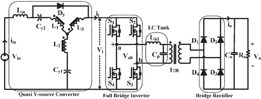
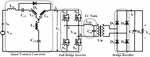
Figure 1 Proposed isolated quasi-Y source DC/DC converter.
2 Discerption and Operation of the Proposed Converter
In Figure 1, the proposed isolated quasi-Y source DC/DC converter is shown. This converter consists of three winding coupled inductors (L, L, and L) having N, N, and N number of turns in the respective windings, two capacitors C, C, input inductor L and diode D. The two DC blocking capacitors C and C are used to prevent core saturation in the Y-source coupled inductor. The input inductor is connected in series with the voltage source, and the blocking diode D is connected between the drain of the active switch and the negative terminal of the capacitor C. The output of the quasi-Y source converter is connected to the bridge inverter. The primary and secondary sides of the isolated high-frequency transformer (HFT) are connected to the inverter and rectifier bridges. Here, the LC tank is formed by utilizing the transformer’s parasitic like leakage inductance (L) and winding capacitor (C parasitic capacitor). However, partial resonance is obtained by proper selection of LC tank. This allows all switches in the inverter will turn off with ZCS. The output voltage is controlled using the frequency modulation technique while maintaining the shoot-through duty ratio (d) constant. Here, to utilize the CIC and extensive features of the impedance network presented in [18] is taken. Moreover, the converter in [18] is a non-isolated, PWM-controlled, and hard switched converter. Here, efforts are made to develop a soft switched isolated and frequency modulated high gain converter for renewable energy applications.
2.1 Configuration of Quasi-Y Source Topology [18]
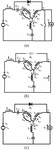
Figure 2(a) presents the equivalent circuit of the CIC quasi-Y source converter. It has three coupled inductors (L, L, and L), one input inductor L, one blocking diode D, two dc capacitors C, C, and one active switch S. Here, L is the magnetizing inductance of the Y-source coupled inductor with respect to winding one, and V is the voltage across this winding 1. N, N, and N are the number of turns in each winding. From Figure 2(b), (c), this converter mainly operates in shoot-through and non-shoot through states respectively.
The shoot-through state is depicted in Figure 2(b), in this state, active switch S is conducting, and diode D is OFF. During this state, input inductor L and magnetizing inductor L are charged. By analysing the circuit, the steady-state analysis can obtain as follows.
| (1) | |
| (2) |
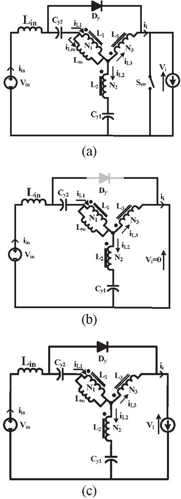
Figure 2 Equivalent circuit (a) CIC quasi-Y source converter, (b) Shoot through state, (c) Non-shoot through state.
Non-shoot through state is presented in Figure 2(c). During this state, switch S is OFF, and diode D is conducting. By analysing the circuit, the following expressions are obtained.
| (3) | |
| (4) | |
| (5) | |
| (6) |
Here, , are turns ratios of N, N, N and is the DC link voltage.
By state-space averaging, from (1) and (3) the resultant can obtain as follows.
| (7) |
Applying state-space averaging at input inductor L, by using (2), (4) and after solving the below equation, we will obtain (8).
| (8) |
By using (7) and (8), the simplified individual capacitor voltages are obtained as
| (9) | ||
| (10) |
By substituting (3), (9), and (10) in (6), the resultant DC link voltage can be obtained as follows.
| (11) |
Here, is the winding factor of quasi-Y source coupled inductor.
| (12) |
For each selected value of , various combinations of turns ratios N: N: N are realized, illustrated in the Table 1.
From Equation (11), the allowable shoot through duty variation is given as follows
| (13) |
The relation of d and conventional duty (D) is given as below.
| (14) |
Table 1 Realization of Shoot-through duty ratio (d) and winding factor () with different turns ratios (N: N: N)
| Conventional Duty Range (D) | (N: N: N) Turns Ratio | ||
| 2 | 1/2 | 0.5 D 3/4 | (1:3:1), (2:4:1), (3:5:1) |
| 3 | 1/3 | 0.5 D 4/6 | (1:4:1), (3:3:1), (2:4:2) |
| 4 | 1/4 | 0.5 D 5/8 | (2:2:1), (1:3:2), (5:3:1) |
| 5 | 1/5 | 0.5 D 6/10 | (3:2:1), (2:3:2), (1:4:3) |
| 6 | 1/6 | 0.5 D 7/12 | (4:2:1), (3:3:2), (2:4:3) |
| 7 | 1/7 | 0.5 D 8/14 | (4:3:2), (5:2:1), (3:4:3) |
| 8 | 1/8 | 0.5 D 9/16 | (5:3:2), (6:2:1), (3:5:4) |
2.2 Steady State Analysis and Modes of Operation of the Proposed Converter
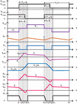
The steady-state waveform of the proposed converter is presented in Figure 3. Here, by utilizing the transformer’s parasitic L and C, soft switching (ZCS) is achieved at the turn-off instant. To regulate the output voltage, here frequency modulation technique is implemented. Here constant shoot through duty (d) is chosen for soft computation of power MOSFETs. The gate signals, pair of V, V, and pair of V, V is 180 phase-modulated each other with small D. The converter analysis is studied for the first half cycle over five operating modes with detailed discussion is given. The equivalent circuit operation is depicted in Figure 4.
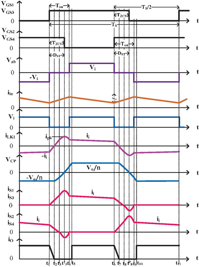
Figure 3 The steady-state waveforms of the quasi-Y source DC/DC impedance converter.
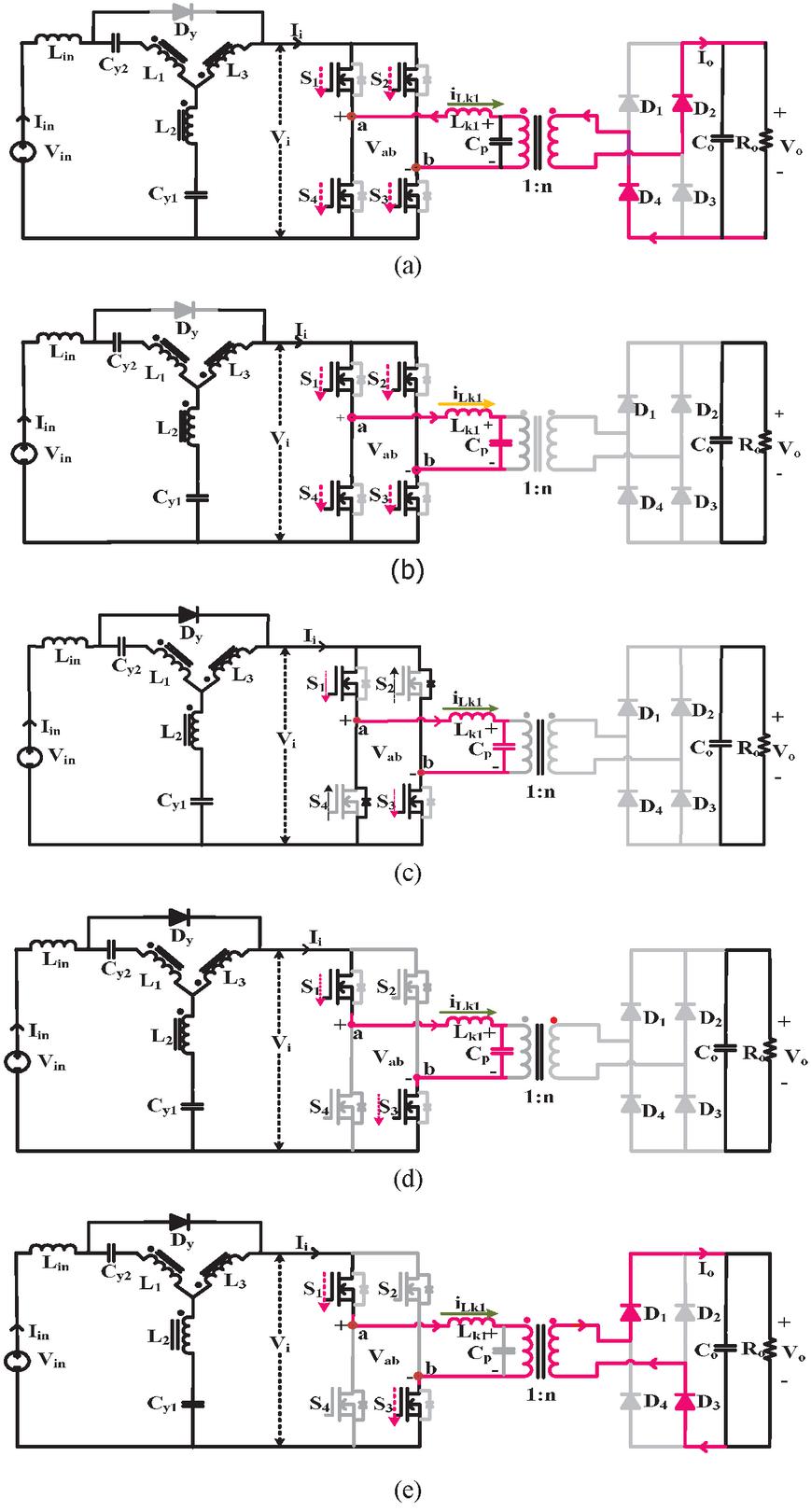
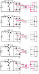
Figure 4 Operating modes of proposed topology (a) Mode I, (b) Mode II, (c) Mode III, (d) Mode IV, (e) Mode V.
Mode I: [Figure 4(a)]
This mode is started at t. Before that, power MOSFETs S, S are in conduction, and energy is transferred from source to load. At t t, the MOSFET pairs S and S are triggered, and all the MOSFETs are under conduction. In a bridge rectifier, D and D are conducting, and D and D are off. The diode D in the impedance network is also off. Here, the leakage inductor L and input inductor L starts charging. The current flows through L and L linearly increases. The current through the power MOSFETs S, S increases, whereas in S, S are decreased, and these can be observed in Figure 3. The voltage across C and current through L is given as follows.
| (15) | |
| (16) |
Time duration for this Mode I is obtained as follows
| (17) |
Here n is the turns ratio of HFT, and this mode ends at t when L current reaches zero.
Mode II: [Figure 4(b)]
This mode will start at t, when diodes D, D in the bridge rectifier are reverse biased. All the power MOSFETs are conducting, and D is off. The transformer’s parasitic L and C form the LC tank cause resonance in the circuit. The current through switch pairs S and S is still increasing, and the switch pairs S and S are decreasing.
The current through L is given as
| (18) | |
| (19) | |
| (20) |
Here, z, f, and w are characteristic impedance of the network, resonant frequency, and angular frequency respectively. The time duration for this mode is given in (21)
| (21) |
Mode III: [Figure 4(c)]
This mode will start at t when the value of leakage inductor current is equal to I. At this instant, the current through the power MOSFETs S, S is zero and which are turned off with ZCS. Currently, the conducting devices are S, S, body diodes of S, S, and D. The current through L reaches the peak value I at t t, whereas voltage across the C is zero.
| (22) |
Here I is the peak value of L current, and the time duration () is given by
| (23) |
Mode IV: [Figure 4(d)]
At t t, when the L current reaches to this mode will start. This instant body diodes of S, S turned off, and the power MOSFETs S, S, diode D are still conducting. Here at the end of this mode parasitic capacitor C is fully charged with I current. The time taken for this mode is given as follows
| (24) |
Mode V: [Figure 4(e)]
During this mode, C is fully charged with voltage of V and the diodes D, D in rectifier bridge start conducting. Here, the power MOSFETs S, S and D are in conduction. Here energy is transferring to the load and leakage inductor current is equal to the .
| (25) |
The time duration for half switching period (T/2) is equal to total time duration of Mode I to V, and it is given as follows
| (26) |
3 Design Analysis of the Quasi-Y Source Converter
In the CIC quasi-Y source converter, the coupled inductor is represented by a three-winding ideal transformer with leakage inductance and magnetizing inductance of each winding. Here all the power MOSFETs and diodes are ideal.
3.1 Voltage Gain (M)
The average output current () is given as
| (27) |
From the power balance equation
| (28) | |
| (29) |
Here is the efficiency of the converter, n is the turns ratio of the HFT, and R is the full load resistance.
By using (26), (27), and (29), the voltage at the output side is obtained as
| (30) |
The output voltage can be obtained by substituting the Equations (17), (23), and (25) in (30). Hence it is derived as follows.
| (31) |
The proposed converter gain is obtained as
| (32) |
By using (11), (31), and (32) the resultant gain of the proposed converter is obtained as
| (33) |
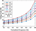
Here, , , , f Normalized frequency, f Switching frequency, f Resonant frequency, M Gain of the converter, r Normalized resistance, R Full load output resistance, Z=Characteristic impedance. The gain of the converter for the ideal case depends on the turns ratio of the transformer (n), winding factor (12), and shoot through duty (d). The gain of the proposed converter is shown in Figure 5 at different turns ratio of the transformer. The converter gain is increased by increasing the turns ratio of the transformer.
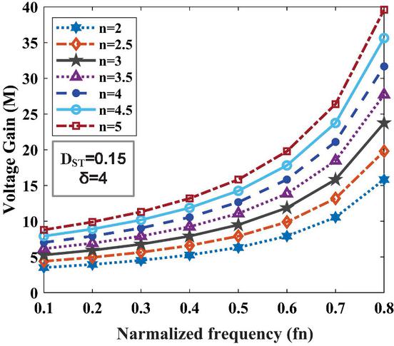
Figure 5 Gain curve with normalized frequency (f).
3.2 Design of Input Inductor
The input inductor can be designed based on the current ripple. The current ripple at the input inductor is given as
| (34) |
From Equation (5)
| (35) | |
| (36) |
3.3 Condition for ZCS
Here the LC tank must be designed properly to obtain ZCS. The L and C stored energy is mainly responsible for achieving soft switching, and selected value Z should satisfy the following condition.
| (37) |
3.4 and Design
The transformer parasitic’s L and C must be chosen carefully to accomplish ZCS. The characteristic impedance (Z) is obtained from Equation (37). By utilizing Equations (20) and (37), the L, C parameters are calculated. The selected value of Z should satisfy the ZCS condition (37).
3.5 Voltage Stress of MOSFETs and Diodes
The voltage stress on MOSFETs and output diodes is given in (37), (38). From (37), the voltage stress on all MOSFETs is dependent on the output voltage and the number of turns in the HFT. The diodes voltage stress is the same as the output voltage.
| (38) | |
| (39) |
4 Discussion on Simulation/Hardware Results
The performance of a quasi-Y source high gain DC/DC resonant converter using PSIM Simulink, and hardware prototype is presented. Here, the converter is designed for 300 W power and, the input voltage varies (40–60) V and output is regulated to standard 380 V DC grid voltage. Here output voltage is regulated by varying switching frequency at constant shoot through duty (d). The switching frequency is varied from 85 kHz to 190 kHz. When the input voltage is 40 V, to regulate the rated output voltage converter is operated at 190 kHz and when input voltage is 60 V to regulate the rated output an 85 kHz switching frequency is applied. In Table 2, the converter specifications and other design parameters are given.
Table 2 Components and parameters specifications
| Parameter | Specification Value |
| Rated Power (P) | 300 W |
| Input voltage (V) | 40–60 V |
| Output voltage (V) | 380 V |
| Switching frequency (f) | 85–190 kHz |
| Shoot through duty (d) | 0.15 |
| Input inductor (L) | 2 mH |
| Capacitors | CF, CF, CF |
| Power MOSFETs | IRFP4227pbf, R m |
| Diodes | RHRG75120 |
| Coupled Inductor (N: N: N) | EE55/28/21 Ferrite core (16:16:8) |
| Winding Factor () | 4 |
| HFT (N: N) | EE42/21/15 Ferrite core (4: 20) |
| L | 0.85 H |
| C | 0.18 F |

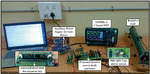
Figure 6 Experimental prototype of Quasi-Y source DC/DC converter.
The experimental photograph of the converter is shown in Figure 6. The coupled inductor is designed using EE55 gapped ferrite core with a 16:16:8 number of turns. All the windings are wound tightly in Y shape manner. EE42 ferrite core is used for HFT. Hence, the tight coupling of the inductor and transformer results in less parasitic resistance and leakage in each winding. Moreover, to reduce the skin effect and ac resistance of winding Litz wires are used. For generating gate signals, (TMS320F28335) TI supported C2000 development kit is used. All the active and passive components are selected to achieve lower losses.
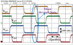
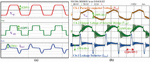
The simulation and experimental tests are performed at rated power of 300 W with 48 V input voltage. The output voltage is regulated to 380 V by varying the switching frequency up to 150 kHz. The switching pulses of the proposed topology with small shoot-through duty (d) presented in a dotted circle and operating at 150kHz switching frequency are shown in Figure 7. Here, the gate pulse of MOSFETs 1, 3, and MOSFETs 2, 4 are modulated with a 180 phase difference.
The key waveforms of simulation results are shown in Figures 8(a), 9(a), 10(a), 11(a), respectively. The developed prototype experimental results are shown in Figures 8(b), 9(b), 10(b), 11(b). Here, the simulation and experimental test are done at the rated condition of the developed converter. Both simulated and experimental results are found to be identical.

Figure 7 Gate pulse of the proposed converter at switching frequency f kHz.
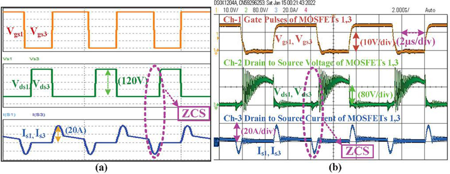
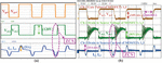
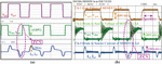
Figure 8 Standard waveforms obtained from (a) simulation and (b) Experimental results of gate signals, voltage stress, current through the pair of switches S, S at rated condition.
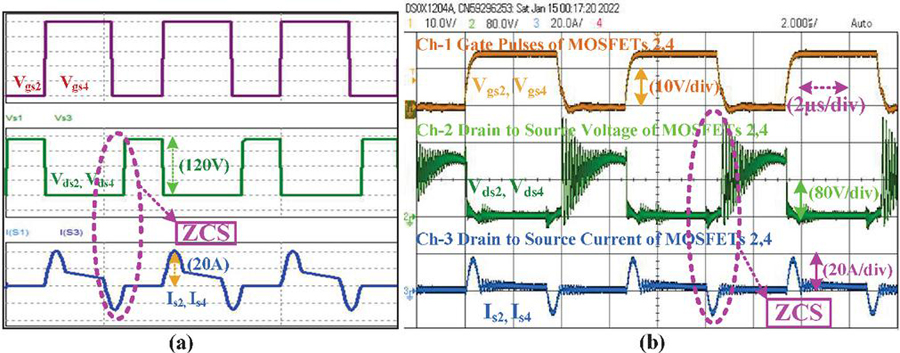
Figure 9 Standard waveforms obtained from (a) simulation and (b) Experimental results of gate signals, voltage stress, current through the pair of switches S, S at rated condition.
Figure 8 shows simulation and hardware results of gate signal (V, V), voltage stress (V, V), and currents (I, I) through the active switch pairs S, S. The simulation and experimental results of gate signal (V, V), voltage stress (V, V), and currents (I, I) through the switch pairs S, S are depicted in Figure 9. It is observed from Figures 8, 9 all the switches S to S are turned off with ZCS and denoted in a dotted circle. It helps the converter can operate at a higher frequency with lower switching losses. The voltage of the switches is settled at 120 V, and the peak current reaches 20 A during the shoot-through instant.
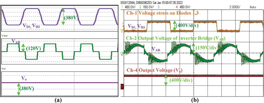
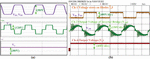
Figure 10 Standard waveforms obtained from (a) simulation and (b) Experimental results of diode voltage (V, V), inverter output (V), output voltage (V) at rated condition.
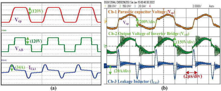
Figure 11 Standard waveforms obtained from (a) simulation and (b) Experimental results of parasitic capacitor voltage (V), inverter output voltage (V), Current through Leakage inductor (I) at rated condition.
Figure 10 shows the simulation and experimental results of voltage stress on rectifier diodes (V, V), output of inverter bridge voltage (V) and output voltage (V). The simulation and experimental results have observed that peak value of diode and output voltage is settled at 380 V. At the same time, the inverter output voltage (V) is settled at 120 V. In Figure 11, the voltage across the parasitic capacitor (V), the output of inverter bridge voltage (V) and current through the leakage inductor (I) are shown. The simulation and experimental results were observed that parasitic and inverter bridge voltage is settled at 120 V. When I reaches a peak value of 36 A, the same instant V voltage is zero.
The individual losses in each element are computed by using loss equations given in Table 3 and the parameters of selected components in the datasheet. The efficiency of the converter is obtained by using Equation (40) and associated total losses in the converter. Here, some of the efficiency model calculations are tabulated in Table 4.
| (40) |
Table 3 Losses equations used to compute losses in the converter
| Description | Equation |
| Gate driver losses | |
| Capacitor losses | |
| Switch conduction losses | |
| Turn on losses in the switch | |
| Total losses in rectifier diodes | |
| Total losses in the HFT | |
| Total losses in the inductor |
Table 4 Efficiency calculations of proposed converter
| Input Voltage | Parameter | 50 W | 150 W | 300 W |
| 40 V | Po | 47.425 | 145.642 | 290.92 |
| Losses | 1.513 | 4.137 | 9.104 | |
| Efficiency | 96.9 | 97.23 | 96.96 | |
| 48V | Po | 47.613 | 147.243 | 291.83 |
| Losses | 1.271 | 3.112 | 7.021 | |
| Efficiency | 97.39 | 97.93 | 97.65 | |
| 60V | Po | 48.512 | 147.431 | 292.967 |
| Losses | 1.005 | 2.425 | 6.192 | |
| Efficiency | 97.97 | 98.38 | 97.93 |
Were
C Switch input capacitor (F)
V Switch driving voltage (V)
f Switching frequency (Hz)
I Capacitor rms ripple current (A)
R Capacitor equivalent series resistor ()
I Switch rms current (A)
R Switch drain to source on-state resistance ()
C Switch output capacitor (F)
V Switch average voltage at turn off time (V)
V Diode forward voltage (V)
I Diode rms current (A)
I Diode average current (A)
R Diode turn on resistance ()
V Diode blocking voltage (V)
Q Diode reverse recovery charge
I rms current through transformer (A)
R Transformer DC resistance ()
P Core loss limit (mW/cm)
V Effective core volume (cm)
I rms current through transformer (A)
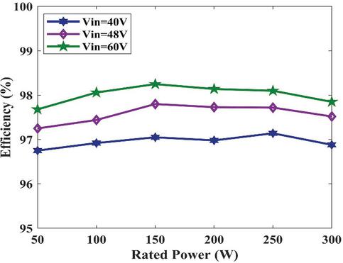
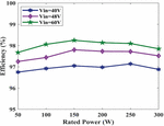
Figure 12 Efficiency of the proposed converter.
At 60 V rated power (300 W) the calculated efficiency of the converter is given below.
The mathematical efficiency calculation of converter is given in Table 4. The maximum efficiency of 98.38% is obtained for 60 V input at 150 W power. Minimum efficiency of 96.90% for 40 V input with 50 W power. In Figure 12 the measured efficiency of the converter is given. Here, the experimental efficiency values are slightly lesser then the mathematically calculated one. But both are very close, and the slight variation is due to the change in the resistance of the semiconductor while operating temperature changes.
5 Conclusion
A quasi-Y source magnetically coupled isolated partial resonant DC/DC converter is presented. By utilizing HFT parasitic components, LC parallel tank is formed, and soft switching (ZCS) occurs during the MOSFET turn-off instant. The mathematical and design methodology of the proposed converter is discussed. In addition, the simulation and experimental results are used to analyze the performance of the converter. Furthermore, coupled inductor and HFT provide a high voltage gain with less voltage stress on MOSFETs. Furthermore, it brings merits of ISC, and the soft switching feature improves the converter efficiency up to 98.38% at 60 V input voltage. The high gain, galvanic isolation and CIC feature of this converter are most suitable for renewable energy applications.
References
[1] O. Ellabban, H. Abu-Rub, and F. Blaabjerg, “Renewable energy resources: Current status, future prospects and their enabling technology,” Renew. Sustainable Energy Rev., vol. 39, pp. 748–776, 2014.
[2] Frede Blaabjerg and Dan M. Ionel “Renewable Energy Devices and Systems – State-of-the-Art Technology, Research and Development, Challenges and Future Trends”, Electric Power Components and Systems, 43:12, 2015, 1319–1328.
[3] S. Sathyan, H. M. Suryawanshi, M. S. Ballal and A. B. Shitole, “Soft-Switching DC–DC Converter for Distributed Energy Sources With High Step-Up Voltage Capability,” in IEEE Transactions on Industrial Electronics, vol. 62, no. 11, pp. 7039–7050, Nov. 2015.
[4] K.M. Smith and K. M. Smedley, “Properties and synthesis of passive lossless soft-switching PWM converters,” IEEE Transactions on Power Electronics, vol. 14, pp. 890–899, 1999.
[5] W. Li and X. He, “Review of Non-isolated High-Step-Up DC/DC Converters in Photovoltaic Grid-Connected Applications,” in IEEE Transactions on Industrial Electronics, vol. 58, no. 4, pp. 1239–1250, April 2011.
[6] M. Forouzesh, Y. P. Siwakoti, S. A. Gorji, F. Blaabjerg and B. Lehman, “Step-Up DC–DC Converters: A Comprehensive Review of Voltage-Boosting Techniques, Topologies, and Applications,” in IEEE Transactions on Power Electronics, vol. 32, no. 12, pp. 9143–9178, Dec. 2017.
[7] A. Mirzaee and J. S. Moghani, “Coupled Inductor-Based High Voltage Gain DC–DC Converter for Renewable Energy Applications,” in IEEE Transactions on Power Electronics, vol. 35, no. 7, pp. 7045–7057, July 2020.
[8] S. Hasanpour, Y. P. Siwakoti and F. Blaabjerg, “A New High Efficiency High Step-Up DC/DC Converter for Renewable Energy Applications,” in IEEE Transactions on Industrial Electronics, doi: 10.1109/TIE.2022.3161798.
[9] H. M. Suryawanshi et al., “Hybrid Control of High-Efficient Resonant Converter for Renewable Energy System,” in IEEE Transactions on Industrial Informatics, vol. 14, no. 5, pp. 1835–1845, May 2018.
[10] R. Chen, T. Liang, J. Chen, R. Lin and K. Tseng, “Study and Implementation of a Current-Fed Full-Bridge Boost DC-DC Converter With Zero-Current Switching for High-Voltage Applications,” in IEEE Transactions on Industry Applications, vol. 44, no. 4, pp. 1218–1226, July–Aug. 2008.
[11] A. B. Shitole, S. Sathyan, H. M. Suryawanshi, G. G. Talapur and P. Chaturvedi, “Soft-Switched High Voltage Gain Boost-Integrated Flyback Converter Interfaced Single-Phase Grid-Tied Inverter for SPV Integration,” in IEEE Transactions on Industry Applications, vol. 54, no. 1, pp. 482–493, Jan.–Feb. 2018.
[12] S. Tandon and A. K. Rathore, “Analysis and Design of Series LC Partial-Resonance-Pulse-Based ZCS Current-Fed Push-Pull Converter,” in IEEE Transactions on Industry Applications, vol. 57, no. 4, pp. 4232–4241, July–Aug. 2021.
[13] Fang Zheng Peng, “Z-source inverter,” in IEEE Transactions on Industry Applications, vol. 39, no. 2, pp. 504–510, March–April 2003.
[14] Y. P. Siwakoti, F. Z. Peng, F. Blaabjerg, P. C. Loh and G. E. Town, “Impedance-Source Networks for Electric Power Conversion Part I: A Topological Review,” in IEEE Transactions on Power Electronics, vol. 30, no. 2, pp. 699–716, Feb. 2015.
[15] A. Chub, D. Vinnikov, F. Blaabjerg and F. Z. Peng, “A Review of Galvanically Isolated Impedance-Source DC–DC Converters,” in IEEE Transactions on Power Electronics, vol. 31, no. 4, pp. 2808–2828, April 2016.
[16] Patidar, K., Umarikar, A.C.: ‘High step-up pulse-width modulation DC–DC converter based on quasi-Z-source topology’, IET Power Electron., 2015, 8, pp. 477–488.
[17] Y. P. Siwakoti, P. C. Loh, F. Blaabjerg, S. J. Andreasen and G. E. Town, “Y-Source Boost DC/DC Converter for Distributed Generation,” in IEEE Transactions on Industrial Electronics, vol. 62, no. 2, pp. 1059–1069, Feb. 2015.
[18] Y. P. Siwakoti, F. Blaabjerg and P. C. Loh, “Quasi Y-source boost DC–DC converter,” 2015 17th European Conference on Power Electronics and Applications (EPE’15 ECCE-Europe), 2015, pp. 1–10.
[19] J. Yuan, A. Mostaan, Y. Yang, Y. P. Siwakoti and F. Blaabjerg, “A Modified Y-Source DC–DC Converter With High Voltage-Gains and Low Switch Stresses,” in IEEE Transactions on Power Electronics, vol. 35, no. 8, pp. 7716–7720, Aug. 2020.
[20] Vinnikov, D., Roasto, I., Jalakas, T.: ‘New step-up DC/DC converter with high-frequency isolation’. Proc. 35th Annual Industrial Electronics Conf. (IECON), November 2009, pp. 670–675.
[21] N. Fakhri et al., “Optimization of Impedance-Source Galvanically Isolated DC-DC Converters with Reduced Number of Switches,” in IEEE Access, doi: 10.1109/ACCESS.2021.3139948.
[22] D. Vinnikov, I. Roasto, “Quasi-Z-source based DC/DC converters for distributed power generation,” IEEE Trans. Ind. Electron., vol. 58, no. 1, pp. 192–201, Jan. 2011.
[23] Siwakoti, Y.P., Blaabjerg, F., Loh, P.C., et al.: ‘High-voltage boost quasi-Z-source isolated DC/DC converter’, IET Power Electron., 2014, 7, pp. 2387–2395.
[24] Siwakoti, Y.P., Loh, P.C., Blaabjerg, F., et al.: ‘Magnetically coupled high-gain Y-source isolated DC/DC converter’, IET Power Electron., 2014, 7, pp. 2817–2824.
[25] M. Forouzesh and A. Baghramian, “Galvanically isolated high gain Ysource DC–DC converters for dispersed power generation,” in IET Power Electronics, vol. 9, no. 6, pp. 1192–1203, 18, 5, 2016.
[26] X. Ding, F. Wang, M. Zhou, Y. Cao, and Z. Wei, “Soft Switching High Voltage Gain Quasi-Z-Source DC-DC Converter with Switched-Capacitor Technique,” in IEEE Transactions on Industrial Electronics, doi: 10.1109/TIE.2021.3125649.
[27] Torki Harchegani, Amir, Amin Asghari, and Mostafa Jazaeri. “A new soft-switching multi-input quasi-Z-source converter for hybrid sources systems.” IET Renewable Power Generation 15.7 (2021): 1451–1468.
[28] H. Sugali and S. Sathyan, “Design and Analysis of Zero Current switching Y-Source DC/DC Converter for Renewable Energy Applications,” 2021 IEEE Kansas Power and Energy Conference (KPEC), 2021, pp. 1–5.
Biographies

Sugali Harinaik, received the B.Tech. degree in electrical and electronics engineering from the JNTUA College of Engineering Pulivendula, Andhrapradesh, India, in 2013 and the M.Tech. degree in integrated power systems from Visvesvaraya National Institute of Technology Nagpur, India, in 2017. He is currently working toward the Ph.D. degree in electrical and electronics engineering at National Institute of Technology, Tiruchirappalli, India.
His research interests include high gain DC/DC converters for renewable energy sources, soft switching, and impedance source DC/DC converters.

Shelas Sathyan, received the B.Tech. degree in electrical and electronics engineering from the Government College of Engineering Kannur, India, in 2009, and the M.Tech. and Ph.D. degrees in electrical engineering from the Visvesvaraya National Institute of Technology, Nagpur, India, in 2012 and 2017, respectively.
He is currently an Assistant Professor with the Department of electrical and electronics engineering at National Institute of Technology, Tiruchirappalli, India. His research interests include dc/dc converters, soft switching, DAB converters, and power factor correction.
Distributed Generation & Alternative Energy Journal, Vol. 38_2, 569–594.
doi: 10.13052/dgaej2156-3306.3829
© 2023 River Publishers