An LLC Resonant Half-Bridge Converter Optimal Design Using First Harmonic Approximation: A Complete Step-by-Design
G. Kiran Kumar and D. Elangovan*
School of Electrical Engineering, Vellore Institute of Technology, Vellore
Associate professor, TIFAC-CORE, Vellore Institute of Technology, Vellore
E-mail: kiran215vit@gmail.com, elangovan.devaraj@vit.ac.in
*Corresponding Author
Received 08 November 2021; Accepted 11 January 2022; Publication 27 February 2023
Abstract
There are several industrial uses for LLC resonant converters. The outcome of the converter is greatly influenced by the design and analysis methodologies used. An LLC resonant converter has been designed based on first harmonic approximation (FHA) modelling, and an optimal design technique has been provided in this work. The goal of this research is to provide a thorough design technique for an LLC resonant converter, based on rigorous quantitative analysis of the circuit’s steady-state performance. This study uses FHA technique, which greatly facilitates the model of the system, resulting in a linear circuit that can be analyzed using a standard complex ac-circuit analysis. The FHA methodology is used to establish circuit characteristics and to estimate the outcomes. Although half-bridge power converters are frequently employed in isolated, converters with high-voltage inputs, and medium-power applications are frequently constructed with resonant switching to increase efficiency, a feature that adds complexity but also provides various performance benefits. Two major benefits of the LLC resonant architecture are the soft-switching capabilities of the Power MOSFETs and secondary rectifiers, as well as the ability to operate at zero load. Additionally, the LLC resonant converter is simulated and the results are confirmed using PSIM.
Keywords: LLC resonant converter, first harmonic approximation (FHA), soft-switching, zero voltage switching, zero current switching.
1 Introduction
In power-supply designs and applications, efficiency, power density, and component density have all improved. This increased interest in resonant converters, particularly those with LLC resonant half-bridge converter (LLC-HBC) configurations, stems from the fact that these converters have the ability to switch at higher frequencies while experiencing lower switching losses [1–10]. There are several problems in developing these converters, including the fact that the LLC-HBC accomplishes power conversion with frequency modulation rather than pulse-width modulation, necessitating a different methodology [11, 12].
Designing of the LLC HBC is presented in this article, which begins with a brief review of the basic operating principles for resonance converters and an explanation of the energy-transfer function as a crucial constraint for the design procedure. Using voltage ratios and resonant circuit parameters, this energy transfer function describes the connection between output and input voltage. It is also known as a voltage-gain function. It is then explained how parameter values can be determined using this technique. To show how a design is created, an example of a 300 W output power converter with a 12 V output and 390 V input voltage is then presented in step-by-by-step process.
1.1 An Overview of Resonant Converters
In terms of topology, there are several different resonant-converter topologies. Using power switches, a square wave current or a voltage pulse is created and enforced to a resonant circuit [13]. The resonant circuit generates energy, some of which is tapped to power the output.
The parallel resonant converter (PRC) in Figure 1(a) and the series resonant converter (SRC) in Figure 1(b) are two common forms of resonant converters [14]. When the driving voltage frequency is changed, the resonant circuit’s impedance adjusts and the output voltage is regulated. This load and the impedance share the input voltage. The SRC DC gain is invariably less than 1, since it acts as a voltage divider between the load and the input [15]. When the load is light, the load’s impedance is much larger than the resonant circuit’s impedance, making it challenging to regulate the output since the frequency must access infinity as the load decreases. When the input voltage range is vast, even at minimal loads, a significant frequency change is needed to adjust the output.
Figure 1 Basic resonant converter topologies.
Figure 2 SPRC resonant configurations.
The load is linked in parallel with the resonant circuit in the PRC illustrated in Figure 1(a), necessitating a high quantity of circulating current. This makes parallel resonant topologies challenging to employ in situations with high power density or substantial load fluctuations [15].
1.2 Resonant Converters Topologies Based on LCC and LLC
To overcome these drawbacks, a converter known as a series-parallel resonant converter (SPRC) that associates both parallel and series topologies was proposed [16]. Figure 2(a) depicts an LCC setup, in which one inductor and two capacitors are used. As a result of the high AC currents, this design needs two separate physical capacitors, which are big and costly but solve the disadvantages of a single SRC or PRC by incorporating additional resonant frequencies [17–19]. The SPRC may be modified to produce an LLC resonant converter shown in Figure 2(b) using two inductors and one capacitor in order to achieve comparable properties without altering the physical component count. As compared to LCC topology, the series resonant (L) and transformer magnetizing inductances (L) of the LLC topology may frequently be combined into one physical part [20].
In comparison to traditional resonant converters, the LLC resonant converter offers several extra advantages. It may, for instance, maintain good efficiency while regulating the output through extensive load and line changes with a relatively little difference in switching frequency. Zero voltage switching (ZVS) and Zero current switching (ZCS) can be achieved across the full working range [21–25].
Table 1 Various resonant topologies comparison
| Parameter | LC Series | LC Parallel | LCC | LLC |
| ZVS/ZCS | ZVS | ZVS | ZVS | ZVS and ZCS |
| Frequency variation | Large | large | Narrow | Moderate |
| Component current/voltage stress | Lowest | High | Highest | Low |
Table 1 [26] shows the comparison between different resonant topologies. From the above table it is clear that the LLC topology has many benefits when compared to other resonant topologies. LLC topology has the benefit of both ZVS on primary side MOSFET switches and ZCS on the secondary side rectifier diodes. Thereby reducing the switching losses and enhance the converter efficiency. This topology has the additional benefits of moderate frequency variation for changing the output voltage and also the component voltage or current stress is low.
The rest of the paper is arranged as follows. Section 2 describes about the LLC HBC configuration, operation, modelling, and voltage-gain transfer function. ZVS constraints are described in Section 3. Section 4 discusses about the complete step-by-step design procedure of LLC HBC by taking an example. Section 5 describes the simulation results in all operating conditions and lastly conclusions are drawn in Section 6.
2 LLC HBC
There are four parts to this section: configuration, operation, circuit modelling with simplification, and the voltage-gain function. The configuration section covers the main components of the converter. The operation section covers a typical operating procedure and different modes of working of isolated LLC HBC. Circuit modelling describes the fundamental equations for the basis of voltage-gain function. The voltage-gain function serves as the foundation for the design process outlined in the next section.
2.1 Configuration
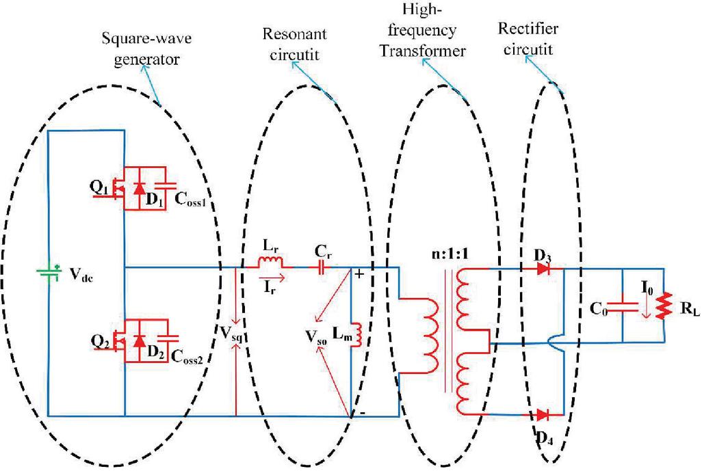
LLC HBC schematic is shown in Figure 3. In Figure 3, there are three major components: They are (1) Square wave generator, which generates a unipolar square wave by means of MOSFETS (2) Resonant circuit, formed by two inductors and one capacitor (3) an high frequency isolation transformer, transfers power from primary to secondary side (4) Rectifier circuit, formed by two diodes, to convert AC input into DC output.
Figure 3 Typical configuration of LLC HBC.
MOSFET power switches and are combined to create a square wave generator. and denotes the output capacitance of MOSFETs and and is considered to be a fixed. Switches and are driven with exchange of 50% duty cycles by this generator to produce a unipolar square-wave voltage, . In order to avoid cross conduction and to enable for ZVS to be accomplished, a short dead period is required between the successive transitions.
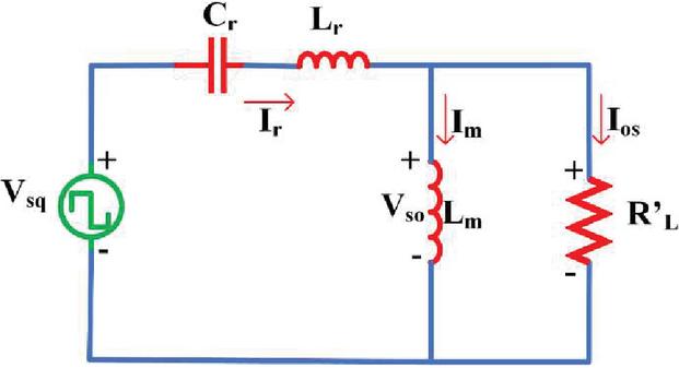
There are three components of a resonant circuit: series resonant inductor (), resonant capacitor (), and magnetizing inductor (). The transformer’s ratio of turns is given by the notation ‘n’. The electric current is transmitted by the resonant network, and as a consequence, energy is distributed and sent to the load via the transformer. The primary winding of the transformer is supplied by , a bipolar square wave voltage. To produce the appropriate output voltage, the primary side of the transformer takes this voltage and transfers it to the secondary side, where it is isolated electrically and has the required turns ratio. The load in Figure 4 comprises the load from Figure 3 as well as the losses from the transformer and output rectifiers.
Figure 4 Simplified converter circuit.
Two diodes form a full-wave rectifier on the converter’s secondary side, converting the AC input to DC output and powering the load . The rectified current and voltage are smoothed out by the output capacitor. A center tapped arrangement or a full-wave bridge with an output filter of capacitor can be used to build the rectifier network. Reducing conduction losses is particularly important in high-current and low-voltage situations where the rectifiers can be built using MOSFETs producing synchronous rectification.
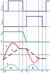
Figure 5 Operating waveforms of LLC HBC at resonance.
2.2 Operation
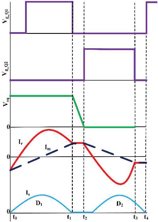
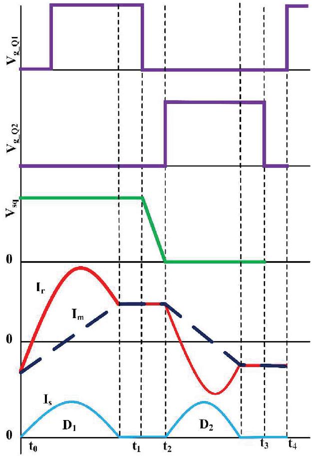
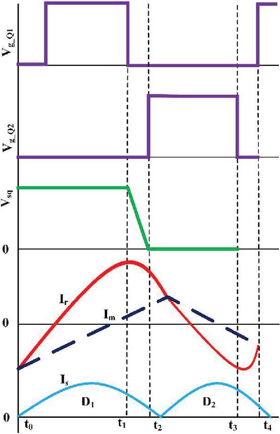
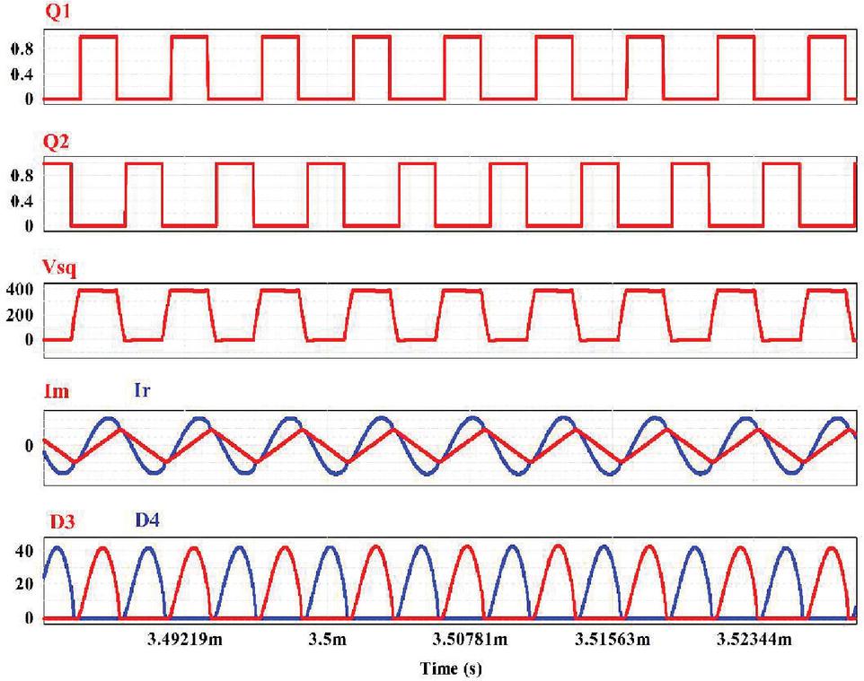
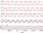
The connection between the series resonant frequency and the switching frequency , may be used to characterize the behavior of an LLC resonant converter. LLC HBC standard waveforms are illustrated at, below, and above the series resonant frequency are shown in Figures 5, 6, and 7 respectively. The graphs depicts the switch gate voltages of ), Q2(, the switch-node voltage (), the magnetizing current (), the resonant circuit’s current (I), and the diode current () on the secondary-side, from top to bottom. It is critical to understand that the sum of secondary-side current referred to the primary and the magnetizing current both combines and contributes the primary side current; however, the does not participate in the power transfer, since it flows only on primary side.
2.2.1 At resonance operation
The series resonant frequency and the switching frequency are the same in this operation. The I equals the , when switch is turned off, and then no power is transferred to the secondary side. To accomplish primary-side ZVS, the circuit delays the time at which switch is turned on. As a result, the secondary side rectifier diodes undergoes soft commutation. The sole point of action is apparent, while operating at series resonance. In order to accommodate input and output fluctuations, the switching frequency must be accustomed far from resonance.
Figure 6 Operating waveforms of LLC HBC in below resonance.
2.2.2 Below resonance operation
In this mode, the I has gone below the value before reaching the end of the driving pulse width, which would result in no further power transfer. Primary ZVS can still be achieved by operating below the series resonant frequency, as well as secondary-side soft commutation of the rectifier diodes. Therefore, extra circulating current is needed in the resonant circuit to supply the same quantity of energy to load as the secondary-side diodes operates in discontinuous current mode. As a result of the extra current, the conduction losses on the primary and secondary sides are increased. On the other hand, if the switching frequency drops too low, the primary ZVS may become ineffective. Correspondingly, there will be significant switching losses, as well as a number of related problems.
Figure 7 Operating waveforms of LLC HBC in above resonance.
2.2.3 Above resonance operation
There is a lesser circulating current on the primary side of the resonant circuit while operating in this mode. Since the resonant circuit current is in CCM, conduction losses are reduced, resulting in lower RMS current for the same load. When operating above the resonance frequency, it is still possible to produce primary ZVS even when the rectifier diodes are not soft-commutated. Under moderate-load conditions, operating above the resonance frequency might result in large frequency changes.
2.3 LLC SRC Modelling Using FHA
A voltage transfer function is required when designing a converter for output voltage control and variable energy transfer. The mathematical correlation between the input and output voltages is represented by this transfer function, which is also known as the output-to-input voltage gain. Gain formula development and gain features will be demonstrated in this section. FHA method, current commonly utilized in the construction of resonant converters.
The output-to-input voltage-transfer function can be developed using the FHA approach. The following are the first steps in the procedure:
• Do not include any higher-order harmonics in unipolar square wave current and voltage representation.
• Neglect the leakage inductance of the transformer and output capacitor
• Use the secondary-side variables that were acquired and refer to them on the primary side.
• Consider the bipolar square-wave voltage () as a reference for secondary voltage and current, and represent them using just their fundamental components, again disregarding any higher-order harmonics.
Figure 8 LLC resonant converter modelling.
After completing these procedures, the non-linear circuit model is shown in Figure 8(a) for the LLC HBC. In Figure 8(b), is the primary component of , whereas is the primary component of . The circuit in Figure 8(a), which is non-sinusoidal and nonlinear, is nearly changed into the circuit of Figure 8(b), which is linear and stimulates the resonant circuit by sinusoidal source, and drives an analogous resistive load shown in Figure 8(b). Because of and switching to produce the square wave voltage, the input voltage and output voltage are both sinusoidal with the same single frequency in this circuit model.
is a measure of the square-wave fundamental voltage on the input side and is given by
| (1) |
and the RMS value of this variable is given by
| (2) |
Due to the fact that is a square wave, the output fundamental voltage is
| (3) |
The phase difference between and is , its RMS voltage is given by
| (4) |
and are the primary components of current, and is given by
| (5) |
The phase difference between and is , its RMS output current is
| (6) |
The AC equivalent load resistance, , is then computed as follows:
| (7) |
The angular frequency given by
| (8) | ||
| (9) |
, , and , have inductive and capacitive reactance values of
| (10) | ||
| (11) | ||
| (12) |
The magnetizing current RMS value is given by
| (13) |
Series resonant circuit circulating current is given by
| (14) |
2.4 Voltage-Gain Function
The ratio or gain describes the correlation between the output and input voltages, which can be expressed as
| (15) |
To obtain Equation (15) as the ratio of the bipolar to unipolar square-wave voltage (), the DC output and input voltages are transformed into switching mode as explained previously:
| (16) |
Equation (16) may be used to estimate the AC voltage ratio, , by substituting and for and respectively.
| (17) |
Instead of , will be used in the notation to make things easier to read. To represent the connection between and , the electrical parameters , , and may be derived from Figure 8(b). As a result, the gain or voltage-transfer function from input to output will be
| (18) |
Where
2.4.1 Voltage-gain expression in normalisation format
To represent the voltage-gain function, we use absolute values in Equation (18). With such a structure, it is impossible to offer an overall overview of design difficulties. It is preferable to state it in a standard way. This may be accomplished by using the series resonant frequency () as a starting point for normalization. After that, we have the normalized frequency, which is written as
| (19) |
The following formula can be used to merge two inductances into one:
| (20) |
The series resonant circuit’s quality factor can be described as
| (21) |
These definitions allow us to normalize and describe the voltage gain function as
| (22) |
Equation (22) may be used to determine the connection in both the output and input voltages:
| (23) |
Where,
3 ZVS Constraints
The ability of the LLC converter topology to minimize switching losses considerably, largely via primary-side ZVS, is one of its key advantages. As a result of their soft-switching capabilities, resonant converters have a considerable advantage when it comes to switching over wide load areas. So, it’s important to comprehend the conditions for soft-switching, or more specifically ZVS. ZVS denotes that the switch obtains zero voltage earlier than being switched on. To achieve ZVS, we require a current to completely drain the MOSFET output capacitor energy before the MOSFET is turned on. To accomplish ZVS on MOSFETs in a switch network, three requirements must be met:
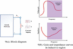
Figure 9 Block diagram of inductive impedance and gain and impedance curves in inductive region.
3.1 Inductive Input Impedance
In order to make the resonant tank inductive, we first require to guarantee a current is exists for the period of the turn-on transient, and that may be done by creating an inductive resonant tank. Figure 9(a) illustrates a case where the resonant tank is inductive, with current trailing, which results in the switch network output having a positive value when the circuit is first turned on. Resonant tanks with inductive components have a positive slope on their impedance curves and a negative slope on their gain curves, as seen in Figure 9(b).
3.2 Adequate Energy Storage in Resonant Tank
Inductive resonant tanks allow for charging or discharging of the MOSFET output capacitors by inductive current. It’s possible, however it doesn’t ensure ZVS because of inductor impedance. Additionally, we need to guarantee the inductor impedance exceeds the energy stored in the resonant tank’s MOSFET output capacitors, since this will ensure that the energy storage in MOSFET output capacitors is less than the resonant tank in switching circuit. The LLC-worst-case SRC’s scenario for attaining ZVS is
| (24) |
3.3 Adequate Dead-Time
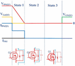
The resonant current is now capable of fully charging or discharging the MOSFET output capacitors, according to Equation (24). Consider the LLC-SRC half-bridge scenario in Figure 3. If a steady drain to source current is spent to discharge from the voltage to zero and charge from zero to , the time it takes for the charge or discharge operation to complete may be stated as .
| (25) |
ZVS cannot be obtained if the dead-time between and is shorter than . Conceptually, it may be demonstrated in Figure 10 as well.
3.4 Reasons for Not Using Capacitive Region
In the capacitive area, ZVS is impossible to accomplish, and as a result, switching losses are significant, minimizing the efficiency gains from employing an LLC converter. If operation is permitted in the capacitive area, many additional difficulties arise:
• Due to the loss of ZVS in this location, hard switching occurs on the primary side.
• To compensate for reverse-recovery losses due to capacitive current and hard switching on the primary side, MOSFET body diodes are typically slow-recovery types. When the MOSFETs’ reverse recovery is sluggish, it may allow for significant shoot-through, leading to excessive current and the failure of the MOSFETs.
• Large current peaks and Electromagnetic interference noise persist even though MOSFETs are designed to handle shoot-through current from reverse recovery.
Figure 10 Half-bridge LLC-SRC Switching transient.
4 Design Procedure
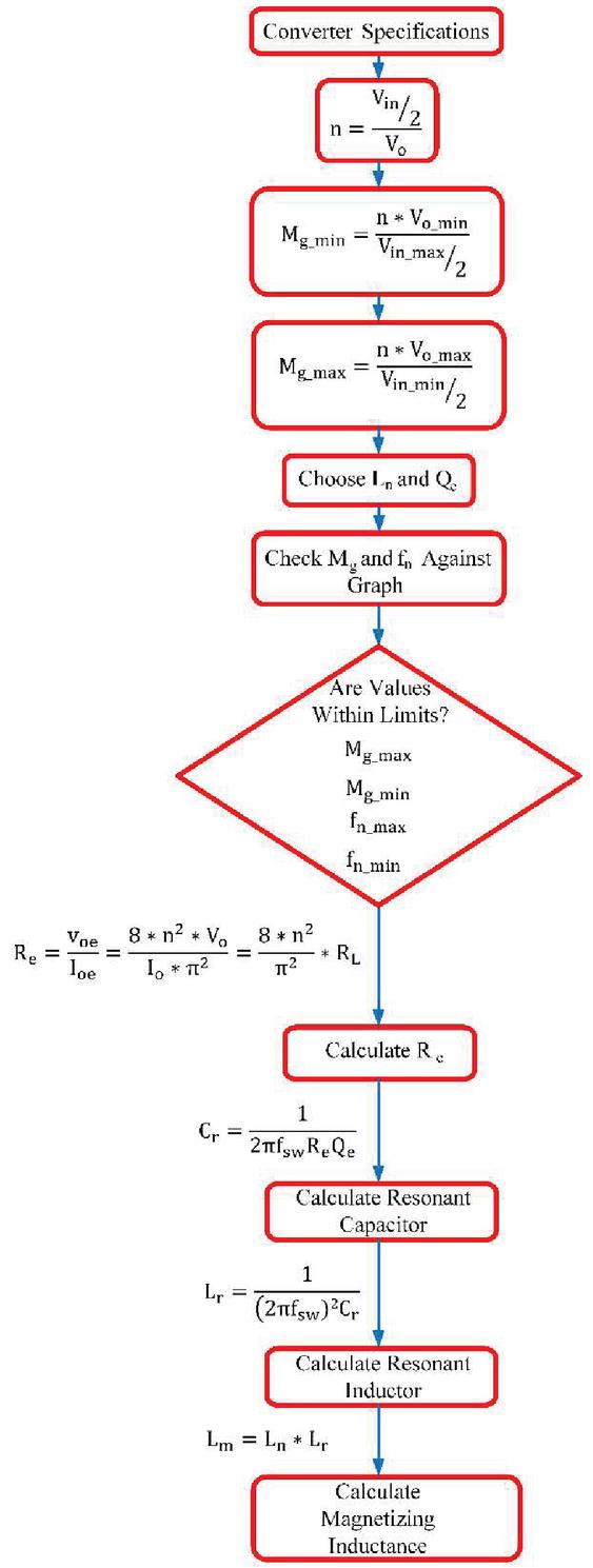
An LLC HBC design process is now provided, which is based on the analysis described thus far. The design flow diagram for the LLC resonant converter is shown in Figure 11. Table 2 describes the LLC HBC system specifications. The designed LLC resonant tank parameters are summarized in Table 3.
Figure 11 Design flow diagram of LLC HBC.
Table 2 LLC HBC system specifications
| Parameter | Value |
| Minimum Input Voltage (V) | 375 V |
| Rated Input Voltage (V) | 390 V |
| Maximum Input Voltage (V) | 410 V |
| Minimum output Voltage (V) | 12 V |
| Rated output Voltage (V) | 12 V |
| Maximum output Voltage (V) | 12 V |
| Rated output power (P) | 300 W |
| Resonant frequency | 200 kHz |
Table 3 Designed LLC resonant tank parameters
| Parameter | Value |
| 30.149 uH | |
| 21.004 nF | |
| 120.59 uH | |
| 120 kHz | |
| 240 kHz |
Step 1: Turns Ratio (n) Calculation of Transformer The following equation is used to estimate the transformer turns ratio:
Step 2: Compute the minimum and maximum gain
Step 3: Choose and As the required DC gain range is from 0.9365 to 1.024, so initially we will choose and .
Step 4: Calculate the load equivalent resistance
Step 5: Estimation of resonant circuit parameters
Step 6: Resonant circuit parameters Verification Series resonant frequency is given by
Inductance ratio
Quality factor
The frequency at minimum gain is maximum switching frequency which is given by
The frequency at maximum gain is minimum switching frequency which is given by
5 Simulation Results
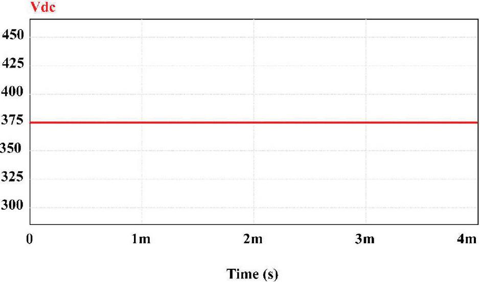
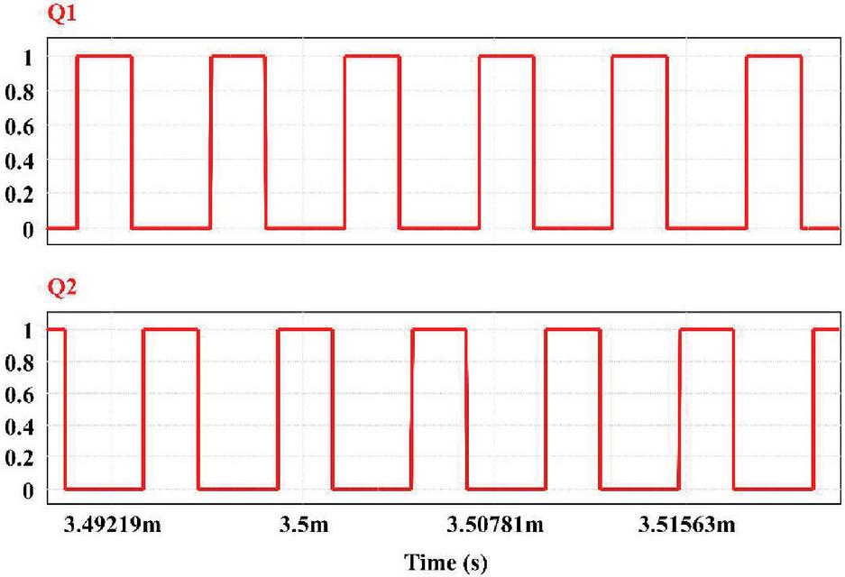
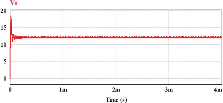
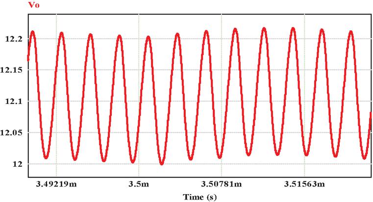
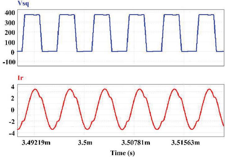
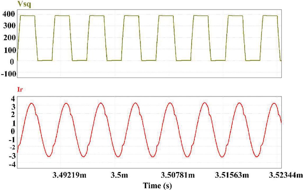
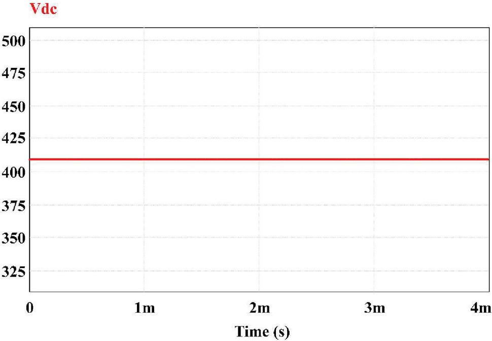
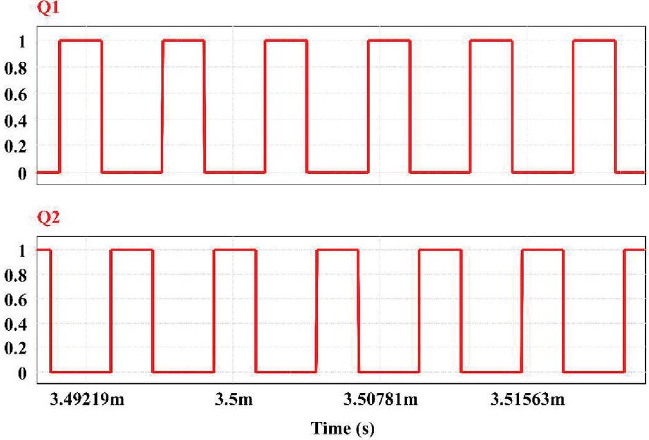
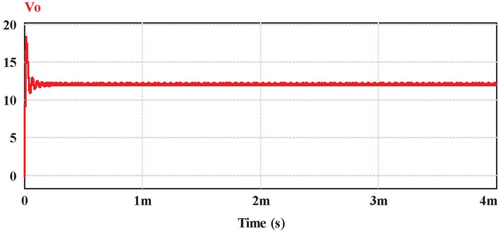
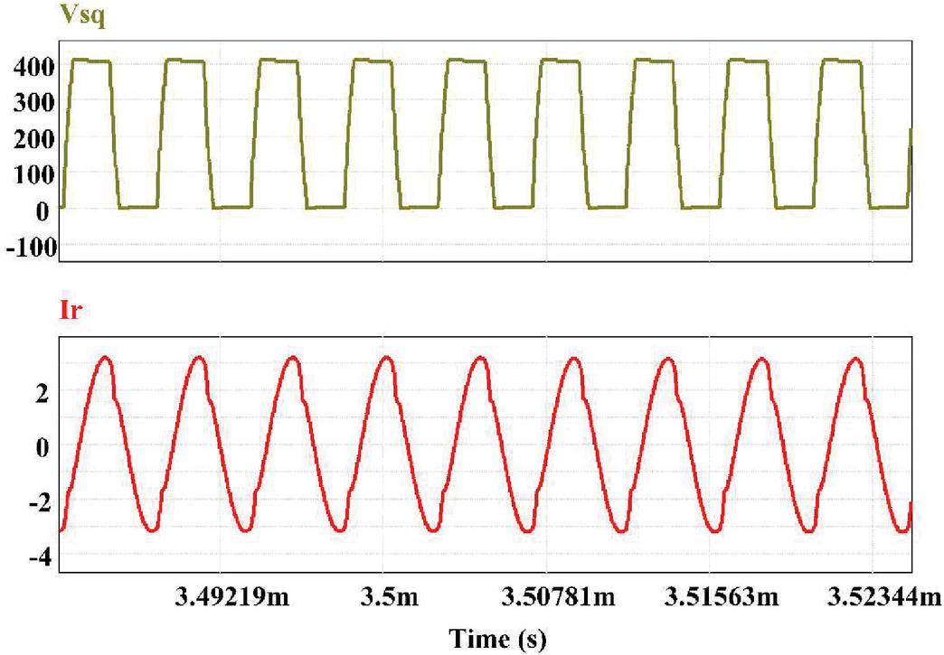
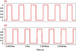
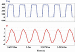
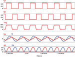
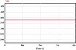
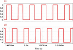
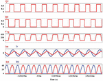
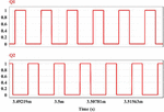
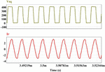
The minimum input voltage and the switching pulses applied to the LLC half-bridge converter at minimum input voltage (below resonance) with a delay time of 100 nano seconds is shown in Figures 12 and 13 respectively. The output voltage waveform and the zoomed output voltage regulating at 12 V is shown in Figures 14 and 15. Figure 16 shows the inverter voltage and series resonant current. The series resonant current is starting with a negative value and is lagging the inverter voltage, which means the converter operates in inductive region. As a result, the primary switches are operating in ZVS mode. Figure 17 shows the operating waveforms at below resonance. In this mode, the resonant current has gone below the magnetizing current value before reaching the end of the driving pulse width, which would result in no further power transfer. Therefore, operation below resonance is a discontinuous conduction mode since no current flows through the secondary diodes whenever I reaches I. Primary ZVS can still be achieved by operating below the series resonant frequency, as well as secondary-side soft commutation of the rectifier diodes.
5.1 At Minimum Voltage
Figure 12 Minimum input voltage applied to LLC HBC.
Figure 13 Pulses to switches Q and Q at minimum input voltage.
Figure 14 Output voltage at minimum voltage.
Figure 15 Zoomed output voltage regulating at minimum voltage.
Figure 16 Inverter voltage and series resonant current at minimum input voltage.
Figure 17 Operating waveforms at below resonance.
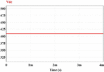
Figure 18 Rated input voltage applied to LLC HBC.
Figure 19 Pulses to switches Q and Q at rated input voltage.
Figure 20 Output voltage at rated voltage.
5.2 At Rated Voltage
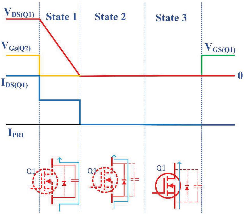
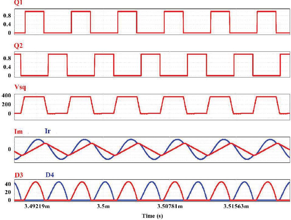
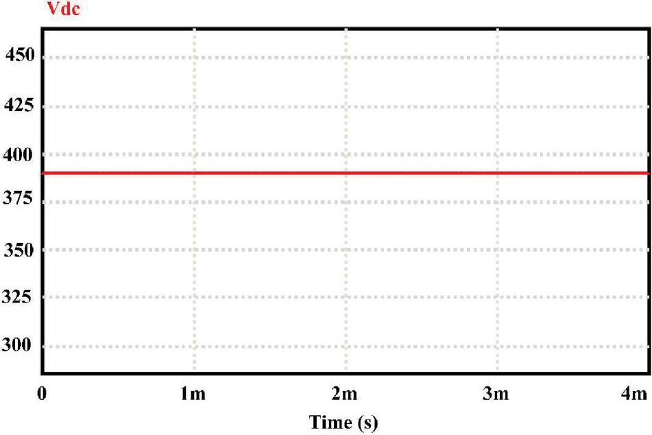
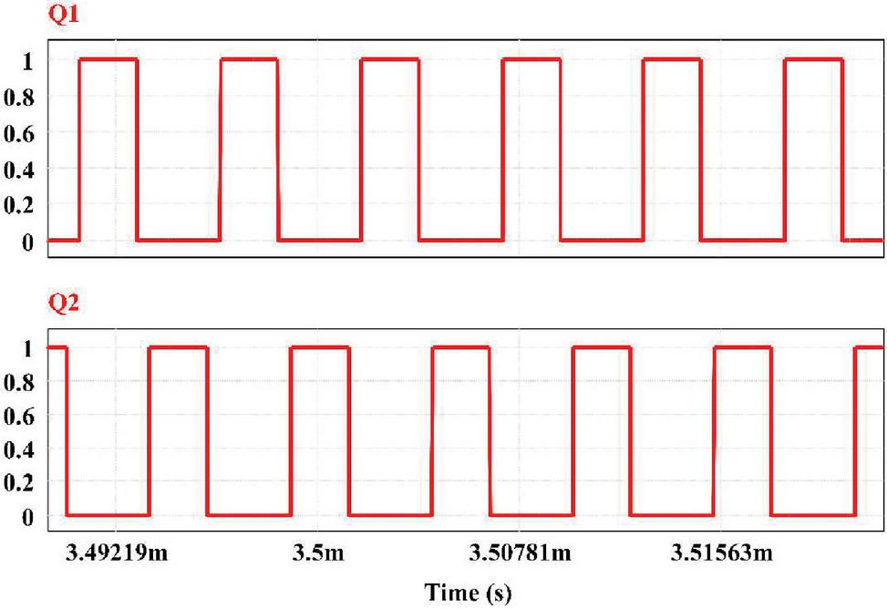
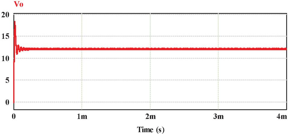
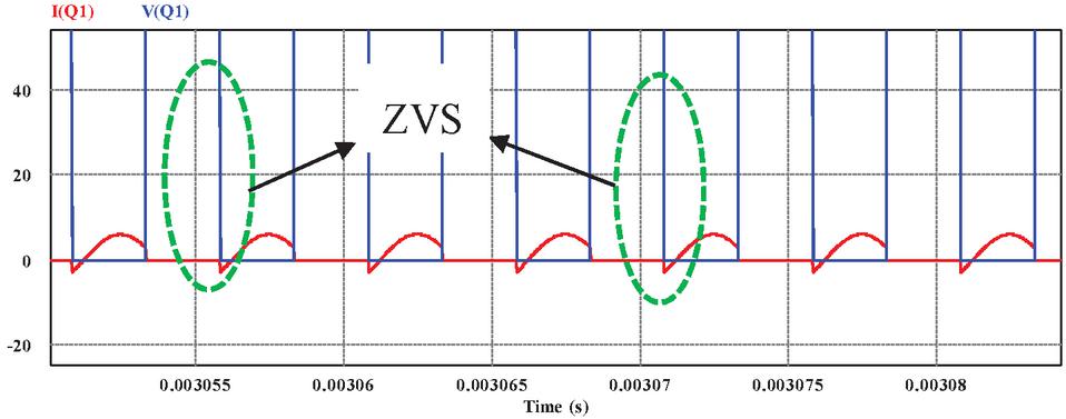
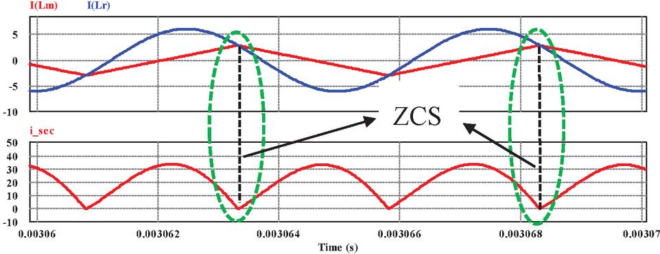
The rated input voltage and the switching pulses applied to the converter at nominal input voltage (at resonance) with a delay time of 100 nano seconds is shown in Figures 18 and 19 respectively. The output voltage waveform regulating at 12 V is shown in Figure 20. Figure 21 shows the inverter voltage and series resonant current. The series resonant current is starting with a negative value and is lagging the inverter voltage, which means the converter operates in inductive region. As a result, the primary switches are operating in ZVS mode. ZVS can also be understood with the help of switch drain current and switch gate voltage as shown in Figure 22. ZCS operation is shown in Figure 23. The I equals the , when switch is turned off, and then no power is transferred to the secondary side. To accomplish primary-side ZVS, the circuit delays the time at which switch is turned on. As a result, the secondary side rectifier diodes undergo soft commutation.
Figure 21 Inverter voltage and series resonant current at rated input voltage.
Figure 22 ZVS operation simulation waveform.
Figure 23 ZCS operation simulation waveform.
Figure 24 Operating waveforms at resonance.
Figure 25 Maximum input voltage applied to LLC HBC.
Figure 26 Pulses to switches Q and Q at maximum input voltage.
5.3 At Maximum Voltage
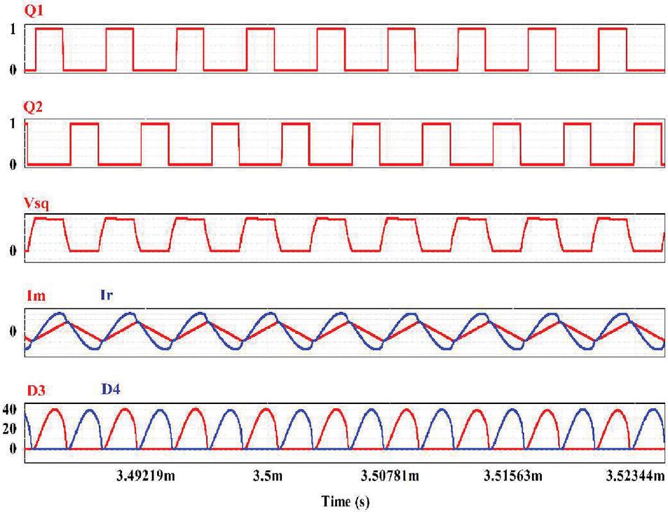
The maximum input voltage and the switching pulses applied to the converter at maximum input voltage (at above resonance) with a delay time of 100 nano seconds is shown in Figures 25 and 26 respectively. The output voltage waveform regulating at 12 V is shown in Figure 27. Figure 28 shows the inverter voltage and series resonant current. The series resonant current is starting with a negative value and is lagging the inverter voltage, which means the converter operates in inductive region. As a result, the primary switches are operating in ZVS mode. Figure 29 shows the operating waveforms at above resonance.
Figure 27 Output voltage at maximum voltage.
Figure 28 Inverter voltage and series resonant current at maximum input voltage.
Figure 29 Operating waveforms at above resonance.
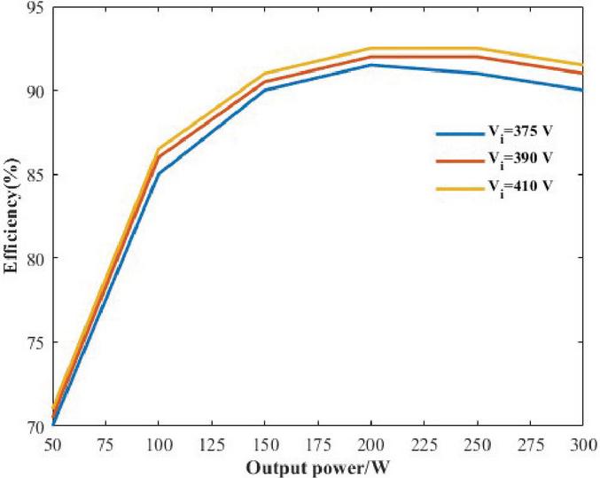
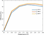
Figure 30 Efficiency curves.
The system efficiency curves for various input voltages and output power is shown in Figure 30. Harmonics and conduction losses are reduced are reduced when the input voltage is increased, resulting in increasing the efficiency. The maximum efficiency at 200 W is about 92.58%.
6 Conclusion
This article has covered all the bases when it comes to developing an isolated LLC resonant half-bridge converter. Various resonant topologies are compared based on different parameters in Table 1. Among all the resonant topologies LLC is the best one because it can achieve ZVS on primary side and ZCS on secondary side. Due to these switching losses can greatly reduce. The LLC converter has been analyzed in all the three modes i.e at resonance, below resonance and above resonance operating conditions. Thus, a straightforward but precise design-oriented model and an easy step-by-step design technique have been developed, ensuring stable operation at full load, ZVS under all operational situations. To begin a novel design of this kind, the FHA technique has proven very beneficial. It has also been demonstrated how to apply this strategy through a step-by-step design example.
References
[1] Y. Tran, F. D. Freijedo, and D. Dujic, “Open-loop power sharing characteristic of a three-port resonant LLC converter,” CPSS Trans. Power Electron. Appl., vol. 4, no. 2, pp. 171–179, Jun. 2019.
[2] Y. Wei, N. Altin, Q. Luo, and A. Nasiri, “A high efficiency, decoupled on-board battery charger with magnetic control,” in Proc. 7th Int. Conf. Renewable Energy Res. Appl., 2018, pp. 920–925.
[3] B. Yang, F. C. Lee, A. J. Zhang, and G. Huang, “LLC resonant converter for front end DC/DC conversion,” in Proc. 17th Annu. IEEE Appl. Power Electron. Conf. Expo., 2002, pp. 1108–1112.
[4] Y. Wei, Q. Luo, J. M. Alonso, and A. H. Mantooth, “A magnetically controlled single-stage AC/DC converter,” IEEE Trans. Power Electron., vol. 35, no. 9, pp. 8872–8877, Sep. 2020.
[5] S. Chen et al., “Research on topology of the high step-up boost converter with coupled inductor,” IEEE Trans. Power Electron., vol. 34, no. 11, pp. 10733–10745, Nov. 2019.
[6] Y. Wei, Q. Luo, Z. Wang, L. Wang, J. Wang, and J. Chen, “Design of LLC resonant converter with magnetic control for LEV application,” in Proc. IEEE 10th Int. Symp. Power Electron. Distrib. Gener. Syst., 2019, pp. 854–859.
[7] Y. Wei, Q. Luo, and A. Mantooth, “Comprehensive analysis and design of LLC resonant converter with magnetic control,” CPSS Trans. Power Electron. Appl., vol. 4, no. 4, pp. 265–275, Dec. 2019.
[8] Y. Shen, W. Zhao, Z. Chen, and C. Cai, “Full-bridge LLC resonant converter with series-parallel connected transformers for electric vehicle on-board charger,” IEEE Access, vol. 6, pp. 13490–13500, 2018.
[9] C. Hua, Y. Fang, and C. Lin, “LLC resonant converter for electric vehicle battery chargers,” IET Power Electron., vol. 9, no. 12, pp. 2369–2376, Oct. 2016.
[10] H.-D. Gui, Z. Zhang, X.-F. He, and Y.-F. Liu, “A high voltage-gain LLC micro-converter with high efficiency in wide input range for PV applications,” in Proc. IEEE Appl. Power Electron. Conf. Expo., 2014, pp. 637–642.
[11] Y. Wei, Q. Luo, and A. H. Mantooth, “Overview of modulation strategies for LLC resonant converter,” IEEE Trans. Power Electron., vol. 35, no. 10, pp. 10423–10443, Oct. 2020.
[12] Y. Wei, Q. Luo, X. Du, N. Altin, A. Nasiri, and J.M. Alonso, “A dual half bridge LLC resonant converter with magnetic control for battery charger application,” IEEE Trans. Power Electron., vol. 35, no. 2, pp. 2196–2207, Feb. 2020.
[13] Yu, S. Y. and Kwasinski, A., “Realization and comparison of a new push-pull direct connected multiple-input converter family for distributed generation applications,” Proc. INTELEC, pp. 1–8, 2011.
[14] Yang, B., Lee, F. C., Zhang, A. J. and Huang, G., “LLC resonant converter for front end DC/DC conversion,” Proc. APEC, pp. 1108–1112, 2002.
[15] Huang, D., Lee, F. C. and Fu, D., “Classification and selection methodology for multi-element resonant converters,” Proc. APEC, pp. 558–565, 2011.
[16] I. Batarseh, “Resonant Converter Topologies with Three and Four Energy Storage Elements”, IEEE Transactions on Power Electronics 9, vol. 1, 1994, pp. 64–73.
[17] R. L. Steigerwald, “A Comparison of Half-Bridge Resonant Converter Topologies,” IEEE Transactions on Power Electronics 3, vol. 2, 1988, pp. 174–182.
[18] A. Pawellek, A. Bucher, T. Duerbaum, “Analysis and Design of a Resonant LCC Converter for Low Profil Applications” Energy Conversion Congress and Exposition (ECCE), 2010, pp. 3333.
[19] Huang, Hong. “FHA-based voltage gain function with harmonic compensation for LLC resonant converter.” In 2010 Twenty-Fifth Annual IEEE Applied Power Electronics Conference and Exposition (APEC), pp. 1770–1777. IEEE, 2010.
[20] C. Oeder, “Analysis and Design of a Low-Profile LLC Converter”, IEEE international Symposium on Industrial Electronics, Bari, Italy, 2010, pp. 3859–3864.
[21] Wei, Yuqi, Quanming Luo, Zhiqing Wang, and Homer Alan Mantooth. “A complete step-by-step optimal design for LLC resonant converter.” IEEE Transactions on Power Electronics 36, no. 4 (2020): 3674–3691.
[22] R. Beiranvand, B. Rashidian, M. R. Zolghadri, and S. M. H. Alavi, “A design procedure for optimizing the LLC resonant converter as a wide output range voltage source,” IEEE Trans. Power Electron., vol. 27, no. 8, pp. 3749–3763, Aug. 2012.
[23] Z. Fang, S. Duan, C. Chen, X. Chen, and J. Zhang, “Optimal design method for LLC resonant converter with wide range output voltage,” in Proc. IEEE Appl. Power Electron. Conf. Expo., Long Beach, CA, Mar. 2013, pp. 2108–2109.
[24] R. Yu, G. K. Y. Ho, B. M. H. Pong, B. W. K. Ling, and J. Lam, “Computeraided design and optimization of high-efficiency LLC series resonant converter,” IEEE Trans. Power Electron., vol. 27, no. 7, pp. 3243–3256, Jul. 2012.
[25] X. Fang et al., “Efficiency-oriented optimal design of the LLC resonant converter based on peak gain placement,” IEEE Trans. Power Electron., vol. 28, no. 5, pp. 2285–2296, May 2013.
[26] Texas Instruments, “Survey of resonant converter topologies” http://www.ti.com
Biographies

G. Kiran Kumar received the B.Tech degree in Electrical and Electronics Engineering from Jawaharlal Nehru Technological University, Anantapur, India and M.Tech Degree in Power Electronics and Drives from Vellore Institute of Technology, Vellore, India. He is perusing Ph.D. degree in Power Electronics in the School of Electrical Engineering, Vellore Institute of Technology, and Vellore, India. His current research interest includes high efficiency and high frequency switch mode power supply, fault-diagnosis, and fault-tolerant DC-DC converters for HEV.

D. Elangovan is an associate professor of Energy and power electronics department in School of Electrical Engineering, and also the deputy director of TIFAC-CORE, Vellore Institute of Technology, Vellore, India. He received the Ph.D. degree in Power Electronics and working as Associate Professor in School of Electrical Engineering, VIT, and Vellore, India. He has published more than 70 peer-reviewed journals and conference papers. His current research interests include wireless power transfer, modelling and controlling of DC-DC power converters, fault-diagnosis, and fault-tolerant DC-DC converters for HEV.
Distributed Generation & Alternative Energy Journal, Vol. 38_3, 841–874.
doi: 10.13052/dgaej2156-3306.3836
© 2023 River Publishers


