Dual Inductor Based Two Input Two Output DC-DC Converter and its Analysis for DC Microgrid Application
R. Aravind1, Sivaprasad Athikkal2,*, Ravi Eswar Kodumur Meesala1, K. Jyotheeshwara Reddy3, Ritesh Dash3 and Vivekanandan Subburaj3
1Department of EEE, SRM IST, Kattankulathur, India
2Department of EEE, Muthoot Institute of Technology and Science, Ernakulam, India
3School of EEE, Reva University, Bangalore, India
E-mail: sivanuday@gmail.com
*Corresponding Author
Received 31 January 2022; Accepted 26 April 2022; Publication 27 February 2023
Abstract
Two input two output DC-DC converters with two switched inductor structure are widespread in DC micro grid and Electric Vehicle (EV) applications with merits of solid structure, lower cost and high-power density. However, owing to the low voltage levels of the non-conventional sources used in the above applications, the significance of step up type DC-DC converters is so high. In this paper, a step up converter that is expert to deliver two different voltages at the output side from two different input energy sources is proposed as a new topology. It mainly contains two inductors for improving the voltage conversion ratio. Thorough analysis of converter has been performed with support of necessary equations and circuits. The performance assessment of DC-DC converter is done with simulation and experimental platforms and required waveforms are presented. A comparative study of the proposed converter is also fulfilled to signify the better features of the converter.
Keywords: Dual inductor based converter, multiport boost type DC-DC converter, theoretical analysis, microgrid/EV applications.
1 Introduction
In the existing situation, the usage of non-conventional sources has been radically boosted especially in the areas of DC microgrid, electric vehicle, fuel cell, etc. However, most of power converter interfaces have poor voltage profile. Hence the selection of suitable converter interface based on the application is highly important to realize efficient integration of various sources. A Two switch based boost converter for fuel cell powered vehicle application that has high gain relation has been discussed in [1]. A positive voltage two input two output converter that outshines the drawback of typical buck-boost converter with two inputs is presented in [2]. The creation of MIMO (Multi Input Multi Output) converters are proposed in [3] with low cost and simple structure. But most of the converters have the demerits of higher voltage and current stress on the switching devices and constrains on load currents and output voltages. In [4], various MIMO topologies that are operated in step up, step down operations are derived and analysed. However, thorough investigations on a particular topology is missing. A novel multi-port converter that has a single inductor structure is proposed in [5]. However, the number of power switches are high in the given converter that may increase the overall intricacy. A new concept of high boost multiport converter is narrated in [6] with capacitor-diode based voltage boosting cell. Even though the converter offers better voltage gain, the count of passive components and power switches are increased with the quantity of input sources that affects the system efficiency. Detailed analysis of various integrated multiport converters is presented in [7]. Various design equations are described for the investigation of each of the presented topologies. A single inductor based MIMO converter with double conversion elimination method is introduced in [8]. This method is used to achieve a reduction in double converted power by a significant amount. A two inductor based two input converter is introduced in [9]. It has compact structure and better voltage conversion ratio. However, the number of conducting devices are relatively high that may affect the loss values. A novel multi input high gain converter for cancelling ripples from input and to enhance the consumer’s safety on load side along with high power density and efficiency is introduced in [10]. However, the presence of more number of coupled inductors and other components increases the overall circuit complexity and cost.
An overall overview and global picture of step up type converters to demonstrate the present relevance of high voltage gain in various applications are described in [11]. A boost type three input dual output converter and the theoretical studies are presented in [12]. In [13], a MIMO converter with a single inductor with detailed analysis is presented. Here, the two outputs and inputs can be easily removed and added deprived of altering the control strategy. The inputs and outputs are connected in series and are independent to each other. However, one of the source side switches is need to be turned on permanently to realize better voltage conversion ratio. This increases the overall losses of the converter. A multiport converter for EV application is narrated in [14]. The number of conduction devices is more in each working states of the converter that causes high conduction losses in the given converter. A non-isolated four port converter with the capability of bidirectional energy flow to charge the battery between diversified energy supplies is presented in [15]. However, more number of conducting devices in each working state causes high losses in the system.
A comprehensive review of various multiport converters used for renewable energy integration is described in [16]. The review investigates both isolated and non-isolated topologies in an elaborated manner. To elucidate the problem of hard switching operation, a three port soft switched converter is implemented in [17] with power flow to energy storage device from the output. However, the presence of auxiliary circuit increases the converter complexity. A novel multi input power converter has been explored in [18]. But it contains larger number of switches and storage elements that affects the overall converter efficiency and operation. A two input converter and the implementation of a closed loop control scheme for the converter is detailed in [19] with the explanation of output voltage regulation. A novel modified two input converter has been proposed in [20]. The converter analysis are presented with the support of experimental results. But the voltage gain of the converter is reasonably lesser. Henceforth, in this paper a novel two input two output dual inductor based converter is presented. The converter has
• Good voltage gain compared to typical boost converter
• Lesser voltage stress through the switching components
• Flexibility in the duty ratios to achieve better voltage gain
• Energy deposited in the inductor can be distributed to the load without any additional clamping circuit.
• Capability to incorporate two dissimilar voltage-current characteristic sources
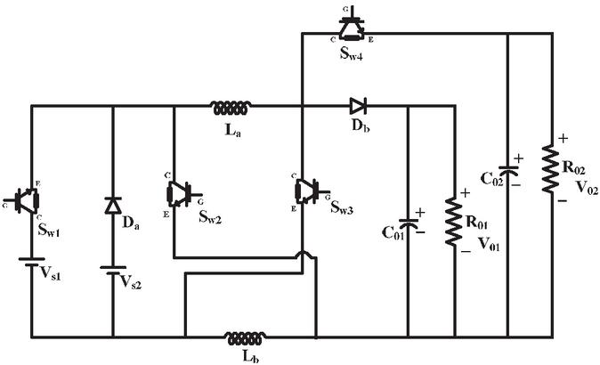
Figure 1 Proposed converter circuit diagram.
2 Circuit Diagram
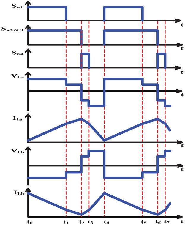
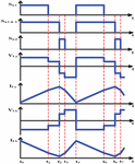
The circuit representation of two input two output two switched inductor converter is illustrated in Figure 1. The count of power switches is four, the count of diodes and inductors are two as shown in the circuit and the total count of capacitors are also two. The duty ratios of the switching pulses are selected as shown in Figure 2. Here the inductor operation is considered only in continuous conduction mode (CCM) even though it may operate in discontinuous mode based on the sources.
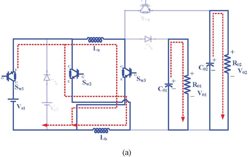
2.1 Mode I
The mode I operation circuit is given in Figure 3(a). Initially the input voltage V charge the inductors L and L through the switches S and S, hence inductor current is linearly rising. The output capacitor C and C have been discharged at the same time to ensure the continuous supply to the load.
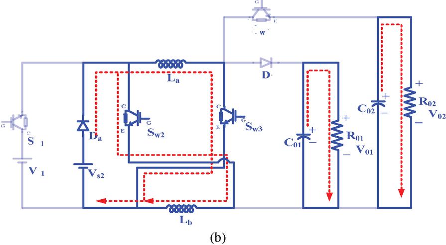
2.2 Mode II
The circuit in mode II is displayed in Figure 3(b), here the input voltage V is used to charge the inductors L and L through the switches S and S.
Hence the inductor current is linearly rising. The output capacitor C and C have been discharged at the same time to supply the loads.
Figure 2 Analytical waveform for the proposed converter.
Figure 3 Continued
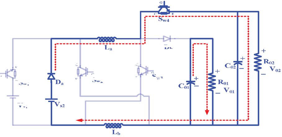
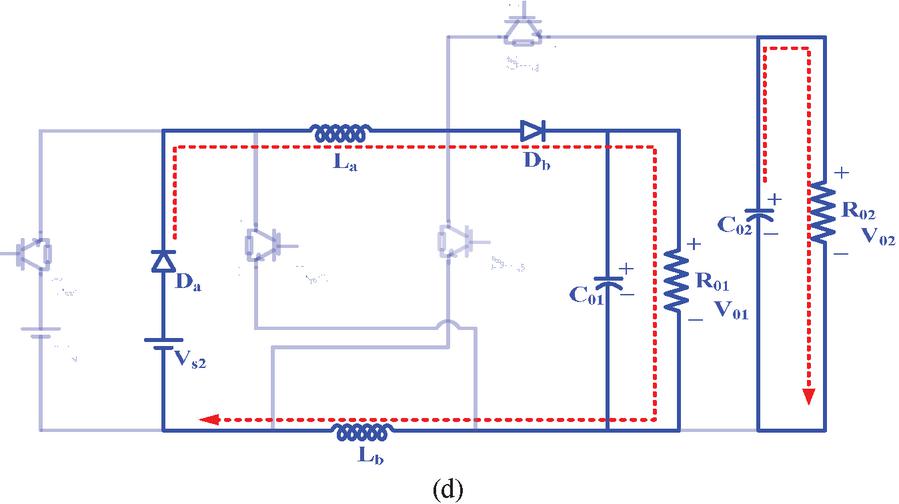
Figure 3 The corresponding circuits for different operating modes (a) mode I (b) mode II (c) mode III (d) mode IV.
2.3 Mode III
The circuit of mode III operation is illustrated in Figure 3(c). Here the input voltage V gives the continuous supply to the load through the inductor L, switch S and energizes the capacitor C. Still the output capacitor C is used to supply the load by de-energizing its stored energy.
2.4 Mode IV
The circuit in mode IV is revealed in Figure 3(d). Here V is the input voltage that gives the supply to the load R through the inductor L, diode D and also energizes the capacitor C. At the same time output capacitor C dissipates its stored energy to deliver energy to the load R.
3 Analysis of a Converter
The necessary equations of the converter in various working modes have been derived and presented in this session.
In mode I, voltages across the inductors are
| (1) | ||
| (2) |
In this mode, the switch voltages of S, S, S and S and diode voltages of D and D are extracted as
| (3) | |
| (4) | |
| (5) | |
| (6) |
In mode II, voltages across the inductors are
| (7) | |
| (8) |
In this mode, the switch voltages of S, S, S and S and diode voltages of D and D are extracted as
| (9) | |
| (10) | |
| (11) | |
| (12) | |
| (13) |
In mode III, voltages across the inductors are
| (14) | ||
| (15) |
In this mode, the switch voltages of S, S, S and S and diode voltages of D and D are extracted as
| (16) | |
| (17) | |
| (18) | |
| (19) | |
| (20) |
In mode IV, voltages across the inductors are
| (21) | ||
| (22) |
In this mode, the switch voltages of S, S, S and S and diode voltages of D and D are extracted as
| (23) | |
| (24) | |
| (25) | |
| (26) |
Table 1 Simulation/experimental parameters
| Simulation Parameters | ||
| S. No | Parameters | Specification |
| 1. | Input Voltages (V, V) | 24 V, 12 V |
| 2. | Inductor (L & L) | 5 mH |
| 3. | Switching Frequency (f) | 20 kHz |
| 4. | Duty ratio (D, D, D, D) | 50%, 70%, 70%, 10% |
| 5. | Output Capacitor (C, C) | 47 F |
| 6. | Output Voltages (V, V) | 118 V, 60 V |
| 7. | Load Resistors (R, R) | 100 |
4 Simulation/Experimental Results
4.1 Simulation Results
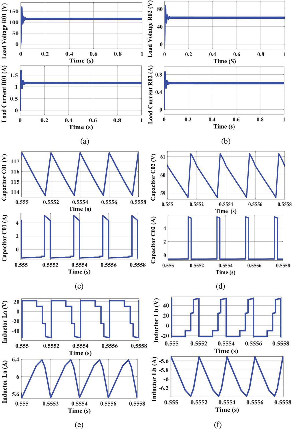
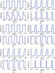
In the Simulink/MATLAB platform, the simulation analysis of the introduced converter is done. The parameter values for the simulation/experimental analysis are listed in the Table 1. The working of the inductor is in continuous conduction mode and waveforms generated in the software simulation like voltage and current of inductors, capacitors, load, etc, are displayed in Figure 4. The simulation waveforms for the load currents and voltages across R and R are shown in the Figure 4(a & b). The voltages across the loads R and R are 118 V and 60 V correspondingly for the given converter and the respective output load current values are 1.3 A and 0.7 A. The capacitor current and voltage waveforms are revealed in Figure 4(c & d). The voltage across C and C are 118 V and 60 V correspondingly for the given converter with a maximum ripple content of 3 V across them. Here one of the output voltage is considered as 118 V since it is a standard DC microgrid specification.
Figure 4 Simulation results (a) load voltage and current through R (b) load voltage and current through R (c) voltage and current through C (d) voltage and current through C (e) voltage and current across L (f) voltage and current across L.
During the first three modes of operation capacitor C is used to discharge the energy to the load R and in fourth mode of operation, the capacitor C is charged through the diodes D, D and Inductor L from the input source V. During first two modes and the fourth mode of operation capacitor C is used to discharge the energy to the load R and in the third operating mode, the capacitor C is getting charged through the diode D, inductor L and switch S from the input sources V. The respective average current values of the capacitors C and C are 5 A. The inductor current and voltage waveforms obtained from the simulation circuit are shown in the Figure 4(e & f). The voltage across L is charged with 24 V and 12 V in first two working modes and de-energized with the voltage of 24 V and 50 V correspondingly in the final two working modes. At the same time inductor L is charged with negative polarity (i.e., 24 V and 12 V) in first two working modes and de-energized with the voltage of 24 V and 50 V respectively (due to the position of inductor L in the circuit) in the final modes of operations and the corresponding average current for the both inductors L and L are 6 A. Here 0.8 A is the ripple content in inductor current and 3 V is the ripple content in capacitor voltage.
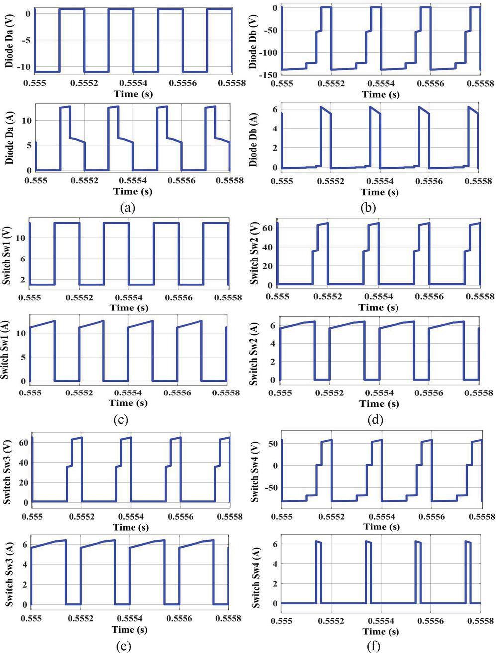
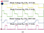
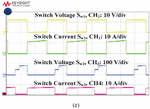
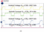
The simulation waveforms for the diode voltage and currents across the D and D are revealed in Figure 5(a & b). The voltage across the Diode D is 12 V (i.e., V–V) for the first mode of operation and in the other three modes, the diode D is in ON state, hence the voltage is zero. Also, the voltage across the diode D is 148 V, 120 V and 50 V for the first three modes of operations and in fourth mode diode D is in ON state, hence the voltage is zero. The respective average currents through both diodes are 8 A. The simulation waveforms for the switch voltages and currents are shown in Figure 5(c–f). The voltage across S and S are 62 V (Figure 5(d&e)) in last two working modes. In last three working modes, the voltage stress across S (Figure 5(c)) is observed as 12 V (i.e., (i.e., V–V) and the voltage across the switch S (Figure 5(f)) is observed as 82 V (V–(V V)) in mode I, 70 V (V–(V V)) in mode II, 58 V(V–V) in mode IV. In mode III, since the switch is conducting, the voltage stress is zero. The average current following through all the switches are 6 A.
Figure 5 Voltage and current waveforms obtained from simulation analysis (a) for D (b) for D (c) for S (d) for S (e) for S (f) for S.
4.2 Experimental Results
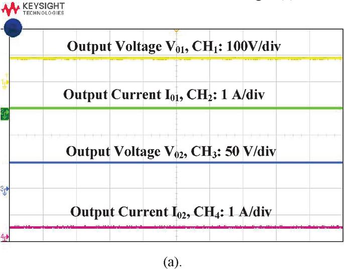
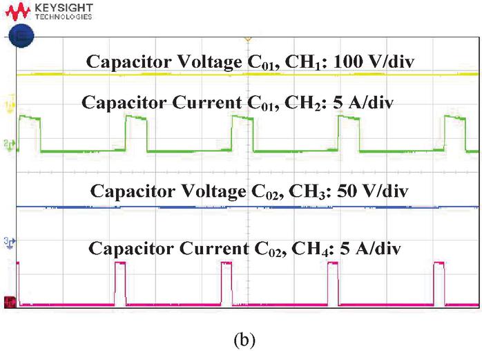
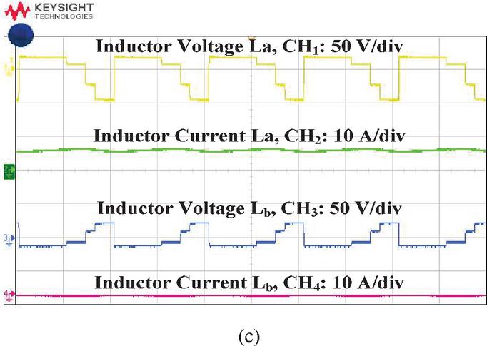
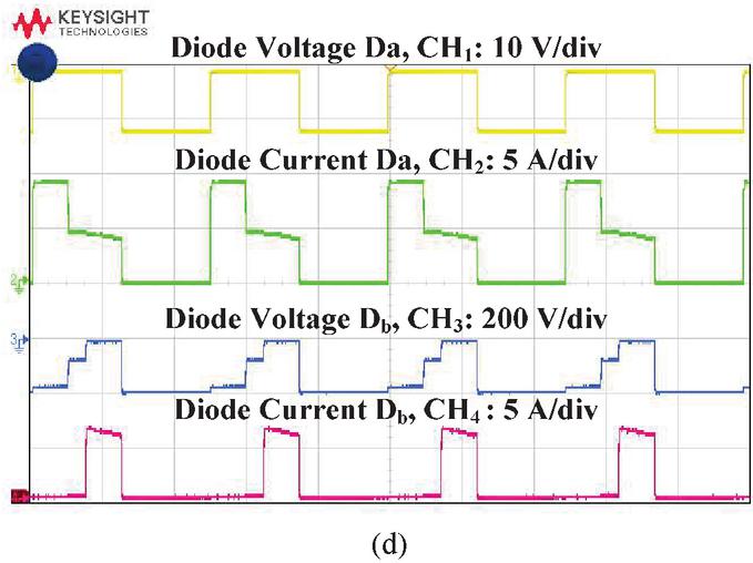
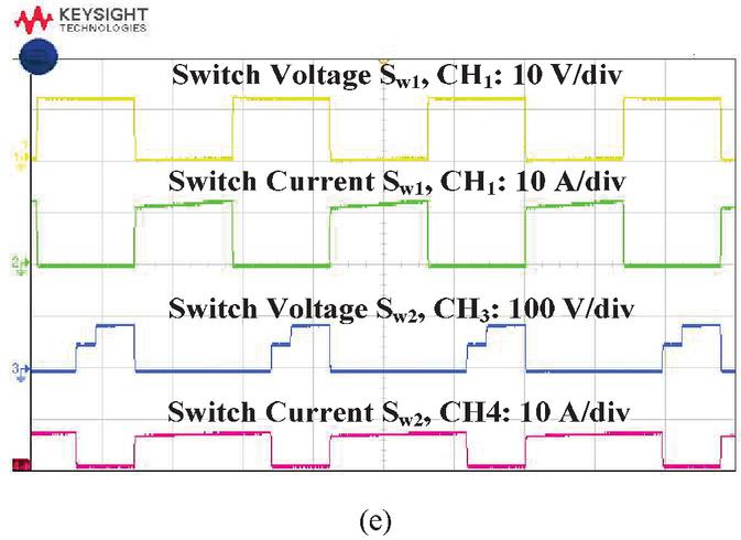
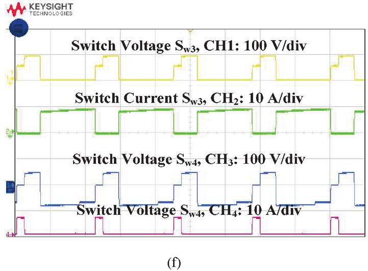
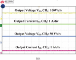
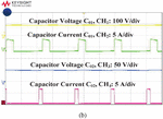
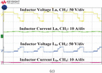
To assess the working of projected converter in real time conditions, hardware prototype has been developed and experimental waveforms are analysed. The output voltage waveforms are displayed in Figure 6(a). The switching frequency of 20 KHz is opted for the pulse generation. The experimental waveform analysis is exactly matching with the results attained from the simulation. The hardware waveforms of inductors, capacitors, diodes and switches are also strictly adhere with the simulation results and are shown in Figure 6(b–f). From Figure 6(a) it is clearly noticed that the load voltage across the loads R and R are 118 V and 60 V respectively and that satisfies the converter performance in a realistic condition. Similarly, the charging and discharging status of both the inductors are exactly matched with the simulation waveforms as shown in Figure 6(c).
Figure 6 (a–f). Experimental waveforms of various voltages and currents.
The relative analysis of introduced converter is done in terms of component counts (passive and active components), the count of input sources and output ports with other projected converter topologies in the literature and the results are represented in Table 2. The study of comparison discloses that the presented converter has lower count of the components when compared with other topologies, so that overall circuit complexity and losses can be reduced to a great extent.
Table 2 Comparison table with other converters
| Component Comparison | |||||||
| S. No | Parameters | Presented Converter | [2] | [10] | [13] | [14] | [17] |
| 1. | Switch counts | 4 | 3 | 2 | 4 | 4 | 6 |
| 2. | Diode counts | 2 | 5 | 2 | 4 | 5 | 3 |
| 3. | Inductors counts | 2 | 2 | 6 | 1 | 2 | 2 |
| 4. | Capacitors counts | 2 | 1 | 4 | 2 | 2 | 5 |
| 5. | Total Elements | 10 | 12 | 15 | 13 | 16 | 17 |
| 6. | Output voltage levels | 2 | 1 | 1 | 2 | 1 | 1 |
| 7. | Input Sources | 2 | 2 | 2 | 2 | 3 | 2 |
5 Conclusion
In this paper, a dual inductor based two input two output boost type DC-DC converter is introduced to achieve higher voltage gain with lower component counts and better performance that can be incorporated for electric vehicle/DC microgrid applications. The power switches in the given converter are well suited to operate with flexible duty ratios which is one of the significant advantages of the converter. Thorough analysis of the converter in steady state condition is presented with the help of supporting circuits and equations. Then the converter performance is evaluated under simulation and experimental backgrounds and the waveforms are described. Finally, the converter is compared with other well-known topologies based on the number of ports, passive and active component counts etc., and from the analysis it is found that the introduced converter has reasonably lower part count that reduces the overall circuit intricacy and enhances the converter role in the applications of dc microgrid, EV etc.
References
[1] X. Wu, W. Shi and J. Du, “Dual-Switch Boost DC–DC Converter for Use in Fuel-Cell-Powered Vehicles,” in IEEE Access, vol. 7, pp. 74081–74088, 2019, DOI: 10.1109/ACCESS.2019.2917529, May 2019.
[2] S. Athikkal, “Performance Evaluation of A Positive Output Voltage Dual Input DC–DC Converter,” 2021 2nd International Conference for Emerging Technology (INCET), Belagavi, India, 2021, pp. 1–5, doi: 10.1109/INCET51464.2021.9456377.
[3] Z. Shan, X. Ding, J. Jatskevich and C. K. Tse, “Synthesis of Multi-Input Multi-Output DC/DC Converters Without Energy Buffer Stages,” in IEEE Transactions on Circuits and Systems II: Express Briefs, vol. 68, no. 2, pp. 712–716, DOI: 10.1109/TCSII.2020.3015388, Feb-2021.
[4] G. Chen, Y. Liu, X. Qing, M. Ma and Z. Lin, “Principle and Topology Derivation of Single-Inductor Multi-Input Multi-Output DC–DC Converters,” in IEEE Transactions on Industrial Electronics, vol. 68, no. 1, pp. 25–36, DOI: 10.1109/TIE.2020.2965490, Jan 2021.
[5] H. Behjati and A. Davoudi, “Single-stage multi-port DC-DC converter topology,” IET Power Electron., vol. 6, no. 2, pp. 392–403, DOI: 10.1049/iet-pel.2012.0339, Feb. 2013.
[6] P. Mohseni, S. H. Hosseini, M. Sabahi, T. Jalilzadeh and M. Maalandish, “A New High Step-Up Multi-Input Multi-Output DC–DC Converter,” in IEEE Transactions on Industrial Electronics, vol. 66, no. 7, pp. 5197–5208, DOI: 10.1109/TIE.2018.2868281, July 2019.
[7] G. Chen, Z. Jin, Y. Deng, X. He and X. Qing, “Principle and Topology Synthesis of Integrated Single-Input Dual-Output and Dual-Input Single-Output DC–DC Converters,” in IEEE Transactions on Industrial Electronics, vol. 65, no. 5, pp. 3815–3825, DOI: 10.1109/TIE.2017.2760856, May 2018.
[8] H. Kim, J. Maeng, I. Park, J. Jeon, D. Lim and C. Kim, “A 90.2% Peak Efficiency Multi-Input Single-Inductor Multi-Output Energy Harvesting Interface with Double-Conversion Rejection Technique and Buck-Based Dual-Conversion Mode,” in IEEE Journal of Solid-State Circuits, vol. 56, no. 3, pp. 961–971, DOI: 10.1109/JSSC.2020.3025722, March 2021.
[9] S. Athikkal, C. Bharatiraja, B. Lehman and T. B. Lazzarin, “Performance Evaluation of A Dual Input Hybrid Step up DC-DC Converter,” 2020 International Conference on Power, Instrumentation, Control and Computing (PICC), pp. 1–6, DOI: 10.1109/PICC51425.2020.9362473, Dec. 2020.
[10] Z. Saadatizadeh, P. C. Heris, X. Liang and E. Babaei, “Expandable Non-Isolated Multi-Input Single-Output DC-DC Converter with High Voltage Gain and Zero-Ripple Input Currents,” in IEEE Access, vol. 9, pp. 169193–169219, 2021, DOI: 10.1109/ACCESS.2021.3137126, Dec. 2021.
[11] M. Forouzesh, Y. P. Siwakoti, S. A. Gorji, F. Blaabjerg and B. Lehman, “Step-Up DC–DC Converters: A Comprehensive Review of Voltage- Boosting Techniques, Topologies, and Applications,” in IEEE Transactions on Power Electronics, vol. 32, no. 12, pp. 9143–9178, DOI: 10.1109/TPEL.2017.2652318, Dec. 2017.
[12] S. Athikkal and K. M. R. Eswar, “A Three Input Dual Output Boost Type Non-Isolated DC-DC Converter,” 2021 International Conference on Intelligent Technologies (CONIT), 2021, pp. 1–6, DOI: 10.1109/CONIT51480.2021.9498433, Jun. 2021.
[13] X. L. Li, Z. Dong, C. K. Tse and D. D. -C. Lu, “Single-Inductor Multi-Input Multi-Output DC–DC Converter with High Flexibility and Simple Control,” in IEEE Transactions on Power Electronics, vol. 35, no. 12, pp. 13104–13114, DOI: 10.1109/TPEL.2020.2991353, Dec. 2020.
[14] R. R. Ahrabi, H. Ardi, M. Elmi and A. Ajami, “A Novel Step-Up Multiinput DC–DC Converter for Hybrid Electric Vehicles Application,” in IEEE Transactions on Power Electronics, vol. 32, no. 5, pp. 3549–3561, DOI: 10.1109/TPEL.2016.2585044, May 2017.
[15] K. Suresh et al., “A Multifunctional Non-Isolated Dual Input-Dual Output Converter for Electric Vehicle Applications,” in IEEE Access, vol. 9, pp. 64445–64460, 2021, doi: 10.1109/ACCESS.2021.3074581
[16] Jyotheeswara Reddy K, Sudhakar Natarajan, “Energy Sources and Multi-Input DC-DC Converters used in Hybrid Electric Vehicle Applications – A Review,” International Journal of Hydrogen Energy, vol. 43, pp. 17378–17408, DOI: 10.1016/j.ijhydene.2018.07.076, Sep. 2018.
[17] R. Faraji, L. Ding, T. Rahimi, H. Farzanehfard, H. Hafezi and M. Maghsoudi, “Efficient Multi-Port Bidirectional Converter with Soft-Switching Capability for Electric Vehicle Applications,” in IEEE Access, vol. 9, pp. 107079–107094, 2021, DOI: 10.1109/ACCESS.2021.3097750, Jul. 2021.
[18] A. Hintz, U. R. Prasanna and K. Rajashekara, “Novel Modular Multiple-Input Bidirectional DC–DC Power Converter (MIPC) for HEV/FCV Application,” in IEEE Transactions on Industrial Electronics, vol. 62, no. 5, pp. 3163–3172, DOI: 10.1109/TIE.2014.2371778, May 2015.
[19] K. M. Nisar, A. Sivaprasad, S. Kumaravel and P. Ananthakrishnan, “Implementation of closed loop controller in a dual input DC-DC converter for DC-microgrid application,” 2016 IEEE Annual India Conference (INDICON), pp. 1–6, DOI: 10.1109/INDICON.2016.7839111, Dec. 2016.
[20] Sivaprasad Athikkal, Kumaravel Sundaramoorthy, Ashok Sankar, “A Modified Dual Input DC-DC Converter for Hybrid Energy Application,” International Journal of Power Electronics and Drive System (IJPEDS)., vol. 8, no. 1, pp. 81–92, DOI: 10.11591/ijpeds.v8.i1, Mar. 2017.
Biographies

R. Aravind was born in Chengalpattu, India, in 1988. He received the diploma Degree from Adhiparasakthi Polytechnic College, Melmaruvathur, India, in 2007, B.E. Degree from P.M.R. Institute of Technology, India, in 2010, and the M.Tech. Degree from SRM University, Kattankulathur, India, in 2014. He is currently Pursuing towards his Ph.D. Degree in the Department of Electrical and Electronics Engineering, SRM Institute of Science and Technology – Main campus, Kattankulathur, Chennai, India. His research interest includes Multi-port DC-DC converters, high gain DC-DC converters and their application in Electric Vehicle, DC Microgrid etc.

Sivaprasad Athikkal was born in Thrissur, India, in 1989. He received the B.Tech. degree in Electrical and Electronics Engineering from University of Calicut, Thenhippalam, India, in 2010, and the M.Tech. degree in Power Electronics from the Amrita Vishwa Vidyapeetham University, Coimbatore, India, in 2012, and Ph.D. degree in Electrical Engineering from National Institute of Technology Calicut, India in 2018. He is currently working as an Assistant Professor with the department of Electrical and Electronics Engineering, Muthoot Institute of Technology and Science, Ernakulam, India. He received young researcher award by Institute of Scholars India in 2020. He is the recipient of best paper awards in ICATCHCOME 2022 and EPREC 2022 international conferences organized by KPRIET and NIT Jamshedpur respectively. His main research interests include multiple input DC–DC converters, high gain DC-DC converters, renewable energy integration, and distributed generation.

Ravi Eswar Kodumur Meesala was born in Kurnool, India, in 1993. He received the B.Tech. Degree from Jawaharlal Nehru Technological University, Ananthapur, India, in 2014, and the M.Tech. Degree from Vellore Institute of Technology, Vellore, India, in 2016. He achieved third rank in M. Tech (Power Electronics and Drives), Vellore Institute of Technology, Vellore. He received the Ph.D. degree from National Institute of Technology, Warangal, India, in 2020. He is currently an Assistant professor with the Department of Electrical and Electronics Engineering, SRM Institute of Science and Technology – Main campus, (Category I University, NAAC: A Grade, Engineering NIRF – 41 rank), Kattankulathur-603203, Chennai, India. He received gold medal for his research excellence presentation on “Modified Direct Torque Control of PMSM Drive for Electric Vehicle Application” held at SRM Institute of Science and Technology-Kattankulathur, India. He has authored several scientific papers in the field of electric motor drives, published in reputed journals of Electrical and Electronics Engineering (IEEE Transactions and Journals, IET Journals, and T & F Journals). He acted as a resource person to deliver talk on Electric Vehicles in Faculty Development Programs sponsored by AICTE and ISTE. His current research interests include electric motor drives, power electronics and power converter circuits.

K. Jyotheeswara Reddy has more than 7 years of teaching experience in various reputed institutions/universities. He has actively participated in all the academic and administrative activities at various levels and produced succeeded results in academia and research. He completed his Bachelor degree from JNTU-Kakinada and Master’s degree from Sathyabama University, Chennai. He completed his Ph. D degree from VIT University. He served as an Associate Professor in Sree Vidyanikethan Engineering College, Tirupathi. Presently, he is working as an Associate Professor in School of Electrical and Electronics Engineering, REVA University-Bangalore. He has authored and coauthored more than 15 publications in reputed International Journals (SCI & Scopus Indexed Journals) and conferences.
He is a member of IEEE and IAENG. He served as Conference organizer, Session Chair, Technical Program Committee, reviewer of many reputed journals including IEEE/Elsevier/Springer etc. His research area includes Power Electronic Converters, Renewable Energy Sources and Electric Vehicles.

Ritesh Dash, received his Ph. D from School of Electrical Engineering, KIIT University and presently working as Associate Professor at REVA University, Bangalore. He has a research experience of over 10 years and has sound knowledge in the field of Artificial Intelligence, FACTS and Machine learning. He has published more than 100 numbers of research papers both in International Journal and Conference. Earlier he has also published a book under CRC press. He has also served the Govt. of India as a Design Engineer, Electrical at WAPCOS Ltd. A Central PSU under Ministry of Water Resources & Ganga Rejuvenation. His current research interests include Artificial Intelligence and Machine learning in high voltage engineering applications.
He has received Madhusudan Memorial Award and Institutional Award from the Institution of Engineers, India. He is associated with Many International Bodies such as IEEE, Indian Science Congress, The Institution of Engineers, Solar Energy Society of India, Carbon Society of India and Many More.

Vivekanandan Subburaj received the B.E. and M.E. degrees in electrical and electronics engineering from Anna University, Chennai, India, in 2011 and 2013, respectively, and the Ph.D. degree from the Electrical and Electronics Engineering Department, National Institute of Technology Karnataka (NITK), Mangalore, India, in 2019. He awarded University Rank Holder in his M.E degree. He was with NITK, where he was involved in low power circuit design. Further, He served as an Associate Professor in REVA University, Bengaluru, India. He joined the Electrical Engineering department, NIT Silchar, India, in 2022, where he is currently an Assistant Professor. His current research interests include low-voltage dc–dc converter topology design with particular emphasis on low power electronics for portable computing and power management IC and power chargers.
V. Subburaj was the recipient of the Best Paper Award in Asia Flagship Conference TENCON 18. He is the Member of IEEE. He served as Editorial board member of many conference committees. Published his research articles in high impact journals such as, IEEE Transaction, IET, Elsevier etc., He served as guest editor for SCOPUS and Web of Science Journals. He organized Scopus index conferences, IEEE conferences and supported many workshops and training programs conducted by the government organization.
Distributed Generation & Alternative Energy Journal, Vol. 38_3, 943–964.
doi: 10.13052/dgaej2156-3306.38310
© 2023 River Publishers
