A Two-Input Single-Output Boost Converter with Fault Tolerant Operation
K. Karishma1, A. Sivaprasad2 and Nithin Raj1
1Department of Electrical Engineering, Rajiv Gandhi Institute of Technology, Kottayam, Kerala, India
2Department of Electrical & Electronics Engineering, Muthoot Institute of Technology and Science, Kochi, Kerala, India
E-mail: nithinrmu@gmail.com
*Corresponding Author
Received 28 June 2023; Accepted 29 January 2024
Abstract
The need for multi-input DC-DC converters is highly demanded in the context of the integration of different energy sources. When integrating several energy sources, such as batteries, solar PV arrays, fuel cells, etc., multi-input DC-DC converters preferred over multiple single-input DC-DC converters. The vast majority of MISO converters in use today only have one mode of operation, which is conventional operation using all sources. Very few MISO topologies have been presented with fault-tolerant capability. In this work, a non-isolated two-input single-output (MISO) boost converter is investigated for low-voltage DC (LVDC) applications with fault tolerant capability. The presented converter works in three modes, such as DC sources of equal values, DC sources of unequal values, and one of the DC sources that is faulty or out of order. The converter is simulated in a MATLAB/Simulink environment and experimentally validated using a scaled prototype. The outcomes demonstrate that the converter can integrate systems with two DC energy sources, accommodates DC sources of equal values, DC sources of unequal values, and works even when one of the DC sources is faulty or out of order. This work points out that the presented MISO converter would be an apt solution for integrating varying input voltage sources with fault-tolerant capability.
Keywords: Non-isolated boost converter, multi-input single-output converter, low voltage DC application, renewable energy sources, fault tolerant operation.
1 Introduction
The use of batteries, solar PV arrays, fuel cells, etc. has expanded as a result of the increased focus on renewable energy sources for sustainable development [1–3]. Such a distributed system needs the integration of power from various sources into a common grid. Traditionally, integrated DC-DC converters are used to integrate power from several energy sources. Multi-input single-output (MISO) DC-DC converters have been established in order to optimize operation in a high-performance and cost-effective manner. The main advantage of the MISO converter is the reduced component count and increased power handling capacity [4, 5]. Recently, MISO converters have been an active area of research for renewable energy integration and electric vehicle applications [6–8].
Over the decade, a number of multi-input converter topologies have been presented, a comprehensive review of such topologies is presented in [9]. A two-input single output topology is proposed in [10], the main drawback is the negative polarity. A bridge-type MISO converter topology with improved performance is presented in [11, 12]. A simple topology for a two-input single-output converter is presented in [13], and an extended version is presented in [14]. Furthermore, a T-type non-isolated two-input topology is investigated in [15]. There are different topologies presented with buck, boost, buck-boost operating modes integrated into the same topology [16, 17]. A SEPIC converter-based two-input single-out converter is examined in [18]. These topologies each have their own benefits and drawbacks in terms of component count, voltage gain, etc. It should be emphasized that the vast majority of MISO converters in use today operate in just one mode, i.e., the typical operating mode, with all sources available. In the present scenario, reliable and continuous operation of the entire system is demanded.
Though many of the MISO converters have advantages of voltage gain and control simplicity, the number of component counts used raises the likelihood of faults in the system. This has redirected the focus to fault tolerant operation of multi-input converters in addition to development of topologies with reduced count or voltage gain [19]. A study on the MISO converter with fault-tolerant operation is urgently needed in this situation, which is the primary driving force for this work. A two-input ingle output boost converter topology is presented in [20]. This topology integrates two inputs sources and accommodates source voltage variation and one source fault condition. This peculiar DC-DC converter is investigated in this work, to validate the operating modes and the fault tolerant capacity of the converter. The circuit topology and its operating modes are described in Section 2. The results of the simulation study are explained in Section 3. In Section 4, the hardware setup and experimental validation are described. Section 5 then offers a conclusion.
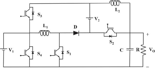
Figure 1 Two-input single output boost converter circuit topology.
2 Circuit Topology and Modes of Operation
The two-input single-output boost converter topology is depicted in Figure 1 [20]. The circuit consist of two DC sources (V, V), four switches (S, S, S, S), one diode (D), two inductors (L, L), one filter capacitor (C) and load resistance (R). The DC sources can be batteries, Solar PV, fuel cell, etc. This circuit can work in three different modes, as follows.
2.1 Mode-1: Both Sources are Available with Same Voltages
In this mode, both sources are available with same voltages (V V). Here, two cases are there, Case-1: inductors are being energized and Case-2: inductors are being discharged. The output voltage equation in this mode is given as follows.
| (1) |
where, V V V and D is the duty ratio.
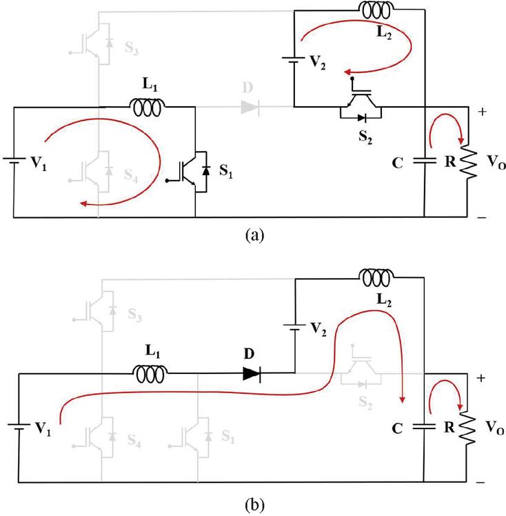
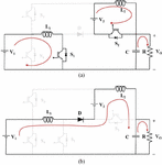
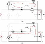
Case-1: In this case, switches (S, S) are provided with gate pulses and S, D and D remains in off conditions, as illustrated in Figure 2(a). The inductors (L, L) energize from sources (V, V) and the capacitor (C) discharges though the load. Case-2: In this case, all the switches remain in off conditions, as illustrated in Figure 2(b). The inductors (L, L) deenergize to capacitor (C) and load resistance (R) thought the diode (D).
Figure 2 Mode-1 equivalent circuits: (a) inductors being energized (b) inductors being deenergized.
2.2 Mode-2: Both Sources are Available with Different Voltages
In this mode, both sources are available with same voltages (V V). Here also, two cases are there, Case-1: inductors are being energized and Case-2: inductors are being discharged. These two cases will be same as that of the Mode-1 and the equivalent circuits are same as shown in Figure 2. The output voltage equation in this mode is given as follows.
| (2) |
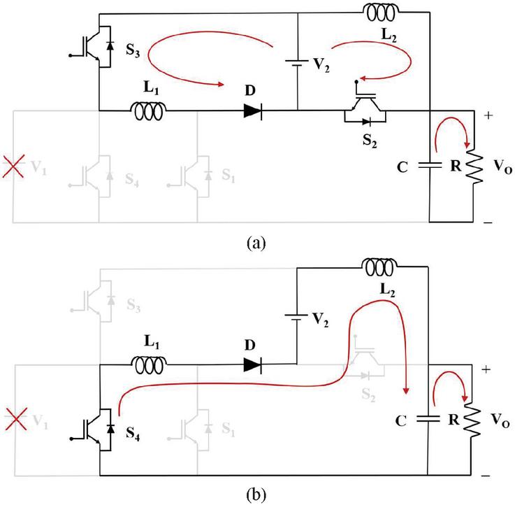
Figure 3 Mode-3 equivalent circuits: (a) inductors being energized (b) inductors being deenergized.
2.3 Mode-3: One of the Input Sources is Out of Work
In this mode, Source-1 (V) is faulty/out of order. In such a case, the inductors (L, L) are energized from the Source-2 (V). Here also, two cases are there, Case-1: inductors are being energized and Case-2: inductors are being discharged. The output voltage equation in this mode is given as follows.
| (3) |
Case-1: In this case, the inductors (L, L) are energized from the Source-2 (V) through the switches S, S, and D. as illustrated in Figure 3(a). Case-2: The inductors (L, L) deenergize to capacitor (C) and load resistance (R) though the switch (S) diode (D), as illustrated in Figure 3(b).
3 Simulation Study
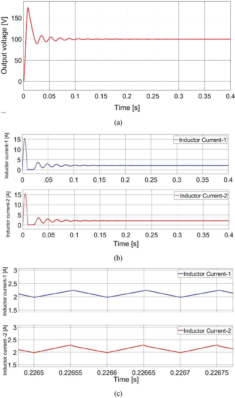
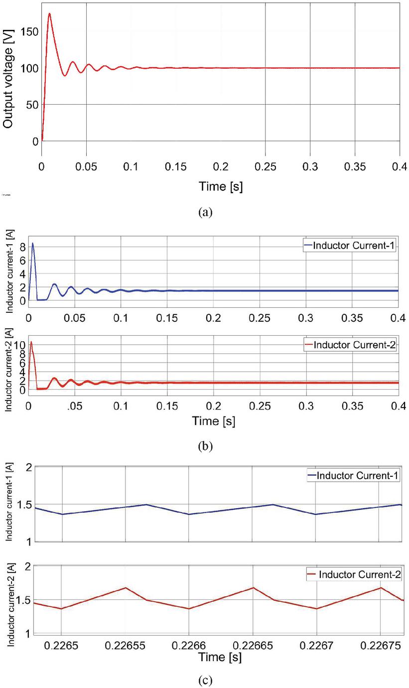
The circuit shown in Figure 1 is simulated in MATLAB/Simulink environment for the three modes described in the previous section. The simulation parameters are given in Table 1. Mode-1: the circuit diagram shown in Figure 1 is simulated in MATLAB/Simulink with the following parameters V V 25V and duty ratio of 50%. The simulated waveform of output voltage, inductor currents and a zoomed version of inductor currents are shown in Figure 4(a)–(c).
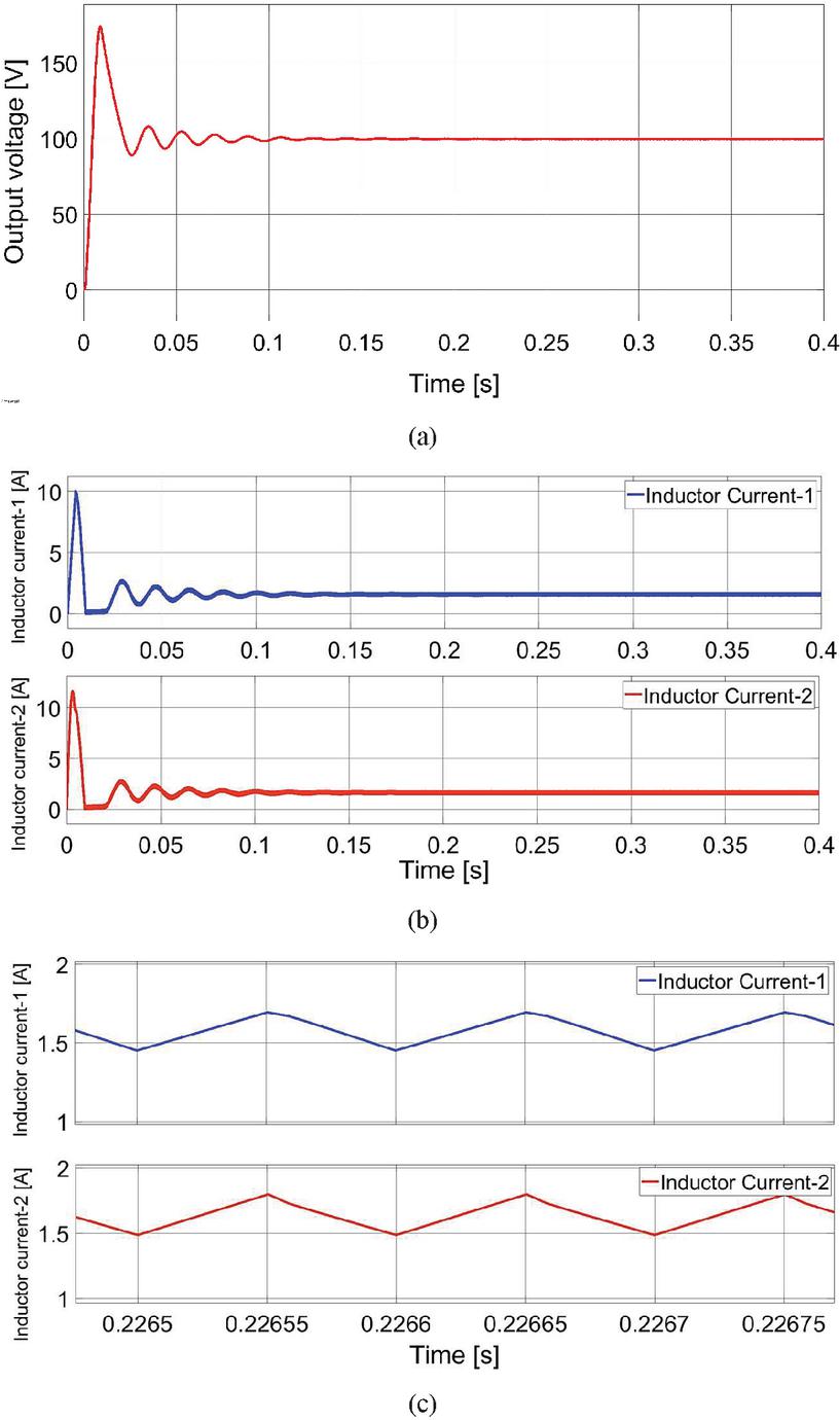
Mode-2: the circuit diagram shown in Figure 1 is simulated in MATLAB/Simulink with the following parameters V 10V, V 25V. The simulated waveform of output voltage, inductor currents and a zoomed in version of inductor currents are shown in Figure 5(a)–(c). Mode-3: the circuit diagram shown in Figure 1 is simulated in MATLAB/Simulink with the following parameters V 0V, V 25V. The simulated waveform of output voltage, inductor currents and a zoomed in version of inductor currents are shown in Figure 6(a)–(c).
| Parameter | Value |
| Input Voltages (V, V) | 25V |
| Output Voltage | 100V |
| Input Current (Peak) | 2A |
| Switching Frequency | 10kHz |
| Inductors (L, L) | 5mH, 4mH |
| Capacitors | 180 F |
Figure 4 Simulation results of mode-1 (a) output voltage (b) inductor currents (c) zoomed view of inductor currents.
Figure 5 Simulation results of mode-2 (a) output voltage (b) inductor currents (c) zoomed view of inductor currents.
Figure 6 Simulation results of mode-3 (a) output voltage (b) inductor currents (c) zoomed view of inductor currents.
4 Experimental Validation and Discussion
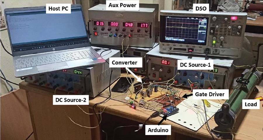
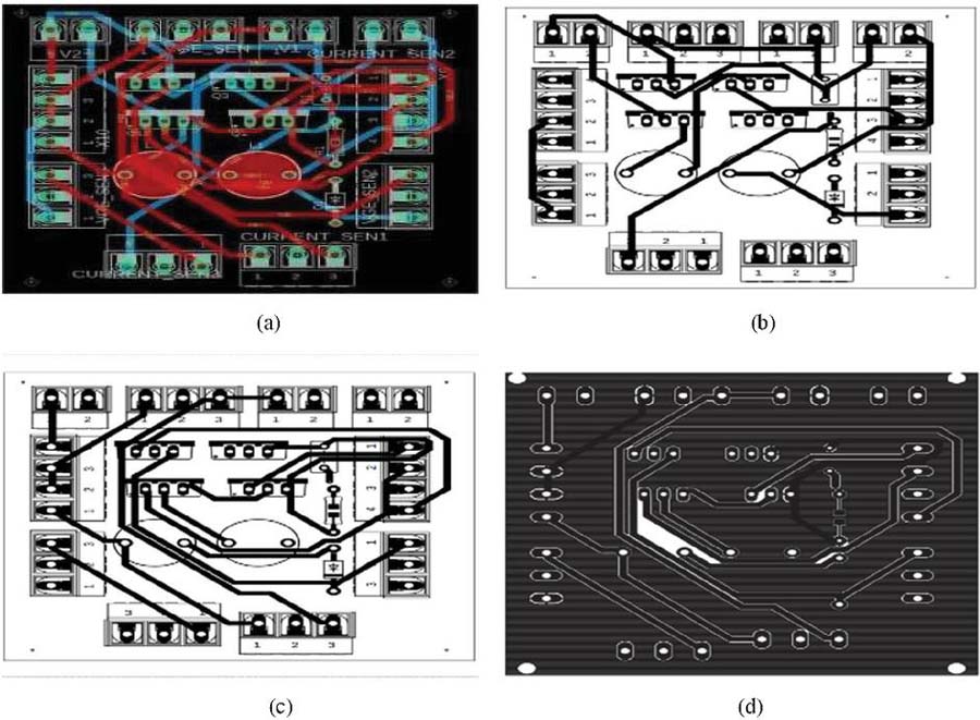
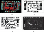
An experimental prototype shown in Figure 7 is used to validate the converter operation. The specifications are shown in Table 2. IRF540 MOSFETs with TLP250 driver IC are used. ACS sensors are used for current measurement. The program to generate gate pulses for the converter is implemented on Arduino control board. Different stages of the PCB development are shown in Figure 8.
Table 2 Hardware specifications
| Parameter | Value |
| Input Voltages (V, V) (Max) | 12V |
| Output Voltage (Max) | 60V |
| Input Current (Peak) | 2A |
| Switching Frequency | 10kHz |
| Inductors (L, L) | 5mH, 4mH |
| Capacitors | 220 F |
Figure 7 Overall experimental setup.
Figure 8 PCB development (a) PCB footprint (b) bottom layer (c) top layer (d) masked layer.
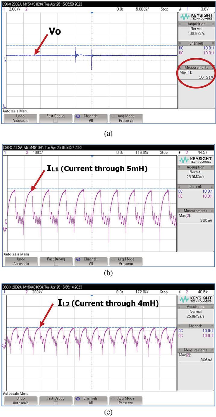
The measured value of the output voltage and inductor currents with the following parameters V V 4V and duty ratio of 60% are shown in Figure 9(a)–(c). An output voltage of 16.21V and the inductor currents are proportionate to the inductor values (5mH and 4mH) obtained. It can be confirmed that the experimental results closely match with the simulation results and the theoretical values obtained.
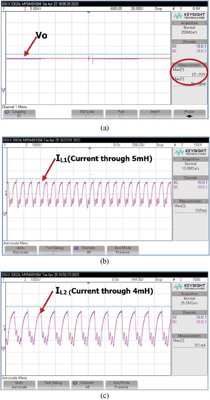
The measured value of the output voltage and inductor currents with the following parameters V 3V, V 4V and duty ratio of 45% are shown in Figure 10(a)–(c). An output voltage of 15.02V and the inductor currents are proportionate to the inductor values (5mH and 4mH) obtained. It can be confirmed that the experimental results closely match with the simulation results and the theoretical values obtained from Equation (2).
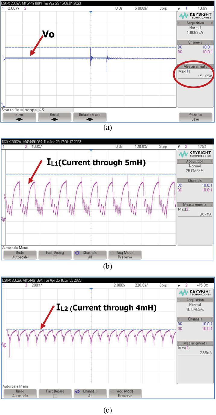
The measured value of the output voltage and inductor currents with the following parameters V 0V, V 4V and duty ratio of 60% are shown in Figure 11(a)–(c). An output voltage of 15.65V and the inductor currents are proportionate to the inductor values (5mH and 4mH) obtained. It can be confirmed that the experimental results closely match with the simulation results and the theoretical values obtained from Equation (3).
Figure 9 Measured waveforms of mode-1 (a) output voltage (b) inductor current-1 (c) inductor current-2.
Figure 10 Measured waveforms of mode-2 (a) output voltage (b) inductor current-1 (c) inductor current-2.
Figure 11 Measured waveforms of mode-3 (a) output voltage (b) inductor current-1 (c) inductor current-2.
In this research work, a MISO converter is investigated and experimentally validated. The results confirm that the presented converter boosts the input voltage to the necessary output level regardless of the input voltage values, including both the same values and different values (modes 1 and 2). The mode-3 results show that the presented converter can cope with the failure or unavailability of one source (source-1), allowing for the system’s reliable and continuous functioning. Based on this work, the adaptability of the presented MISO converter with changing input voltage source and fault tolerant operation is proven. This point out that this converter is a viable option for integration of variable input sources. Additionally, the flexibility to use a single source means that the converter is ideally suited for the integration of PV solar sources, where lack of continuous is a common problem. The converter that has been investigated is therefore a feasible way to integrate a variety of inputs from batteries, solar PV, fuel cells, etc. in applications like LVDC systems, renewable energy integration, electric vehicles, etc.
5 Conclusions
A two-input, single-output, non-isolated boost converter is demonstrated in this study. For the integration of several DC sources, the architecture does not call for the need of two separate DC-DC converters. Additionally, this converter functions well with sources of fluctuating DC input. Additionally, the converter continues to function even if one of the DC sources is unavailable, ensuring the total system’s dependable and continuous operation. Through simulation and experimentation, the converter’s validity and efficacy are confirmed. Furthermore, to manage the initial overshoot and steady-state accuracy, a controller/compensator can be built and a closed-loop control must be implemented. Therefore, the converter that has been presented is a suitable method for integrating numerous DC inputs from batteries, solar PV, fuel cells, etc. in applications like electric vehicles, LVDC systems, integrating renewable energy, standalone solar PV systems, etc.
References
[1] Harinaik, S. and Sathyan, S., “Design and Analysis of Quasi-Y Source High Gain DC/DC Resonant Converter for Renewable Energy Applications”, in Distributed Generation & Alternative Energy Journal, vol. 38, no. 02, 569–594, 2023. DOI: 10.13052/dgaej2156-3306.3829.
[2] Saahithi, S., Kumar, B. H., Reddy, K. J., Dash, R., and Subburaj, V., “Four Speed Auto Transmission DC-DC Converter Control for E-Vehicle and Regenerative Braking Based on Simulation and Model Investigation”, in Distributed Generation & Alternative Energy Journal, vol. 38, no. 03, 987–1006, 2023. DOI: 10.13052/dgaej2156-3306.38312.
[3] Reddy, B. R. S, Reddy, V. C. V, and Kumar, M. V., “Design and Analysis of DC-DC Converters with Artificial Intelligence Based MPPT Approaches for Grid Tied Hybrid PV-PEMFC System”, in Distributed Generation & Alternative Energy Journal, vol. 38, no. 04, 1307–1330, 2023. DOI: 10.13052/dgaej2156-3306.38410.
[4] X. L. Li, Z. Dong, C. K. Tse and D. D.-C. Lu, “Single-Inductor Multi-Input Multi-Output DC–DC Converter With High Flexibility and Simple Control,” in IEEE Transactions on Power Electronics, vol. 35, no. 12, pp. 13104–13114, Dec. 2020, DOI: 10.1109/TPEL.2020.2991353.
[5] Z. Shan, X. Ding, J. Jatskevich and C. K. Tse, “Synthesis of Multi-Input Multi-Output DC/DC Converters Without Energy Buffer Stages,” in IEEE Transactions on Circuits and Systems II: Express Briefs, vol. 68, no. 2, pp. 712–716, Feb. 2021, DOI: 10.1109/TCSII.2020.3015388.
[6] Aravind, R., Athikkal, S., Meesala, R. E. K., Reddy, K. J., Dash, R., and Subburaj, V. (2023). Dual Inductor Based Two Input Two Output DC-DC Converter and its Analysis for DC Microgrid Application. Distributed Generation & Alternative Energy Journal, 38(03), 943–964. https:/doi.org/10.13052/dgaej2156-3306.38310.
[7] S. R. Khasim, C. Dhanamjayulu and S. M. Muyeen, “A Single Inductor Multi-Port Power Converter for Electric Vehicle Applications,” in IEEE Access, vol. 11, pp. 3367–3385, 2023, DOI: 10.1109/ACCESS.2023.3234105.
[8] P. Gunawardena, N. Hou, D. Nayanasiri and Y. Li, “A Dual-Input Single-Output DC-DC Converter Topology for Renewable Energy Applications,” in IEEE Transactions on Industry Applications, vol. 59, no. 2, pp. 1995–2006, March–April 2023, DOI: 10.1109/TIA.2022.3218619.
[9] A. H. Chander, L. K. Sahu and P. T. Bankupalli, “Review on General Architecture and Selection of Multiple Input Converters,” 2020 First International Conference on Power, Control and Computing Technologies (ICPC2T), Raipur, India, 2020, pp. 240–245, DOI: 10.1109/ICPC2T48082.2020.9071457.
[10] Kushal K., Madhuri C., “Experimental realization of a multi-input buckboost DC-DC converter,” Turkish Journal of Electrical Engineering & Computer Sciences, vol. 26, no. 3, pp. 1453–1469, 2018. https:/doi.org/10.3906/elk-1703-366.
[11] Athikkal, S.; Sundaramoorthy, K.; Sankar, A. Design, Fabrication and Performance Analysis of a Two Input-Single Output DC-DC Converter. Energies, vol. 10, no. 9, pp. 2–18, 2017, https:/doi.org/10.3390/en10091410.
[12] Sivaprasad A., G. G. Kumar, Kumaravel S. and Ashok S., “A novel bridge type DC-DC converter for hybrid energy source integration,” 2016 IEEE 1st International Conference on Power Electronics, Intelligent Control and Energy Systems (ICPEICES), Delhi, India, 2016, pp. 1–6, DOI: 10.1109/ICPEICES.2016.7853302.
[13] A. Sivaprasad, J. Joseph, S. Kumaravel and S. Ashok, “Design and analysis of a dual input DC-DC converter for hybrid electric vehicle,” 2015 IEEE International Conference on Signal Processing, Informatics, Communication and Energy Systems (SPICES), Kozhikode, India, 2015, pp. 1–5, DOI: 10.1109/SPICES.2015.7091466.
[14] S. Athikkal, C. Bharatiraja, B. Lehman and T. B. Lazzarin, “Performance Evaluation of A Dual Input Hybrid Step up DC-DC Converter,” 2020 International Conference on Power, Instrumentation, Control and Computing (PICC), Thrissur, India, 2020, pp. 1–6, DOI: 10.1109/PICC51425.2020.9362473.
[15] S. Athikkal, R. E. Kodumur Meesala, J. Peter, R. Kumar, R. K. Singh and A. Kumar, “A Two Input Two Output Step Up Type Transformerless DC-DC Converter,” 2021 Fourth International Conference on Electrical, Computer and Communication Technologies (ICECCT), Erode, India, 2021, pp. 1–6, DOI: 10.1109/ICECCT52121.2021.9616892.
[16] A. Sivaprasad, J. Joseph, S. Kumaravel and S. Ashok, “Design and analysis of a dual input DC-DC converter for hybrid electric vehicle,” 2015 IEEE International Conference on Signal Processing, Informatics, Communication and Energy Systems (SPICES), Kozhikode, India, 2015, pp. 1–5, DOI: 10.1109/SPICES.2015.7091466.
[17] A. Elshora and H. A. Gabbar, “Design and Analysis of Multi-Input, Single-Output, Nonisolated DC/DC Converter for Fast Charging of Electric Vehicles,” 2021 International Conference on Electrical, Computer, Communications and Mechatronics Engineering (ICECCME), Mauritius, Mauritius, 2021, pp. 1–7, DOI: 10.1109/ICECCME52200. 2021.9591071.
[18] S. A. Yasin, J. Kumar, Y. Kumar, S. Athikkal and J. Peter, “Analysis of a Dual Input DC-DC Converter Topology Based on SEPIC Configuration,” 2019 International Conference on Power Electronics Applications and Technology in Present Energy Scenario (PETPES), Mangalore, India, 2019, pp. 1–6, DOI: 10.1109/PETPES47060.2019.9003780.
[19] A. H. Chander, L. K. Sahu and M. Jalhotra, “Reliability analysis of Multiple Input Converter,” 2020 First International Conference on Power, Control and Computing Technologies (ICPC2T), Raipur, India, 2020, pp. 235–239, DOI: 10.1109/ICPC2T48082.2020.9071517.
[20] M. Dhananjaya and S. Pattnaik, “Design and Implementation of a Multi-Input Single-Output DC-DC Converter,” 2019 IEEE International Conference on Sustainable Energy Technologies and Systems (ICSETS), Bhubaneswar, India, 2019, pp. 194–199, DOI: 10.1109/ ICSETS.2019.8744815.
Biographies

K. Karishma completed bachelor’s degree at Sree Narayana Institute of Technology in Adoor in Electrical and Electronics Engineering. Currently, she is pursuing a master’s degree in power systems and renewable energy at the in the Department of Electrical Engineering, Rajiv Gandhi Institute of Technology in Kottayam.

A. Sivaprasad was born in Thrissur, India, in 1989. He received the B.Tech. degree in Electrical and Electronics Engineering from University of Calicut, Thenhippalam, India, in 2010, and the M. Tech. degree in Power Electronics from the Amrita Vishwa Vidyapeetham University, Coimbatore, India, in 2012, and Ph.D. degree in Electrical Engineering from National Institute of Technology Calicut, India in 2018.
He is currently working as an Assistant Professor with the department of Electrical and Electronics Engineering, Muthoot Institute of Technology and Science, Ernakulam, India. He received young researcher award by Institute of Scholars India in 2020. He is the recipient of best paper awards in ICATCHCOME 2022 and EPREC 2022 international conferences organized by KPRIET and NIT Jamshedpur respectively. His main research interests include multiple input DC–DC converters, high gain DC-DC converters, renewable energy integration, and distributed generation.

Nithin Raj received his B. Tech degree in Electrical and Electronics Engineering from the College of Engineering Kidangoor, Affiliated with Cochin University of Science and Technology, Kerala India, in 2010. He received M. Tech degree in Electrical Drives from the Maulana Azad National Institute of Technology (MANIT), Bhopal, in 2013, followed by Ph.D. degree in Electrical Engineering (Power Electronics) from the National Institute of Technology (NIT) Calicut, Kozhikode, India, in 2018.
After a brief stint with NIT Calicut, as an ad-hoc faculty with the Department of Electrical Engineering, he joined L&T Technology Services, Bangalore in 2018; where he was associated with R&D of automotive power electronics and electric vehicles. In 2020, he started working as an Assistant Professor in the Department of Electrical and Electronics at Govt. Engineering College Wayanad. Currently, he is an Assistant Professor in Electrical Engineering, Rajiv Gandhi Institute of Technology, Kottayam. His research interests include multilevel inverters, fault diagnostics in inverter systems, and applications of power electronics in electric vehicles. He is a Life Member ISTE and Senior Member of IEEE.
Distributed Generation & Alternative Energy Journal, Vol. 39_3, 593–612.
doi: 10.13052/dgaej2156-3306.3939
© 2024 River Publishers
