Seamless Switching Technology for Low Voltage Charging in 800V Electric Vehicle Systems
Yuze Fu1,*, Zhe Shi1, Cong Wang2, Wei Wang1, Zhenxu Ma2, Ruifeng Li2 and Dongbo Guo2,*
1Jilin Province Electric Science Research Institute Co., Ltd, Changchun, Jilin, 130000, China
2School of Electrical Engineering, Northeast Electric Power University, Jilin, Jilin, 132012, China
E-mail: 1847094008@qq.com
*Corresponding Author
Received 06 September 2024; Accepted 19 October 2024
Abstract
In response to the high voltage stress issue in the secondary components of the DC/DC converter caused by increasing the electric vehicle charging system from 400V to 800V, a low-voltage seamless charging switching technique is proposed, a low-voltage seamless charging switching technique is proposed. Building upon the optimized design of the 400V DC to DC Converter, this technique utilizes the Battery Selection Circuit (BSC) to enable charging of 800V high-voltage batteries. The topology is described, along with a simple modulation scheme, providing a detailed explanation of how the BSC circuit achieves seamless and dead-time-free charging for two 400V batteries. This enhances the reliability of the converter, reducing grid load fluctuations caused by the charging of a considerable number of electric vehicles. The lower voltage stress on the converter components and the separate design of the BSC circuit’s switching frequency result in overall lower losses and improved efficiency and energy utilization on demand side of the system. Finally, an experimental prototype is built to further validate the feasibility of the proposed technique.
Keywords: 800V battery, battery selection circuit (BSC), zero dead zone, seamless switching technology.
1 Introduction
As the smart grid continues to evolve, the integration of a large amount of renewable energy into the power system and the injection of massive and uncertain non-regulatable power pose increasingly severe challenges to the regulation capability. To maintain system stability, real-time power balance is crucial. Electric vehicles (EVs), as a typical source of non-regulatable power, exhibit highly random charging and discharging characteristics after grid connection. When a large number of EVs simultaneously charge, it inevitably increases the system’s load demand. A well-designed EV charging strategy can mutually enhance load-side response, improving the performance and efficiency of the power system. This enables better alignment between charging demand and grid supply, providing strong support for the widespread adoption and sustainable development of electric vehicles.
In pure electric vehicles, both the powertrain system and auxiliary components are powered by a high-voltage battery. Nowadays, most pure electric vehicles have a battery configuration with a DC voltage range of 150–450V, which is commonly referred to as a 400V system. The existing 400V charging technology has limitations in charging speed, failing to meet users’ demands for rapid charging. Moreover, as electric vehicle power increases, the traditional 400V system faces challenges in heat dissipation, cable size, and cost. With the aim of achieving longer range and faster charging speeds, it is antic-ipated that electric vehicles will rapidly transition towards 800V systems in the coming years. This upgraded system will have a DC voltage range of approximately 550–930V. The introduction of 800V charging technology aims to overcome these constraints by offering faster charging rates and higher energy efficiency. By the years 2027–2030, it is projected that over 90% of electric vehicles may be equipped with 800V battery systems. The On-Board Charger (OBC), a pivotal and integral element within the Electric Vehicle’s (EV) charging infrastructure, proficiently manages the energy procurement from an external grid via direct galvanic connection or inductive coupling mechanisms. This process is critical for the vehicular propulsion subsystem, as it facilitates the proficient conversion and storage of AC electrical energy into the high-density traction battery pack through a series of sophisticated power electronics stages. The OBC’s operational efficiency and performance are paramount, significantly influencing the charging velocity of the EV. A standard OBC configuration typically comprises a Power Factor Correction (PFC) stage, which optimizes the AC input power quality by reducing harmonic distortions and enhancing the power factor to near unity. Subsequently, a DC/DC conversion stage follows, designed to step down the high-voltage DC input to a suitable level for battery charging, ensuring optimal energy transfer and storage efficiency. As the system charging voltage increases from 400V to 800V, if the DC/DC part adopts devices with higher withstand voltage level to meet the higher system charging voltage output demand, the cost will increase.
Currently, the majority of high-power DC charging stations in the market operate at 500V, primarily designed for the 400V platform. However, in order to be compatible with the 400V platform while accommodating the 800V electric vehicle system, a low-voltage charging converter is proposed in reference [1]. This converter utilizes previously designed and optimized 400V platform DC/DC converters for charging the batteries in the 800V system. The converter divides the 800V battery into two 400V battery modules and employs a Battery Selection Circuit (BSC) to alternately charge one module at a time, enabling the transition from a 400V voltage system to an 800V voltage system. However, the secondary BSC circuit proposed in reference [1] presents certain challenges. Due to the presence of a switching dead zone, the primary DC/DC converter must be stopped during the dead time to prevent short circuits, which hinders the seamless transition between charging modes. Additionally, frequent start-stop operations of the converter can impact the battery and reduce its lifespan, thereby compromising the reliability of the converter. The frequent switching on and off of the converter results in significant power losses, leading to reduced charging efficiency.
In response to the issues identified in the aforementioned converter, this study proposes a low-voltage charging seamless switching converter that addresses the dead-time problem in the BSC circuit. During the charging process, there is no need to stop the primary DC/DC converter, enabling periodic complementary charging for the 800V battery. This ensures a smoother charging process, reduces instantaneous power fluctuations, optimizes power demand, and enhances grid load balance, thereby improving grid stability. Additionally, the proposed converter reduces switching losses, minimizing energy losses during the charging process and improving charging efficiency. This contributes to enhancing the overall energy utilization efficiency of the entire power system. Furthermore, it also reduces the voltage stress on the transformer’s secondary circuit, resulting in lower converter costs.
2 Operational Principle and Analysis
2.1 Topology of Low Voltage Charging Seamless Switching Converter
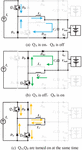
The topology of the low-voltage charging converter is shown in Figure 1. The front stage consists of DC/DC converters that have been optimized in previous designs. The back stage of the converter shown in Figure 1(a) utilizes a BSC circuit with switch dead-time as proposed in reference [1]. The back stage of the converter shown in Fig 1(b) is the proposed BSC circuit in this paper, which has no switch dead-time. Two inductors (L and L) are connected to the midpoint of the BSC full bridge. Where Vs represents the voltage on the DC side. V and V are the charging voltages of battery 1 and battery 2 respectively.
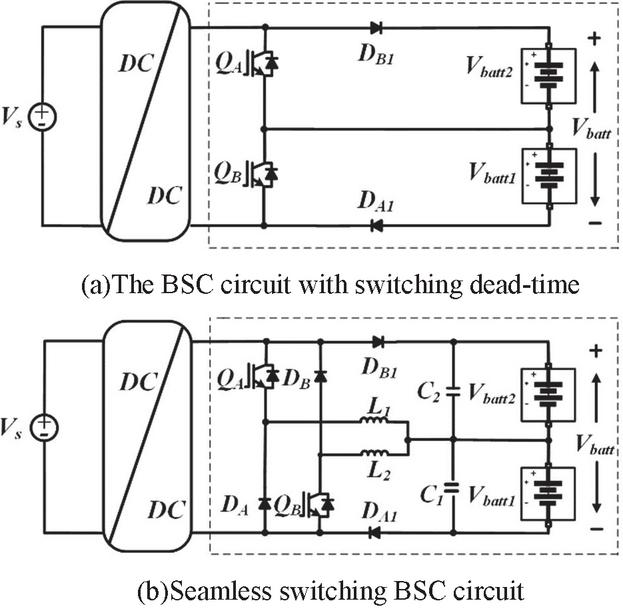
Figure 1 Low-voltage charging seamless switching converter topology.
2.2 Working Principle of Low Voltage Charging Seamless Switching Converter
To reduce the voltage across the secondary winding of the transformer, the BSC circuit is used to alternate between charging battery 1 and battery 2. The converter operates in two modes: battery charging mode and switching mode. We will make the ensuing postulates: (1) Disregard all unlisted parasitic elements that are not shown in Figure 2. (2) V, which represents the battery voltage, stays unchanged during the entire switching cycle.
(1) Charging mode
During the charging mode, the circuit’s equivalent model is illustrated in Figure 2(a) and 2(b), where Is represents the current input to the BSC circuit from the front stage.
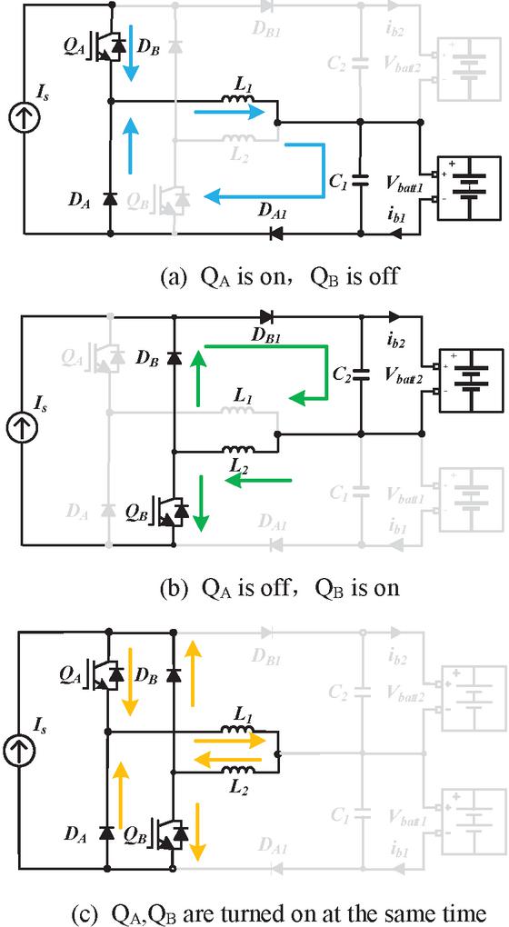
Figure 2 Equivalent circuit diagram in charging mode.
When Q is conducting and Q is turned off, the circuit’s equivalent representation, depicted in Figure 2(a) is established. The current flows through Q, sequentially passing through inductor L, capacitor C, V, diode D, and D, completing the charging of battery 1. When the current through Q is Is, based on the static characteristics curve of the IGBT, the conducting voltage U of the IGBT (Q)at this time can be obtained. By referring to the current-voltage characteristics curve of diode D, the current flowing through diode D at this time is I. Based on the above, the charging voltage of battery 1 at this time is:
| (1) |
When Q is turned off and Q is conducting, the circuit’s equivalent representation, depicted in Figure 2(b), is established. The current flows through Q, sequentially passing through diode D, diode D, capacitor C, and inductor L, completing the charging of battery 2. Similarly, the charging process for battery 2 is symmetric to that of battery 1. Therefore, the charging voltage of battery 2 can be obtained as:
| (2) |
(2) Switching mode
The innovation points of seamless switching technology in the 800V charging domain primarily focus on enhancing the continuity of the charging process and improving user experience. This technology allows electric vehicles to undergo seamless transitions during BSC circuit charging, reducing waiting times and enhancing the convenience of charging for users. When transitioning from charging battery 1 to charging battery 2, the converter operates in switching mode. The improved BSC converter allows for simultaneous conduction of Q and Q switches without the need for a dead-time setting. It operates in the overlapping region, as shown in Figure 2(c). During this time, the current rate of change is limited by the current-limiting inductor and stray inductances. The current is sustained by diodes D and D, facilitating a seamless transition from charging battery 1 to charging battery 2. The 400V DC/DC converter in the front stage does not need to be turned off. The voltage stress on the secondary side diodes (D–D) remains at V/2, as shown in Figure 3. This resolves the issue of frequent start-stop cycles in the 400V DC/DC converter caused by the switch dead-time in the BSC, thus improving charging reliability and energy utilization efficiency.
3 Control Strategy
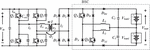
In order to validate the feasibility of the proposed BSC circuit seamless switching technology, we have chosen a phase-shifted full bridge converter as the front-stage DC/DC converter, as shown in Figure 3. The phase-shifted full bridge converter has a stable output voltage and flexible control strategies, making it widely used in DC/DC converters for electric vehicles.
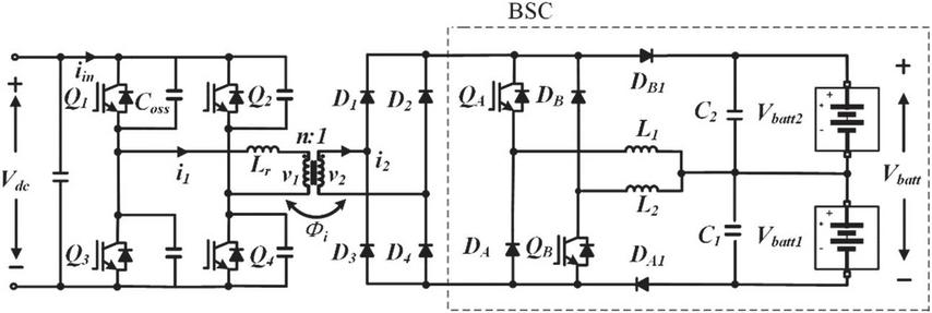
Figure 3 Low voltage charging seamless switching converter.
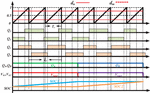
The low-voltage charging seamless switching converter adopts a dual-modulation scheme based on a sawtooth carrier wave, as shown in Figure 4. Q–Q represent the drive signals used to control the insulated gate bipolar transistors (IGBTs) in the corresponding H-bridge. The switching period Ts of the IGBTs is twice the carrier period Tc. The drive signals Q and Q for the rear-end BSC have a much longer switching period than T.
Let d be the duty cycle of the converter. Then, d and d can be expressed as
| (3) |
The phase-shift time can be expressed as:
| (4) |
Controlling the phase-shift time to adjust the output voltage and achieve a stable battery charging voltage is a common control strategy. In the low-voltage charging seamless switching converter, the main waveforms are shown in Figure 4.
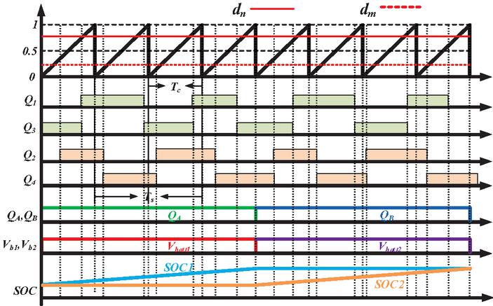
Figure 4 Dual modulation wave modulation based on sawtooth.
4 Key Parameter Design
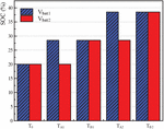
Due to the hard-switching nature of the Q and Q switches in the BSC circuit, their frequencies need to be designed independently of the main switches Q–Q in order to minimize switch losses. Despite Q and Q operating at a switch frequency f, it has no bearing on the balance of the charging process of the batteries over the whole time period during which charging occurs, The distinction between V and V within the BSC switching period increases as the switch frequency f decreases. Therefore, during the battery charging process, in crafting the design for the switch frequency, denoted as f, due consideration must be given to preventing over-discharge of the battery’s initial State of Charge (SOC) when under operational load conditions.
Figure 5 shows the battery SOC based on the switching of Q and Q when the battery is being charged. At the initial moment T, the SOC values of V and V are the same. During the time period T, Q conducts and charges V, causing its SOC to increase while V maintains its original SOC. In the time period T, Q conducts and charges V, causing its SOC to increase while V maintains its original SOC. The alternating charging of V and V achieves SOC balance.
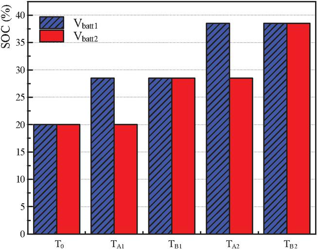
Figure 5 Battery SOC based on Q and Q exchange.
Beyond the previously outlined factors, the formulation of switch frequencies for Q and Q must also incorporate the Depth of Discharge (DOD) of the battery, a metric reflecting the proportion of total capacity discharged. Typically, a reduced DOD contributes to a prolonged battery life, whereas a greater DOD shortens it. A decrease in fB amplifies the DOD, thereby diminishing battery longevity, as the disparity between V and V intensifies over the charging duration during the discharge phase. Therefore, when determining the appropriate switch frequency, it is necessary to balance the circuit’s power consumption and the battery’s lifespan.
5 Loss Analysis
First, let me analyze the power losses of the components in the BSC circuit at a rated power of 1kW, and explain the theoretical calculation process.
The comprehensive switching operation of the IGBT demonstrates inherently non-linear behavior. The research on the switching losses of the IGBT mainly involves establishing the physical model of the IGBT or deriving formulas to calculate the losses. In this paper, we shall employ the loss computation methodology as graciously provided by Infineon’s authoritative online platform. The losses of the IGBT in the BSC circuit mainly consist of switching losses (P) and conduction losses (P). Since the switching frequency of Q and Q is low, the power losses of Q and Q are primarily conduction losses. The conduction losses of the IGBT can be calculated as follows:
| (5) |
u signifies the the voltage across the collector and emitter terminals of the IGBT when in the conductive state; r denotes the forward resistance during conduction bridging the collector-emitter junction points; i is the current coursing through the collector-emitter path; N represents the tally of IGBT units employed.
One may locate the collector-emitter voltage within the technical specifications of the IGW60T120 IGBT model. The same method can also be used to analyze the anti parallel diodes of all IGBTs in Figure 3, as illustrated subsequently:
| (6) |
The losses of the diode can be divided into conduction loss (P), recovery loss (P), and switching loss (P), which can be calculated using the following formulas:
| (7) | |
| (8) | |
| (9) |
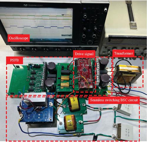
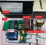
Figure 6 Experimental prototype.
| Parameter | Numeric | Description |
| V | 400 V | DC input voltage |
| V | 400 V | Battery 1 charging voltage |
| V | 400 V | Battery 1 charging voltage |
| N | 18:17 | Transformer ratio |
| 10 kHz | PSFB switching frequency | |
| 10 Hz | BSC circuit switching frequency | |
| C | 20 uF | Filter capacitor |
| L | 3 uH | Resonant Inductor |
| L | 1 mH | Filter Inductor |
Where I represents the average current, V is the reverse recovery voltage, V is the mean current-induced forward voltage decrement, and I is the maximum reverse recovery current. The aggregate diode loss can be articulated as:
| (10) |
The losses of the output filter capacitor are mainly caused by the fluctuating current traversing the capacitor’s equivalent series resistance (ESR). This converter employs an MKP-C4BT type filter capacitor with a capacitance of 20F. In the datasheet, the ESR is given as 1.710 . Therefore, the calculation for the filter capacitor (P) loss can be expressed as:
| (11) |
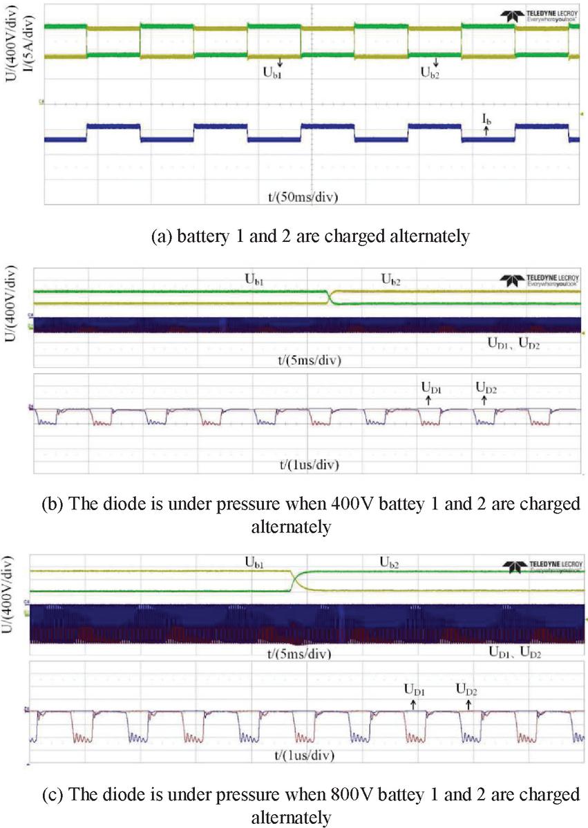
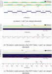
Figure 7 Experimental waveform.
The losses of the output inductor are mainly caused by the DC resistance (DCR) and the AC resistance (ACR) of the inductor coil. For a filter inductance with a value of 1mH and a switching frequency of 10Hz, with a DCR of 6.2810 , the loss of the filter inductor (P) can be calculated as:
| (12) |
The total power loss (P) in the BSC circuit can be represented as:
| (13) |
6 Experimental Verification
To validate the feasibility and superiority of the proposed 800V low-voltage seamless switching technology, an experimental prototype was constructed as shown in Figure 6. The main parameters of the prototype are listed in Table 1.
In the charging mode, the measured shapes of the charging voltage and current waveforms for battery 1 and battery 2 are shown in Figure 7(a). It can be observed that battery 1 and battery 2 achieve seamless alternating charging. As shown in Figure 7(b) and 7(c), during the charging process of the 400V and 800V batteries, the voltage across the secondary-side diodes is clamped to V/2. There is no need to set a dead time during the transition from charging battery 1 to charging battery 2, which improves the reliability of the charging process. Moreover, this converter exhibits reduced voltage stress across all DC/DC and BSC components, leading to a decrease in conduction losses.
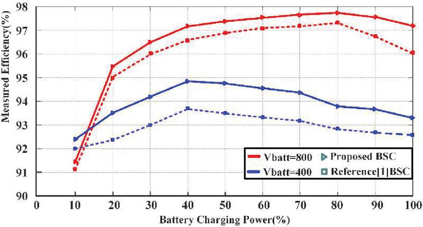
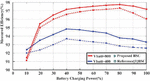
Figure 8 Comparison of efficiency curves.
By comparing the power losses between the BSC circuit with dead time from reference [1] and the BSC circuit without dead time proposed in this paper, the efficiency curves are obtained as shown in Figure 8. It can be observed that, under different voltage charging powers, regardless of whether it is under 800V or 400V voltage conditions, the efficiency of the topology presented in this paper is higher than the efficiency of the topology in reference [1].
7 Conclusion
A fresh approach to low-voltage charging seamless switching technique is presented in this document that addresses the dead-time issue in the BSC circuit mentioned in reference [1], enabling seamless switching for high-voltage battery charging. By eliminating the dead-time in the secondary stage, the overall conduction losses of the converter are reduced. Additionally, decoupling the switching frequency of the BSC circuit from the primary DC/DC converter helps minimize the switching losses in the BSC circuit. Compared to traditional converters, this converter exhibits lower voltage stress on the secondary side components, resulting in reduced conduction losses and improved efficiency. The seamless charging mode ensures a smoother charging process, reducing instantaneous power fluctuations. This optimization aids in balancing power demand and enhances grid stability.
Acknowledgements
This project is funded by the science and technology project of Jilin Electric Power Research Institute Co., Ltd., and the project number is KY-GS-23-01-01. The project name is the research on the flexible regulation and load side response strategy of the new distribution network edge collaborative voltage of the Electric Power Research Institute. I sincerely thank them for their support and contributions.
References
[1] J.-Y. Kim, B.-S. Lee, and D.-H. Kwon, “Low Voltage Charging Technique for Electric Vehicles With 800 V Battery,” IEEE Transactions on Industrial Electronics, vol. 69, no. 8, pp. 7890–7896, Aug. 2022.
[2] C. Jung, “Power up with 800-V systems: The benefits ofupgrading voltage power for battery-electric passenger vehicles,” IEEE Electrif. Mag, vol. 5, no. 1, pp. 53–58, Mar. 2017.
[3] I. Aghabali, J. Bauman, and A. Emadi, “Analysis of auxiliary power unit and charging for an 800V electric vehicle,” in Proc. IEEE Transp. Electrif. Conf. Expo, Jun. 2019, pp. 1–6.
[4] H. Wang and Z. Li, “A PWM LLC type resonant converter adapted to wide output range in PEV charging applications,” IEEE Trans. Power Electron, vol. 33, no. 5, pp. 3791–3801, May 2018.
[5] H. N. Tran, T. -T. Le, and H. Jeong, “High Power Density DC-DC Converter for 800V Fuel Cell Electric Vehicles,” IEEE 12th Energy Conversion Congress & Exposition, Singapore, 2021, pp. 2224–2228.
[6] Allca-Pekarovic, P. J. Kollmeyer, and P. Mahvelatishamsabadi, “Comparison of IGBT and SiC Inverter Loss for 400V and 800V DC Bus Electric Vehicle Drivetrains,” IEEE Energy Conversion Congress and Exposition, Detroit, MI, USA, 2020, pp. 6338–6344.
[7] Vraèar, Darko, Pejoviæ, Predrag. “Active-clamped flyback DC-DC converter in an 800V application: Design notes and control aspects,” Journal of Electrical Engineering, vol. 73, no. 4, 2022, pp.237–247.
[8] Bertino, D. de Simone and L. Piegari, “Design and operation of a fail-operational 5kW 800V-12V DC-DC converter,” European Conference on Power Electronics and Applications, Genova, Italy, 2019, pp. 1–10.
[9] Aghabali, J. Bauman and A. Emadi, “Analysis of Auxiliary Power Unit and Charging for an 800V Electric Vehicle,” IEEE Transportation Electrification Conference and Expo, Detroit, MI, USA, 2019, pp. 1–6.
[10] C. Lim, Y. Jeong, and G. Moon, “Phase-shifted full-bridge DC-DC converter with high efficiency and high power density using center-tapped clamp circuit for battery charging in electric vehicles,” IEEE Trans. Power Electron., vol. 34, no. 11, pp. 10945–10959, Nov. 2019.
[11] M. Abbasi and J. Lam, “An SiC-based AC/DC CCM bridgeless onboard EVchargerwith coupled active voltage doubler rectifiers for 800-V battery systems,” IEEE Appl. Power Electron. Conf. Expo, Mar. 2020, pp. 905–910.
[12] K. Kim, J. Han, B. Lee, and G. Moon, “High-efficiency three-level DC-DC converter with reduced circulating current and rectifier voltage stress,” IEEE Trans. Power Electron, vol. 35, no. 3, pp. 2668–2679.
[13] Z. Guo, K. Sun and L. Zhang, “Analysis and Evaluation of Dual Half-Bridge Cascaded Three-Level DC–DC Converter for Reducing Circulating Current Loss,” IEEE Journal of Emerging and Selected Topics in Power Electronics, vol. 5, no. 1, March 2017, pp. 351–362.
[14] H. Haga and F. Kurokawa, “Modulationmethod ofa full-bridge three-level LLC resonant converter for battery charger of electrical vehicles,” IEEE Trans. Power Electron, vol. 32, no. 4, pp. 2498–2507, Apr. 2017.
[15] L. A. D. Ta, N. D. Dao and D. -C. Lee, “High-Efficiency Hybrid LLC Resonant Converter for On-Board Chargers of Plug-In Electric Vehicles,” IEEE Transactions on Power Electronics, vol. 35, no. 8, pp. 8324–8334, Aug. 2020.
[16] Nazerian, R. Yu, Q. Huang, M. Heydari, H. S. Rizi and A. Q. Huang, “High Efficiency, High Power Density 10kW Flying Capacitor Converter Based on 650V GaN for 800V EV Applications,” IEEE Energy Conversion Congress and Exposition , Nashville, TN, USA, 2023, pp. 1863–1869.
[17] N. Langmaack, G. Tareilus, G. Bremer, and M. Henke, “Transformerlessonboard charger for electric vehicles with 800 V power system,” IEEE 13th Int. Conf. Power Electron. Drive Syst, Jul. 2019, pp. 1–5.
[18] S. H. Lee, B. Lee, D. Kwon, J. Ahn, and J. Kim, “Two-mode low-voltage DC/DC converter with high and wide input voltage range,” IEEE Trans. Ind. Electron, vol. 68, no. 12, pp. 12088–12099, Dec. 2021.
[19] B. Kim, K. Kim, and S. Choi, “A 800V/14V soft-switched converter with low-voltage rating of switch for xEV applications,” in Proc. Int. Power Electron. Conf, May 2018, pp. 256–260.
[20] Mishra, S., Das, D., & Paul, S. (2010). Active Loss Allocation Systems in Radial Distribution Systems. Cogeneration & Distributed Generation Journal, 25(3), 26–43.
[21] Ramana, T., Ganesh, V., & Sivanagaraju, S. (2010). Distributed Generator Placement And Sizing in Unbalanced Radial Distribution System. Cogeneration & Distributed Generation Journal, 25(1), 52–71.
[22] Kong, X., Zhang, Z., & Yin, X. (2015). Fault Current Study of Inverter Interfaced Distributed Generators. Distributed Generation & Alternative Energy Journal, 30(3), 6–26.
Biographies
Yuze Fu, female, born in 1978, Ph. She has presided over and participated in one national scientific research project, three provincial and ministerial scientific research projects, and five horizontal projects. Research Direction Power System Fault Diagnosis and Load Prediction Now affiliated with Northeast Power University.
Zhe Shi, Male, Dalian, Liaoning Province. His research interests include revenue allocation of coupled systems within the power market.
Cong Wang, male, is currently a master’s degree candidate in Electrical Engineering at Northeast Electric Power University. His research focuses on electricity markets and low-carbon optimization operation of power systems.
Zhenxu Ma, male, obtained a master’s degree in Power System and Automation from Tsinghua University in 2000. His main research interests include planning, preliminary work, and investment in primary distribution networks.
Ruifeng Li, male, is currently a master’s degree candidate in Electrical Engineering at Northeast Electric Power University. His research focuses on electricity markets and low-carbon optimization operation of power systems.
Dongbo Guo, Ph.D. His main research direction is power systems and their automation.
Distributed Generation & Alternative Energy Journal, Vol. 39_5, 1097–1114.
doi: 10.13052/dgaej2156-3306.3957
© 2024 River Publishers