Improved Performance of Dual Active Bridge Converter using Particle Swarm Optimization based Phase Shift Modulation for EV Application
Khurshid Ul Haq1,*, Farhad Ilahi Bakhsh1 and Obbu Chandra Sekhar
1Electrical Engineering Department, National Institute of Technology Srinagar, J&K India
2Electrical Engineering Department, National Institute of Technology Delhi, India
E-mail: khurshid_10phd19@nitsri.ac.in
*Corresponding Author
Received 20 March 2025; Accepted 11 April 2025
Abstract
The five-level dual active bridge (FLDAB) topology is recently presented to suppress the harmonic content in the high frequency link (HFL) of DC-DC converter. However, the conventional FLDAB topology requires additional four diodes and one switch for the generation of five-level at the output. These four diodes and one switch cause losses in the system and hence the efficiency of the system decreases. Keeping the drawbacks of conventional FLDAB topology in view, this paper presents a novel FLDAB topology with the lower component count i.e., two switches only. The proposed FLDAB topology based DC-DC converter implements PSO based modulation for electric vehicle application. This paper presents a detailed analysis of the proposed FLDAB topology. Further, the analysis involves a comparative evaluation against conventional FLDAB topology. The comparative results shows that the proposed topology produces lesser harmonics in the HFL of the DC-DC converter and it is more efficient than the conventional FLDAB topology. Thus presenting a promising and improved solution for DC-DC converters in electric vehicle application. The OPAL-RT hardware-in-loop emulator validates the obtained results.
Keywords: Multilevel dual active bridge (MLDAB), high frequency link (HFL), total harmonic distortion (THD), particle swarm optimization (PSO) algorithm.
1 Introduction
The need for awareness of environmental issues and strict rules to reduce greenhouse gas emissions have accelerated the push for environmental friendly modes of transportation. Consequently, the automotive industry is experiencing a notable shift from conventional internal combustion engine based vehicle technology to electrification. The growing adoption of electric vehicles (EVs) and advancements in charging infrastructure drive this transition [1]. However, the lack of sufficient charging infrastructure and the lack to meet the international charging standards not only restrain the expansion of EVs but also increase the quantity of charging infrastructure with subpar performance [2, 3]. The majority of existing charging methods do not meet the international requirements. Low power factor and high total harmonic distortion (THD) are all indicators of poor performance [4]. Increasing the need for a universal charging system for all EVs, implementation of a number of different single stage and two stage charger topologies for EVs has been the subject of research [5, 6]. As in current chargers the performance metrics of interest include the input power factor, distortion factor, displacement factor and charger efficiency, all degrade when diode bridge rectifier is used in conjunction with a dc-link capacitor. Generally, better performance characteristics have been demonstrated for two-stage designs. To enhance the power quality of an AC-DC conversion system, active power factor correction (APFC) circuits based on boost converters have gained widespread adoption in medium to high power applications [7, 8]. However, their usefulness was constrained by a few factors, prompting researchers to look for alternatives. Therefore, a number of APFC implementations using a variety of converters deriving from the buck-boost topology as in references [9, 10]. However, their application is constrained at low to medium power levels because of the high current stress, huge filter demand and more number of devices being used. The use of interleaved cells appears favourable at high power application as mentioned in [11, 12]. Nevertheless, the increase in the large filter requirement and increase in device count persists.
It is crucial to have power converters for EV applications that have galvanic isolation and the bidirectional flow of power. Multiple configurations of isolated bidirectional DC-DC converters (IBDCs) are possible [13–15]. Due to its inherent ability of soft switching without using any auxiliary components, the DAB converter is the best IBDC for power applications like battery management systems, EVs, solid-state transformers and DC distribution system interface. Many indices frequently impact the performance of the DAB converter, including increased current stress on the HFL device due to harmonics in the inductor current. The harmonics also cause the HFT and the devices to overheat, hence decrease in efficiency of the converter. The achievement of high efficiency and reliability in DAB can be attained by making modifications to the performance indices via the modulation schemes and circuit architecture [16]. Single phase shift (SPS) modulation is widely recognized as the most prevalent modulation technique. However in SPS modulation technique, the converter experiences significant current stress and limited soft-switching range [17]. In order to address these challenges, researchers have developed different modulation techniques including extended phase shift (EPS) modulation [18], dual-phase shift (DPS) modulation [19], and triple-phase shift (TPS) modulation [20]. In addition to the aforementioned modulation systems, there are alternative methods such as hybrid modulation as discussed in [21]. However, these techniques produce much harmonics in the HFL of the DAB converter. Therefore, the efficiency of the converter reduces.
In order to reduce the THD of the HFL current waveform, multilevel topologies are used by different researchers at the either end of the DAB converter. In [22], the authors provide a solution to operate multilevel DAB converter consists of neutral point clamped configuration having different levels. Further, in order to reduce the inductor current THD and to achieve this, an additional four active switches are employed to generate a five-level voltage waveform which reduces the efficiency of the system [23]. A modulation technique with additional degrees of freedom used to minimize harmonics. However, this improvement required the addition of four extra components on both sides of the converter [24]. Further, in [25] a transistor clamped FLDAB converter is proposed with voltages of two and five level due to three degrees of freedom which improves its ability to regulate power flow, and the inductor current THD reduces. Also the performance evaluation of converter topology, incorporating five voltage levels on both sides of the HFT, therefore diminishing the inductor current harmonics [26]. Further, the QPS-modulation based topology, incorporating auxiliary switch. This design aids in mitigating the inductor current harmonics [27]. However for generating five-level in [25–27], additional components (switches & diodes) are required, therefore compromising their efficiency. Keeping the above mentioned drawback in view, the authors have presented a novel FLDAB topology using PSO based modulation technique for EV application. This study outlines the following primary contributions:
• A novel FLDAB converter topology using PSO algorithm based modulation technique has been developed.
• The performance of the proposed FLDAB converter using PSO based modulation technique and conventional FLDAB converter with QPS scheme has been compared.
• The comparative results shows that the proposed PSO modulation based converter produces lesser harmonics in the HFL of the DC-DC converter and it is more efficient than the conventional FLDAB converter.
• The results achieved are validated by OPAL-RT emulator.
The following sections organize the remainder of this work as follows:
Sections 2 and 3 illustrates the conventional converter and its control strategy. Sections 4 and 5, deals with topology and the control strategy of the proposed FLDAB converter using PSO based modulation. Section 6, deals with the simulation as well as real time results. Section 7, deals with the comparison illustration. Finally, a conclusion is drawn in Section 8.
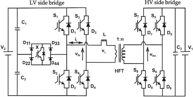
Figure 1 Schematic of the conventional converter.
2 Conventional Topology
HFT connects both the HV and LV side bridges. The four active switches () integrated with antiparallel diode (), a bidirectional auxiliary switch (X) along with four diodes ), complete the LV side-bridge. The four active switches () with incorporated antiparallel diodes () complete the HV side bridge. and denote the AC voltages of the bridges. The turns ratio of the HFT is represented by ’ and the capacitances are , , and . ’ and ’ denote the inductor voltage and current respectively as illustrated in Figure 1.
3 Control Strategy of Conventional Converter
Figures 2 and 3, depict the operation of the conventional MLDAB converter. To have desired voltage levels in both the modes of operation it is essential to adjust the switching status in the HV and LV side bridge configurations as below, The G2V operation at different instants is illustrated in Figure 2(a–g). The turn-on of switches and in HV side bridge. In the LV side bridge, and switches turn on during the time interval from to as depicted in Figure 2(a). The turn-on of switches and in HV side bridge. In the LV side bridge, and switches turn on during the time interval from to as depicted in Figure 2(b). The turn-on of switches and in HV side bridge. In the LV side bridge, and switches turn on during the time interval as shown in Figure 2(c). The turn-on of switches and in HV side bridge. In the LV side bridge, and switches turn on during the time interval from to as depicted in Figure 2(d). The turn-on of switches and in HV side bridge. In the LV side bridge, and switches turn on during the time interval from to as depicted in Figure 2(e). The turn-on of switches and in HV side bridge. In the LV side bridge, and switches turn on during the time interval from to as depicted in Figure 2(f). The turn-on of switches and in HV side bridge. In the LV side bridge, and switches turn on during the time interval from to as depicted in Figure 2(g). Furthermore, for the forward mode of operation the switching states as shown in Table 1, has been made according to the above mentioned operation.
The V2G operation at different instants is illustrated in Figure 3(a–g). The turn-on of switches and in HV side bridge. In the LV side bridge, and switches turn on during the time interval from to as depicted in Figure 3(a). The turn-on of switches and in HV side bridge. In the LV side bridge, and switches turn on during the time interval from to as depicted in Figure 3(b). The turn-on of switches and in HV side bridge. In the LV side bridge, and switches turn on as shown in Figure 3(c). The turn-on of switches and in HV side bridge. In the LV side bridge, and switches turn on during the time interval from to as depicted in Figure 3(d). The turn-on of switches and in HV side bridge. In the LV side bridge, and switches turn on during the time interval from to as depicted in Figure 3(e). The turn-on of switches and in HV side bridge. In the LV side bridge, and switches turn on during the time interval from to as depicted at the last of in Figure 3(f). The turn-on of switches and in HV side bridge. In the LV side bridge, and switches turn on during the time interval from to as depicted at the last. Also, the states of switches as shown in Table 2 is made accordingly.
Table 1 G2V states of switches of conventional converter
| Switching States | Modes | |||||||||||||
| 1 | 2 | 3 | 4 | 5 | 6 | 7 | 8 | 9 | 10 | 11 | 12 | 13 | 14 | |
| 1 | 0 | 1 | 1 | 0 | 0 | 0 | 0 | 0 | 0 | 0 | 0 | 0 | 1 | |
| 0 | 0 | 0 | 0 | 0 | 0 | 1 | 1 | 0 | 1 | 1 | 0 | 0 | 0 | |
| 1 | 0 | 0 | 0 | 0 | 0 | 0 | 0 | 1 | 1 | 1 | 1 | 1 | 1 | |
| 0 | 1 | 1 | 1 | 1 | 1 | 1 | 1 | 0 | 0 | 0 | 0 | 0 | 0 | |
| 1 | 1 | 1 | 1 | 1 | 0 | 0 | 0 | 0 | 0 | 0 | 0 | 1 | 1 | |
| 0 | 0 | 0 | 0 | 0 | 1 | 1 | 1 | 1 | 1 | 1 | 1 | 0 | 0 | |
| 0 | 0 | 0 | 1 | 1 | 1 | 1 | 1 | 1 | 1 | 0 | 0 | 0 | 0 | |
| 1 | 1 | 1 | 0 | 0 | 0 | 0 | 0 | 0 | 0 | 1 | 1 | 1 | 1 | |
| X | 0 | 1 | 0 | 0 | 1 | 1 | 0 | 0 | 1 | 0 | 0 | 1 | 1 | 0 |
Table 2 V2G states of switches of conventional converter
| Switching States | Modes | |||||||||||||
| 1 | 2 | 3 | 4 | 5 | 6 | 7 | 8 | 9 | 10 | 11 | 12 | 13 | 14 | |
| 1 | 0 | 0 | 0 | 0 | 0 | 0 | 0 | 0 | 0 | 1 | 1 | 0 | 1 | |
| 0 | 0 | 0 | 1 | 1 | 0 | 1 | 1 | 0 | 0 | 0 | 0 | 0 | 0 | |
| 1 | 1 | 1 | 1 | 1 | 1 | 0 | 0 | 0 | 0 | 0 | 0 | 0 | 0 | |
| 0 | 0 | 0 | 0 | 0 | 0 | 1 | 1 | 1 | 1 | 1 | 1 | 1 | 0 | |
| 1 | 1 | 0 | 0 | 0 | 0 | 0 | 0 | 0 | 1 | 1 | 1 | 1 | 1 | |
| 0 | 0 | 1 | 1 | 1 | 1 | 1 | 1 | 1 | 0 | 0 | 0 | 0 | 0 | |
| 0 | 0 | 0 | 0 | 1 | 1 | 1 | 1 | 1 | 1 | 1 | 0 | 0 | 0 | |
| 1 | 1 | 1 | 1 | 0 | 0 | 0 | 0 | 0 | 0 | 0 | 1 | 1 | 1 | |
| X | 0 | 1 | 1 | 0 | 0 | 1 | 0 | 0 | 1 | 1 | 0 | 0 | 1 | 0 |
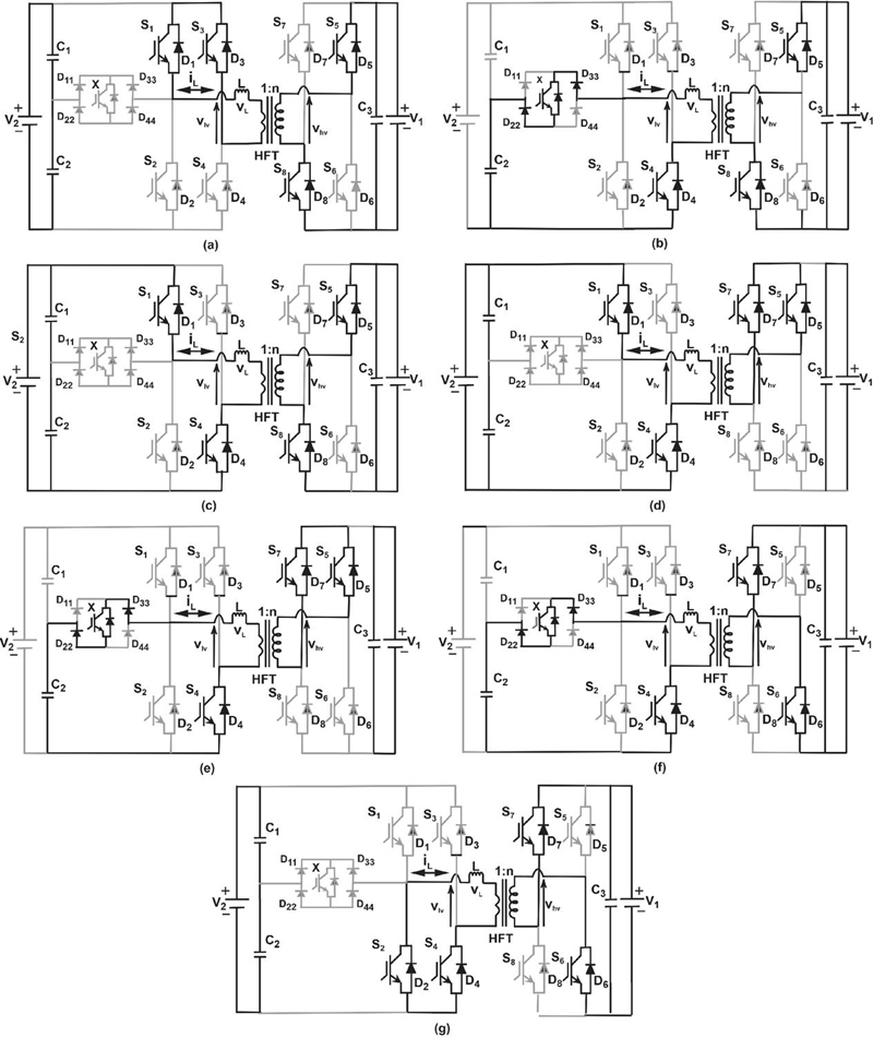
Figure 2 G2V operation of conventional converter.
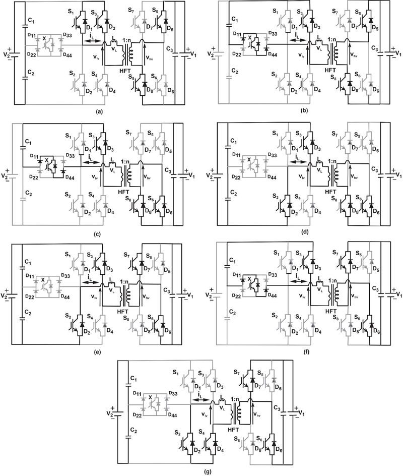
Figure 3 V2G operation of conventional converter.
4 Proposed FLDAB Converter
HFT connects both the HV and LV side bridges. The four active switches () integrated with antiparallel diodes (), and a bidirectional auxiliary switches () connects one of the midpoints of the H-bridge leg to the capacitor leg, completing the LV side bridge. The auxiliary switch consists of the two active switch () connected in antiparallel to each other. Four active switches () and integrated antiparallel diodes () form the HV side bridge. and denote the voltages of the bridges. The turns ratio of the HFT is represented by ’ and the capacitances are , , and . ’ and ’denote the inductor voltage and current respectively as illustrated in Figure 4.
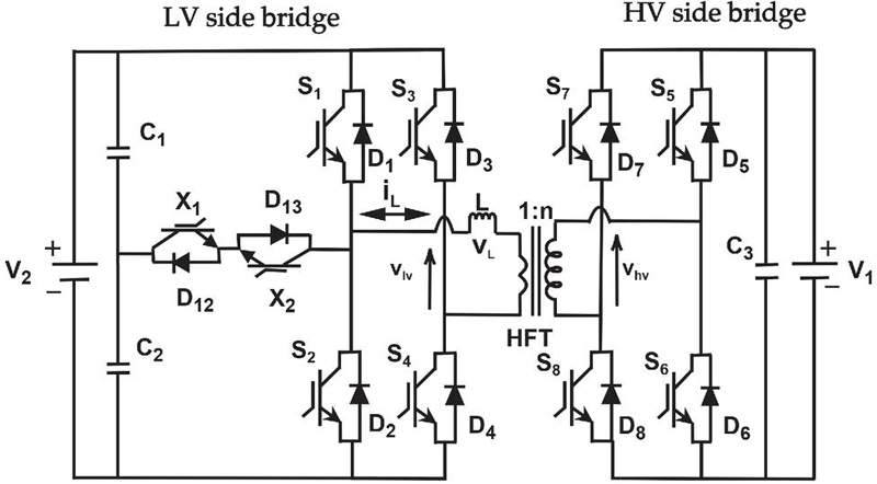
Figure 4 Schematic of proposed converter.
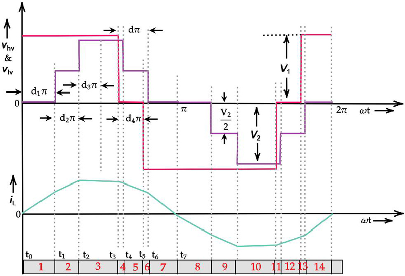
Figure 5 Proposed G2V operating waveforms.
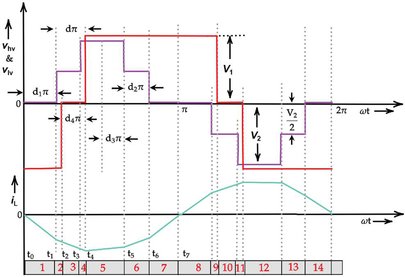
Figure 6 Proposed V2G operating waveforms.
5 Proposed PSO Based Modulation Control Strategy of FLDAB Converter
5.1 Operating Principle of Proposed FLDAB Converter
Figures 5 and 6, depict the operation of the proposed FLDAB converter. To have desired voltage levels in both the modes of operation it is essential to adjust the switching status in the HV and LV side bridge configurations as below, The G2V operation at different instants is illustrated in Figure 7. The turn-on of switches and in HV side bridge. In the LV side bridge, and switches turn on during the time interval from to as depicted in Figure 7(a). HV Side and LV side voltages are and respectively. Current increases and is expressed as,
| (1) |
The turn-on of switches and in HV side bridge. In the LV side bridge, and switches turn on during the time interval from to as depicted in Figure 7(b). HV Side and LV side voltages are and respectively. Current increases and is expressed as,
| (2) |
The turn-on of switches and in HV side bridge. In the LV side bridge, and switches turn on as shown in Figure 7(c). HV Side and LV side voltages are and respectively. Current increases and is expressed as,
| (3) |
The turn-on of switches and in HV side bridge. In the LV side bridge, and switches turn on during the time interval from to as depicted in Figure 7(d). HV Side and LV side voltages are and respectively. Current decreases and is expressed as,
| (4) |
The turn-on of switches and in HV side bridge. In the LV side bridge, and switches turn on during the time interval from to as depicted in Figure 7(e). HV Side and LV side voltages are and respectively. Current decreases and is expressed as,
| (5) |
The turn-on of switches and in HV side bridge. In the LV side bridge, and switches turn on during the time interval from to as depicted in Figure 7(f). HV Side and LV side voltages are and respectively. Current decreases and is expressed as,
| (6) |
The turn-on of switches and in HV side bridge. In the LV side bridge, and switches turn on during the time interval from to as depicted in Figure 7(g). HV Side and LV side voltages are and respectively. Current decreases and is expressed as,
| (7) |
Furthermore, for the forward mode of operation the switching states as shown in Table 3, has been made according to the above mentioned operation. The V2G operation at different instants is illustrated in Figure 8(a–g). The turn-on of switches and in HV side bridge. In the LV side bridge, and switches turn on during the time interval from to as depicted in Figure 8(a). HV Side and LV side voltages are and respectively. Current increases in reverse direction and is expressed as,
| (8) |
The turn-on of switches and in HV side bridge. In the LV side bridge, and switches turn on during the time interval from to as depicted in Figure 8(b). HV Side and LV side voltages are and respectively. Current increases in reverse direction and is expressed as,
| (9) |
The turn-on of switches and in HV side bridge. In the LV side bridge, and switches turn on as shown in Figure 8(c). HV Side and LV side voltages are and respectively. Current increases in reverse direction and is expressed as,
| (10) |
The turn-on of switches and in HV side bridge. In the LV side bridge, and switches turn on during the time interval from to as depicted in Figure 8(d). HV Side and LV side voltages are and respectively. Current increases in reverse direction and is expressed as,
| (11) |
The turn-on of switches and in HV side bridge. In the LV side bridge, and switches turn on during the time interval from to as depicted in Figure 8(e). HV Side and LV side voltages are and respectively. Current decreases and is expressed as,
| (12) |
The turn-on of switches and in HV side bridge. In the LV side bridge, and switches turn on during the time interval from to as depicted in Figure 8(f). HV Side and LV side voltages are and respectively. Current decreases and is expressed as,
| (13) |
The turn-on of switches and in HV side bridge. In the LV side bridge, and switches turn on during the time interval from to as depicted in Figure 8(g). HV Side and LV side voltages are and respectively. Current decreases and is expressed as,
| (14) |
Furthermore, for reverse mode of operation the switching states as shown in Table 4 and has been carried out in accordance with the aforementioned operation.
Table 3 States of switches of proposed FLDAB converter using PSO based modulation for forward mode of operation
| Switching States | Modes | |||||||||||||
| 1 | 2 | 3 | 4 | 5 | 6 | 7 | 8 | 9 | 10 | 11 | 12 | 13 | 14 | |
| 1 | 0 | 1 | 1 | 0 | 0 | 0 | 0 | 0 | 0 | 0 | 0 | 0 | 1 | |
| 0 | 0 | 0 | 0 | 0 | 0 | 1 | 1 | 0 | 1 | 1 | 0 | 0 | 0 | |
| 1 | 0 | 0 | 0 | 0 | 0 | 0 | 0 | 1 | 1 | 1 | 1 | 1 | 1 | |
| 0 | 1 | 1 | 1 | 1 | 1 | 1 | 1 | 0 | 0 | 0 | 0 | 0 | 0 | |
| 1 | 1 | 1 | 1 | 1 | 0 | 0 | 0 | 0 | 0 | 0 | 0 | 1 | 1 | |
| 0 | 0 | 0 | 0 | 0 | 1 | 1 | 1 | 1 | 1 | 1 | 1 | 0 | 0 | |
| 0 | 0 | 0 | 1 | 1 | 1 | 1 | 1 | 1 | 1 | 0 | 0 | 0 | 0 | |
| 1 | 1 | 1 | 0 | 0 | 0 | 0 | 0 | 0 | 0 | 1 | 1 | 1 | 1 | |
| 0 | 0 | 0 | 0 | 0 | 0 | 0 | 0 | 1 | 0 | 0 | 1 | 1 | 0 | |
| 0 | 1 | 0 | 0 | 1 | 1 | 0 | 0 | 0 | 0 | 0 | 0 | 0 | 0 | |
Table 4 States of switches of proposed FLDAB converter using PSO based modulation for reverse mode of operation
| Switching States | Modes | |||||||||||||
| 1 | 2 | 3 | 4 | 5 | 6 | 7 | 8 | 9 | 10 | 11 | 12 | 13 | 14 | |
| 1 | 0 | 0 | 0 | 0 | 0 | 0 | 0 | 0 | 0 | 1 | 1 | 0 | 1 | |
| 0 | 0 | 0 | 1 | 1 | 0 | 1 | 1 | 0 | 0 | 0 | 0 | 0 | 0 | |
| 1 | 1 | 1 | 1 | 1 | 1 | 0 | 0 | 0 | 0 | 0 | 0 | 0 | 0 | |
| 0 | 0 | 0 | 0 | 0 | 0 | 1 | 1 | 1 | 1 | 1 | 1 | 1 | 0 | |
| 1 | 1 | 0 | 0 | 0 | 0 | 0 | 0 | 0 | 1 | 1 | 1 | 1 | 1 | |
| 0 | 0 | 1 | 1 | 1 | 1 | 1 | 1 | 1 | 0 | 0 | 0 | 0 | 0 | |
| 0 | 0 | 0 | 0 | 1 | 1 | 1 | 1 | 1 | 1 | 1 | 0 | 0 | 0 | |
| 1 | 1 | 1 | 1 | 0 | 0 | 0 | 0 | 0 | 0 | 0 | 1 | 1 | 1 | |
| 0 | 1 | 1 | 0 | 0 | 1 | 0 | 0 | 0 | 0 | 0 | 0 | 0 | 0 | |
| 0 | 0 | 0 | 0 | 0 | 0 | 0 | 0 | 1 | 1 | 0 | 0 | 1 | 0 | |
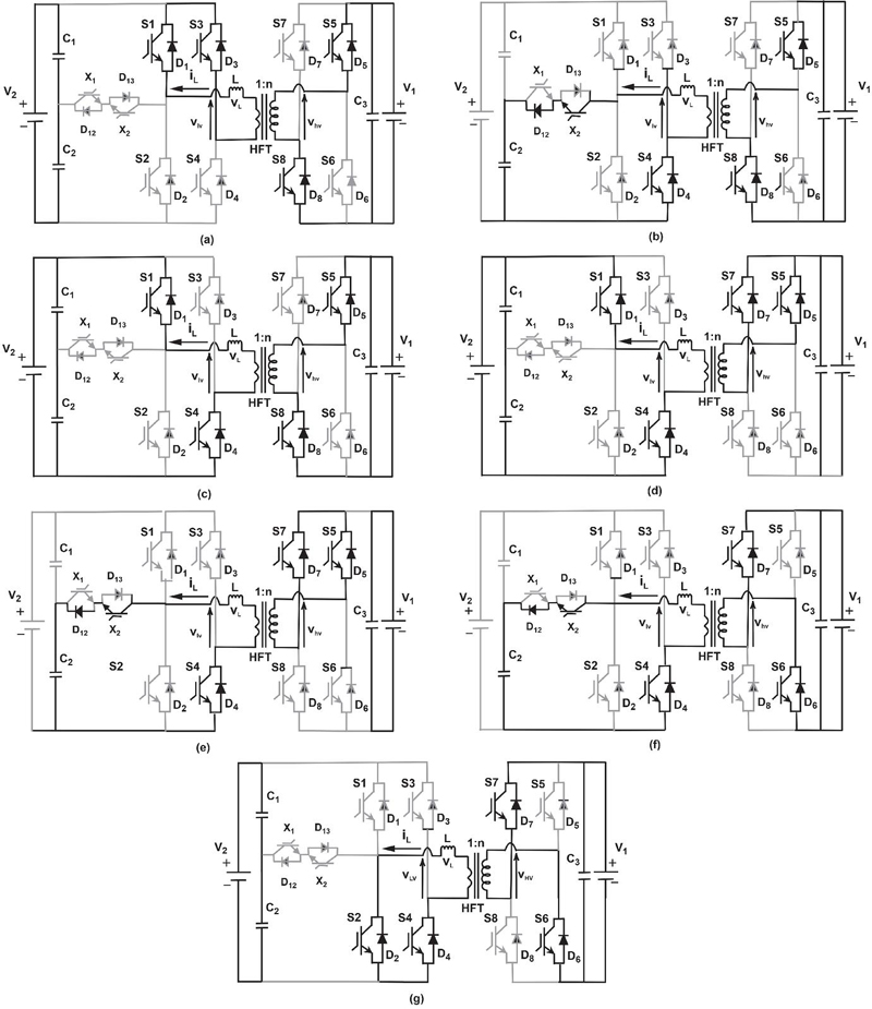
Figure 7 G2V operation of proposed modulation based FLDAB converter, whereas a) , b) , c) , d) , e) , f) and g) .
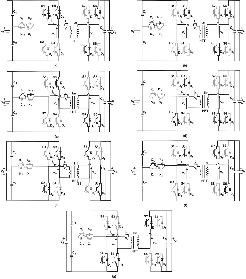
Figure 8 V2G operation of proposed modulation based FLDAB converter, whereas a) , b) , c) , d) , e) , f) and g) .
5.2 Harmonic Approach with PSO-Algorithm for Improved System Performance
Significant power loss in a system is attributed to harmonics, which are signals characterized by frequencies that are integer multiples of the fundamental frequency. The mitigation of harmonic content in inductor current is crucial due to its potential to decrease losses in high-frequency transformer (HFT), which play a vital role in the operation of the multi-level dual active bridge (MLDAB) system. The utilization of the Fourier series methodology offers a comprehensive equations. The voltage waveform denoted as has a square shape with three distinct levels and possesses the property of half-wave symmetry as shown in Figure 6. Because of the principle of half-wave symmetry, the coefficient is determined to be zero. Additionally, the coefficients and are also zero for values of n that are even. Consequently,
| (15) |
where;
From Figure 6, is 0 for the time interval and is for . Thus, on solving (15),
| (16) |
Likewise, the variable represents a square waveform consisting of five levels, exhibiting both odd and half-wave symmetry. Therefore, the values of and are both equal to 0 for all values of , whereas the value of is equal to 0 only for even values of and can be written as;
| (17) |
where;
From Figure 6, is 0 for time interval for and for . Thus, on solving (17),
| (18) |
where;
The inductor voltage is given as;
| (19) |
By performing integration, the expression for the inductor current as below;
| (20) |
As the average inductor current throughout a switching time is zero, it can be deduced that the inductor current at is equivalent to . By evaluating the expression , it is possible to determine the current flowing through the inductor using equation (20).
| (21) |
where,
From equation (21), the RMS current is represented as;
| (22) |
Harmonics cause significant power loss in the system. It is crucial to lower the harmonic content of inductor current, since doing so can lower HFT losses, which is an important component of the MLDAB. In order to seek a set of optimal operating points to reduce system loss and improve the efficiency of the DAB converter, PSO algorithm is adopted for system optimization. The rms inductor current, which is adopted as the objective function and finding a set of optimal combination of () to minimize the rms inductor current under constraints based on the operational principle of the proposed MLDAB converter are shown as follows;
| (23) |
Figure 9 illustrates the optimization flowchart. In the start stage, constraints as in equation (23), for the fitness function as in equation (22). After that, the PSO algorithm will conduct fitness evaluation, then update and as well as the velocity and position of particles. The termination condition for the PSO algorithm is based on the criteria. If the maximum iteration is reached. The system achieves the minimum RMS current. After that, optimal variables () are obtained and gate signals are generated.
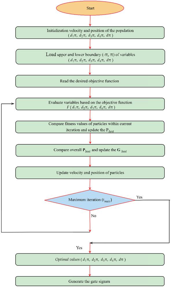
Figure 9 Flowchart of the proposed PSO algorithm.
PSO algorithm, in addition to its outstanding global search ability, it also features the merits of good robustness and fast computation speed and it is adopted in this article. The PSO algorithm mimics the random hunting behavior of birds. It first needs to initialize a swarm of randomly distributed particles in the n-dimensional search space. For the optimization problem in this article, since the position of each particle is determined by the combination of (). Each individual particle represents a potential optimal solution, which involves two characteristic indexes, position and velocity .
where the initial number of particles is defined as and are the position and velocity of the -th particle, respectively. The key of the PSO algorithm is the updating formulas of velocity and position for each individual particle.
where;
• is the iteration index.
• is the inertia weight, generally , reflecting the tendency of a particle to maintain its previous velocity.
• is the individual learning factor, generally . It reflects the tendency of a particle to approach the historical optimal position of individual Pxbest.
• is the swarm learning factor, generally . It reflects the tendency of particles to approach the historical optimal position of swarm Gxbest.
• and are randomly generated numbers, generally .
It is after countless iterations that the particle can successfully reach the position with the optimal fitness value, which is exactly the optimal solution to the optimization problem. As shown below, the generalized PSO Pseudo-Code is as follows.
Step 1:Initialize constants: Set the values of , , , and .
Step 2:Initialize PSO parameters: Define the particle swarm optimization parameters:
• population_size
• max_iterations
• inertia_weight ()
• cognitive_component ()
• social_component ()
Step 3:Set bounds for decision variables:
Initialize particles:
• Randomly assign such that
• Randomly assign and
• Initialize velocities randomly
• Set pbest = position, pbest_fitness =
• Set gbest = None, gbest_fitness =
Step 5:Repeat for each iteration (1 to max_iterations):
Step 6:For each particle in the swarm:
1. Extract
2. If , normalize:
3. Clip values:
4. Evaluate fitness using fitness_function()
5. If fitness pbest_fitness, update pbest and pbest_fitness
Step 7:Update gbest as the best among all pbest values.
Step 8:Display current best fitness and corresponding .
Step 9:For each particle :
1. Update velocity:
2. Update position:
3. Clip values to bounds:
4. Renormalize (as in Step 6.2)
Step 10:Return gbest and its fitness.
5.3 Efficiency and Loss Estimation
Losses in the converter mostly occur in switches and transformer. In switches, conduction and switching losses are taken into account [28, 29], whereas in high frequency transformer, core losses and conduction losses are considered [30, 31].
5.3.1 Losses in switches
Lets, is the RMS current through switches, is the on state resistance, is the switch voltage before turn on, is the switch voltage after turn off, are the turn on delay and turn off delay time respectively, is the current after switch turn on, is the current before switch turn off, then conduction losses through switches are given as,
| (24) | ||
| (25) |
And the switching losses are given as,
| (26) |
Hence the total losses in switches are as,
5.3.2 Losses in high frequency transformer
Let and are the RMS current through primary and secondary winding, is the winding resistance, is the core weight, is the magnetic flux density. The losses in the high frequency transformer can be calculated as the primary side conduction loss as below,
and the secondary side conduction loss as,
Also the core losses as shown below,
| (27) |
Finally the total losses in HFT as shown below,
Therefore the total losses in converter = Total Losses in Switches + Total Losses in HFT.
5.3.3 Efficiency calculation
| (28) |
The comparison of the proposed MLDAB based converter has been done with the conventional SPS, EPS, DPS, TPS and QPS mdoulation based DAB converters [26, 27]. The comparison shows substantial decrease in the inductor current THD (%), results in more efficiency of the proposed converter compared to other conventional converters as mentioned in the Table 6 and Figure 24.
6 Results
6.1 Simulation Results
The parameters and their corresponding values used for simulating the conventional and proposed systems are detailed in Table 5.
| Parameters | Values |
| Switching frequency () | |
| HFL-inductor () | |
| Voltage at DC link () | |
| Nominal battery voltage () | |
| Rated battery capacity () | |
| Turns ratio () |
6.1.1 Simulation Outcomes of Conventional FLDAB Converter Employing QPS Modulation
Figure 10(a–d) comprehensively illustrates the steady-state G2V performance of the conventional FLDAB converter utilizing QPS modulation. Figures 10(b) and 10(a) depict the voltage waveforms at the LV and HV sides respectively, showcasing the voltage profiles generated by the modulation scheme. The inductor voltage as shown in Figure 10(c) and the behaviour of the inductor current is further detailed in Figure 10(d), where it increases and decreases when the voltage becomes positive and negative across the inductor respectively. This ensures a directional flow of current from the grid to the vehicle (G2V) of the FLDAB converter.
Figure 11(a–-d) illustrates the V2G operational characteristics of the MLDAB converter. Figures 11(b) and 11(a) present the voltage waveforms at the LV and HV sides respectively, highlighting the distinct voltage patterns achieved through the modulation scheme. The inductor voltage is a result of the difference between voltages as presented in Figure 11(c). The behaviour of the inductor current, as elaborated in Figure 11(d), shows a characteristic rise when the voltage across the inductor is positive and a decline during negative voltage intervals. This controlled variation facilitates the flow of current from the vehicle to the grid (V2G), thereby ensuring efficient and seamless power transfer within the system.
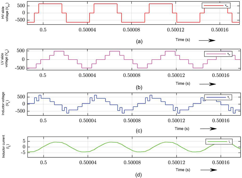
Figure 10 G2V performance evaluation of conventional MLDAB converter.
To substantiate the efficacy of the conventional FLDAB converter, the study conducts a comprehensive analysis for varying external phase shift ratios, . Encapsulation of the inductor current profile alongside their respective Total Harmonic Distortion (THD) spectra across a spectrum of values is shown in Figure 12(a–-l). The study adopts a uniform internal modulation index configuration fixed at , while systematically varying the . The resulting THD percentages are determined to be , , , , and .
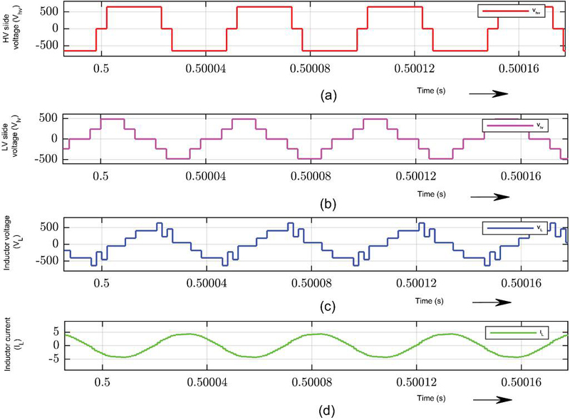
Figure 11 V2G performance evaluation of conventional MLDAB converter.
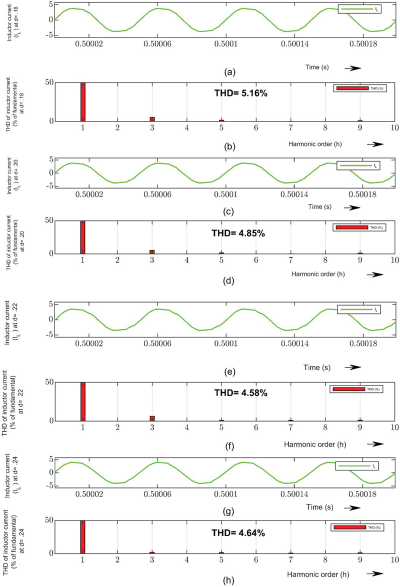
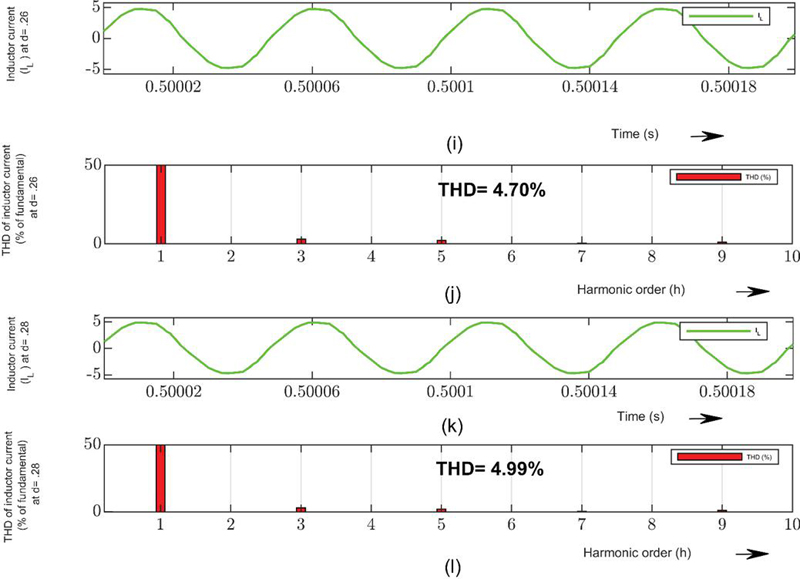
Figure 12 At different values of d performance evaluation of conventional MLDAB converter.
6.1.2 Simulation outcomes of proposed FLDAB converter using PSO algorithm based modulation
Figure 13(a–-d) comprehensively illustrates the steady-state G2V performance of the proposed MLDAB converter with PSO based modulation. Figures 13(b) and 13(a) depict the voltage waveforms at the LV and HV sides respectively, showcasing the voltage profiles generated by the modulation scheme. The inductor voltage is a result of the difference between voltages as presented in Figure 13(c). The behaviour of the inductor current as elaborated in Figure 13(d), shows a characteristic rise when the voltage across the inductor is positive and a decline during negative voltage intervals. This ensures a flow of current from the grid to the vehicle (G2V) of the MLDAB converter.
Figure 14(a–d) illustrates the V2G operational characteristics. Figures 14(b) and 14(a) present the voltage waveforms at the LV and HV sides respectively, highlighting the distinct voltage patterns achieved through the modulation scheme. The result of the voltage difference results in inductor voltage as in Figure 14(c). The behaviour of the inductor current as elaborated in Figure 14(d), shows a characteristic rise when the voltage across the inductor is positive and a decline during negative voltage intervals. This controlled variation facilitates the flow of current from the vehicle to the grid (V2G) of the MLDAB converter, thereby ensuring efficient and seamless power transfer within the system.
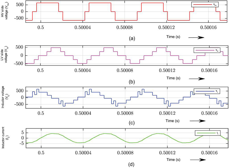
Figure 13 G2V performance evaluation of proposed MLDAB converter.
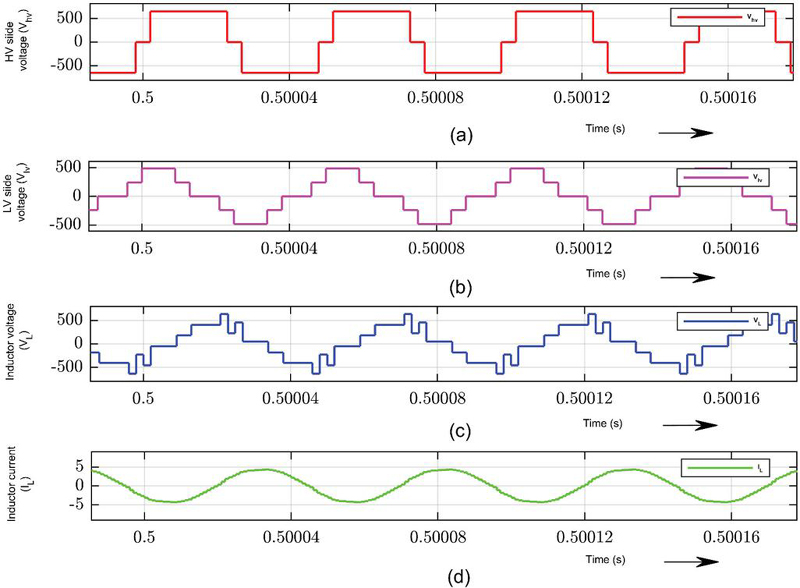
Figure 14 V2G performance evaluation of proposed MLDAB converter.
The study adopts a uniform internal modulation index configuration fixed at , while systematically varying the external phase shift ratio . The resulting THD percentages for these corresponding parameter variations are determined to be , , , , and thereby to justify the proposed modulation strategy. The operational framework considers the internal modulation index ratios assigned a value of , in conjunction with fixed at . This particular set of parameters represents the optimal configuration derived through the application of the Particle Swarm Optimization (PSO) algorithm. The objective of this optimization is to systematically minimize inherent system losses while concurrently enhancing the overall efficiency of the proposed converter, thereby achieving superior performance metrics within the defined operational limits.
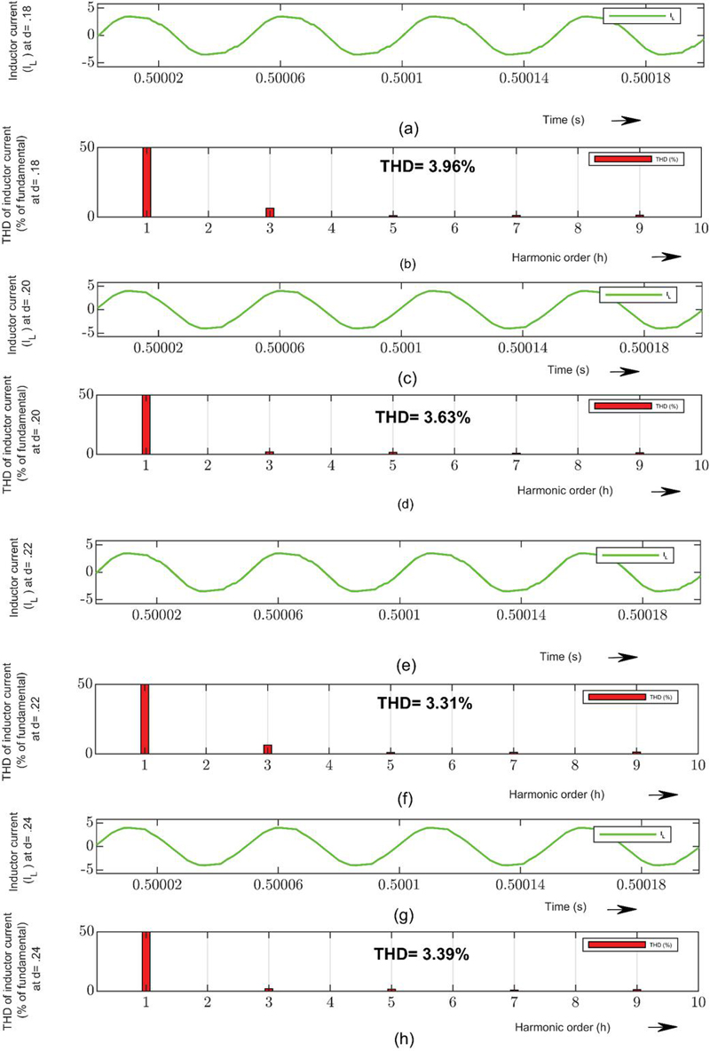
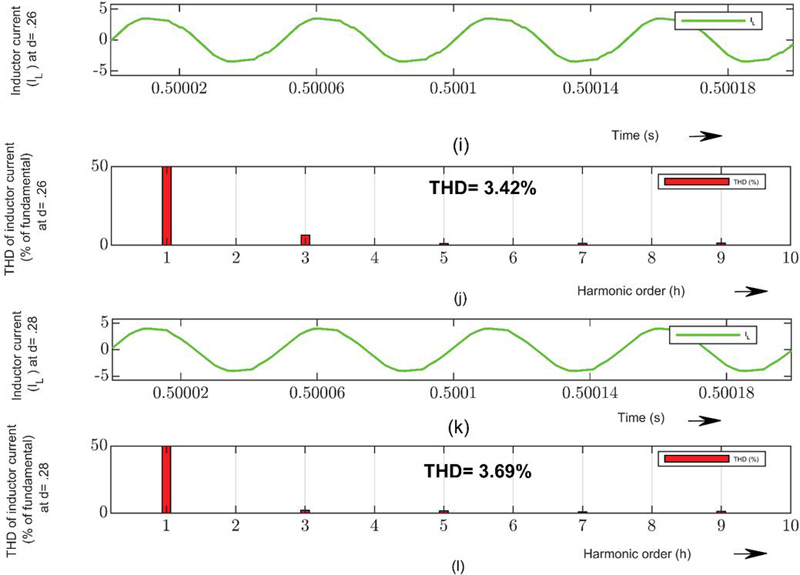
Figure 15 At different values of d performance evaluation of proposed converter.
6.2 Real Time Results
Here the validation of results using the setup as shown in Figure 16, consist of OPAL-RT (OP4510), power quality analyser, digital signal oscilloscope, and a desktop computer.
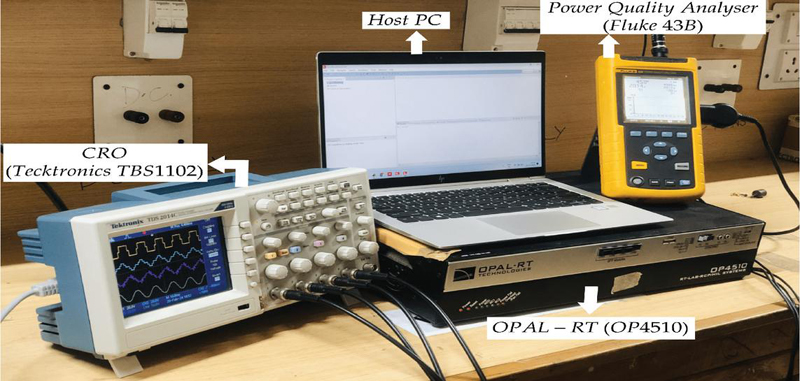
Figure 16 The setup for the validation of the results pertaining to the MLDAB converter.
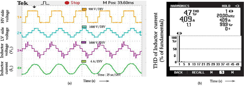
Figure 17 G2V real-time performance results.
6.2.1 Real time outcomes of conventional MLDAB converter employing QPS modulation
Figure 17(a–-b) illustrates the Real-time performance metrics of the conventional converter operating in the forward mode. The difference in voltage corresponding to the voltage across the inductor as in Figure 17(a). Additionally, the Total Harmonic Distortion (THD) of the inductor current during the G2V operation is recorded at 4.70%, as in Figure 17(b) indicating the quality of current waveform under these conditions.
Figure 18(a–-b) illustrates the Real-time performance metrics operating in the V2G mode. The voltage difference corresponding to the voltage across the inductor as in Figure 18(a). Additionally, the Total Harmonic Distortion (THD) of the inductor current during the V2G operation is recorded at 4.80%, as in Figure 18(b), indicating the quality of current waveform under these conditions.
Furthermore, this study conducts a comprehensive analysis for varying external phase shift ratios . Figure 19(a–-f) encapsulates the inductor current profiles alongside their respective THD spectra across a spectrum of values. The study adopts a uniform internal modulation index configuration fixed at , and while systematically varying the external phase shift ratio . The resulting THD percentages corresponding to these parameter variations are determined to be , , , , and respectively.
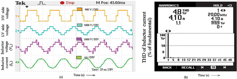
Figure 18 V2G real-time performance results.
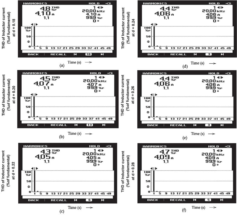
Figure 19 At different values of d, real time results related to harmonic analysis of inductor current.
6.2.2 Real time outcomes of proposed MLDAB converter using PSO algorithm based modulation
Figure 20(a–-b) illustrates the real-time performance metrics of the proposed FLDAB converter operating in the forward mode. The difference in voltage corresponding to the voltage across the inductor as in Figure 20(a). Additionally, the Total Harmonic Distortion (THD) of the inductor current during the G2V operation is recorded at 3.10%, as in Figure 20(b) indicating the quality of current waveform under these conditions.
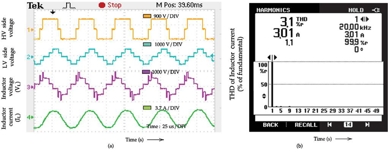
Figure 20 G2V real-time performance results of the proposed converter.
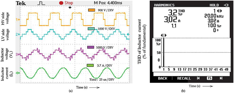
Figure 21 V2G real-time performance of the proposed converter.
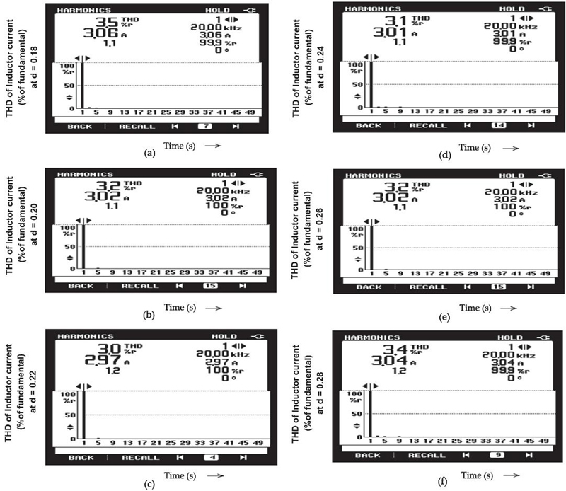
Figure 22 At different values of , real time results related to harmonic analysis of inductor current.
Figure 21 illustrates the real-time performance metrics operating in the V2G mode. The voltage difference corresponding to the voltage across the inductor as in Figure 21(a). Additionally, the Total Harmonic Distortion (THD) of the inductor current during the V2G operation is recorded at 3.20%, as in Figure 21(b), indicating the quality of current waveform under these conditions.
Furthermore, this study conducts a comprehensive analysis for varying external phase shift ratios . Figure 22(a–-f) encapsulates the inductor current profiles alongside their respective THD spectra across a spectrum of values. The study adopts a uniform internal modulation index configuration fixed at , and while systematically varying the as , , , , and . The resulting THD percentages corresponding to these parameter variations are determined to be as %, %, %, %, % and % respectively.
The analysis of the FFT plots clearly demonstrates reduction in the inductor current THD, thereby mitigating the associated heating effects. Furthermore, Figure 23 presents a comparative analysis of the THD of current across different values of . The results unequivocally illustrate lower THD in comparison to the conventional MLDAB converter, thereby indicating a superior harmonic performance and enhanced operational efficiency.
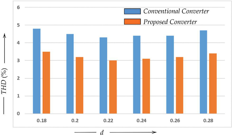
Figure 23 THD (%) plot assessment for different d values.
7 Performance Comparison
| Parameters | Voltage Level | Degrees of Freedom (DOF) | No. of (Switches + Diodes) | THD (%) | Efficiency (%) |
| SPS based DAB Converter [26] | 1 | 2 | 8 | 17.54 | 88.78 |
| EPS based DAB Converter[26] | 2 | 3 | 8 | 16.58 | 91.08 |
| DPS based DAB Converter [26] | 2 | 3 | 8 | 7.60 | 91.20 |
| TPS based DAB Converter [26] | 3 | 3 | 8 | 5.28 | 91.28 |
| QPS based MLDAB Converter[27] | 5 | 5 | 9 + 4 | 4.30 | 95.50 |
| Proposed MLDAB Converter | 5 | 5 | 10 | 3.00 | 98.00 |
This study carries out a comparative analysis to assess the performance enhancements of the proposed MLDAB converter harnessing PSO based phase shift modulation. The findings indicate that harmonics is lower than that of the conventional MLDAB converter as depicted in Figure 23. Furthermore, the proposed converter achieves improved efficiency, as illustrated in Table 6 for a power rating of 1kW and for different power ratings as shown in Figure 24, demonstrating its superior performance.
The proposed MLDAB converter topology, leveraging a PSO-based modulation scheme, achieves a five-level output with a minimized component count, thereby optimizing the overall efficiency. In contrast to the conventional converter, which necessitates four diodes for operation, the proposed MLDAB converter employs a single strategically placed active switch, thereby obviating the need for multiple components. This reconfiguration not only includes a considerable reduction in component count but also a substantial decrement in the overall system cost, thus reinforcing its economic viability without compromising performance metrics.
Furthermore, an examination of the conventional topology reveals that the current conduction trajectory involves an active switch in series with two diodes, as delineated in Figures 2 and 3. Conversely, the suggested topology redefines the operational conduction path, wherein the same functionality is realized exclusively by an active switch and a single diode, as illustrated in Figures 7 and 8. This redistribution of switching elements significantly alleviates the inherent circuital complexity while simultaneously augmenting the system’s operational resilience.
Moreover, the implications of harmonic distortions in the HFL inductor current manifest in increased root-mean-square (RMS) current, which in turn results in a pronounced escalation in harmonics, results in excessive thermal stress within the system components, thereby imposing severe constraints on the overall system efficiency and long-term operational integrity. However, the integration of the PSO-driven modulation scheme within the proposed topology yield a profound attenuation of harmonic distortions, facilitating a near-sinusoidal inductor current profile. This sinusoidal current waveform significantly mitigates thermal accumulation within the HFT, thereby prolonging its operational lifespan while concurrently diminishing maintenance and failure probabilities.
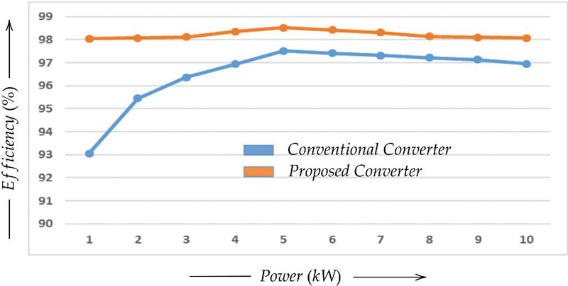
Figure 24 Efficiency assessment for different power ratings.
In culmination, the symbiotic interplay of reduced economic burden, enhanced circuital simplicity, and superior reliability to achieve a high-efficiency, low-harmonic operation within a optimized framework substantiates its viability as an indispensable alternative to conventional power conversion topologies.
8 Conclusion
This paper presents a novel five-level dual active bridge (FLDAB) converter topology using PSO based modulation technique. The proposed topology designed to reduce inductor current harmonics as well as reduced component count, thereby decreasing losses and improving the efficiency, resulting in the overall enhanced performance. This study develops and simulates the suggested MLDAB converter with PSO algorithm-based modulation within the MATLAB/Simulink environment. The analysis reveals that the proposed MLDAB converter produces a nearly sinusoidal HFL current waveform. Furthermore, the results have been compared with those obtained from the conventional converter and it shows that the proposed MLDAB converter achieves lower inductor current harmonics across a broad range of operating conditions, as well as the increased efficiency is achieved. The OPAL-RT emulator results further validate these findings.
Biographies

Khurshid Ul Haq received his Bachelor’s degree in Electrical Engineering from Jammu University and his Master’s degree in Power Electronics and Drives from Kurukshetra University, Kurukshetra. He is currently pursuing a Ph.D. in Power Electronics and Electric Drives at the Department of Electrical Engineering, National Institute of Technology (NIT), Srinagar. His research interests include power electronics, DC–DC Converters, AC–DC Converters, Improved Power Quality Converters, and Electric Vehicle Battery Chargers.

Farhad Ilahi Bakhsh (Senior Member, IEEE) received B. Tech degree in Electrical Engineering and M. Tech. degree in Power Systems & Drives from Aligarh Muslim University (AMU), Aligarh, India in 2010 and 2012, respectively. Then he pursued Ph.D. from Indian Institute of Technology Roorkee, India in 2017. During his Ph.D. he developed a new method for grid integration for wind energy generation system which has been recognized worldwide. Currently he is serving as Assistant Professor in Department of Electrical Engineering, National Institute of Technology Srinagar, Jammu & Kashmir, India. His research area of interests includes Performance Analysis and new applications of Variable Frequency Transformer, Application of Power Electronics & Drives in Renewable Energy Systems (Solar & Wind), Multilevel Converters, Multilevel DC-DC DAB Converters, Alternate Energy Vehicles (Electric/ Hybrid) and Multi-phase Drives.

Obbu Chandra Sekhar received his B. Tech degree in Electrical & Electronics Engineering from JNTUH, India in 2005 and M. Tech with power Electronics and Electrical Drives from Vignan’s Engineering College, Vadlamudi, India in 2008. He obtained his Ph. D. from J.N.T.U College of Engineering, Hyderabad in 2014. Currently he is serving as a Professor in Department of Electrical Engineering, National Institute of Technology Delhi, India. His Research interests are Power Electronics and Electric Drives.
Distributed Generation & Alternative Energy Journal, Vol. 40_2, 361–400.
doi: 10.13052/dgaej2156-3306.4027
© 2025 River Publishers