Parameter Extraction Method of Meta Equivalent Circuit Based on VIE-MoM-PEEC Algorithm
Xin Wu* and Haiyan Liu
School of Electronic Engineering, Zhengzhou Railway Vocational & Technical College, Zhengzhou, 410000 China
E-mail: wuxwxin@outlook.com
*Corresponding Author
Received 09 July 2025; Accepted 13 August 2025
Abstract
Equivalent circuit parameter extraction can reflect the electrical characteristics of actual components or systems, but there are problems such as parameter correlation at different scales, balance between calculation accuracy and efficiency in the process of circuit extraction. A new method for extracting circuit parameters is proposed. This method combines the volume integral equation algorithm and the method of moments to handle both dielectric and conductor regions. Classical surface-based and edge-based basis functions are used to discretize the conductor structure, ensuring numerical stability and convergence. In addition, multi-branch basis functions are introduced for port excitation modeling, which improves the simulation accuracy for complex port geometries. The experimental results show that the voltage pressure test results and time differences are 0.01, 0.02, 0.02, 0.03 in 697 to 1650000 grids, with the maximum being 0.03 and the minimum being 0.01. The small difference between the voltage pressure test calculation results and the reference values proves that the partial element equivalent circuit method of the volume integral equation algorithm and the moment algorithm has good computational accuracy and precision in large-scale grid computing. The above results indicate that the method proposed by the research institute has good accuracy and multi-layer interconnectivity in extracting circuit parameters, providing theoretical support for the subsequent development of circuit parameter extraction.
Keywords: Method of moments, volume integral equation algorithm, partial element equivalent circuit, circuit parameter extraction, grid subdivision.
1 Introduction
As a bridge between electromagnetic modeling and circuit simulation, equivalent circuit parameter extraction technology plays a key role in high-speed interconnection, electromagnetic compatibility (EMC) design and multi-physics field simulation. Among them, Meta Equivalent Circuit (MEC), as an abstract modeling method that integrates electromagnetic field theory, material properties, and circuit topology, can effectively describe the macroscopic electrical behavior of complex electromagnetic systems [1]. By accurately extracting parameters such as resistance, inductance and capacitance in MEC, circuit modeling of complex structures can be achieved, thereby supporting system-level functional simulation, fault diagnosis and optimization design [2]. However, in high-frequency, large-scale, or heterogeneous material scenarios, existing parameter extraction methods face a series of challenges, such as lengthy modeling processes, difficulty in balancing accuracy and efficiency, and inability to uniformly handle dielectric and conductor areas.
In this context, Shi J et al. proposed a control parameter extraction model for reconfigurable bandpass filters to address the problem of rapid reconstruction of the center frequency and bandwidth of circuits. The implementation results showed that the root mean square errors of the center frequency and bandwidth in the model were 0.0098 and 0.0129, respectively, which could effectively extract parameters [3]. Wei P et al. proposed a parameter extraction method for silicon-based small signal equivalent circuit models to address the issue of low efficiency in extracting circuit model parameters. The experimental results showed that this method operated at a frequency of up to 40 GHz on complex small signal models, improving the efficiency of parameter extraction [4]. Bosman D et al. proposed a two-dimensional differential surface admittance operator and electric field integral equation (EFIE) method to address issues related to the evolution of operating frequency and integrated density of magnetic materials in state-of-the-art interconnect designs. The experimental results showed that this method could extract the relevant unit length resistance and inductance parameters of the modeled structure, proving the correctness and universality of the method [5].
Partial Element Equivalent Circuit (PEEC) is a hybrid modeling method that combines electromagnetic field theory and circuit analysis to address parasitic effects, coupling effects, and frequency characteristics of complex electromagnetic structures. Helali H et al. proposed a new method that combined Method of Moments (MoM) and generalized equivalent circuit method to address the issue of the impact of quantity on frequency range in different miniaturized communication systems. The experimental results showed that the research method could effectively detect different frequencies at different distances, with the best bandwidth reaching 526 MHz [6]. Abdi M and Aguili T proposed a method that combined the MoM with generalized equivalent circuits to address the problem of complex structures that exceed the capabilities of a single method or standard software using mixed numerical methods. The experimental results demonstrated the multi-functionality and effectiveness of the MoM and the generalized equivalent circuit method in complex scenarios, reaffirming their value in electromagnetic modeling [7]. Hetita I et al. proposed a method based on time-domain finite difference technique and partial component equivalent circuit to address the issues of battery degradation, complete damage, service interruption, and increased maintenance costs that may occur when photovoltaic arrays are struck by lightning. The experimental results showed that the average absolute errors of the time-domain finite difference technique and the PEEC method were 5% and 11%, respectively, confirming the accuracy of the time-domain finite difference technique simulation model [8]. Mehri A et al. proposed a new accurate and effective electromagnetic transient model for grounding systems to address the vulnerability of photovoltaic systems to lightning strikes. The experimental results indicated that the frequency dependence of photovoltaic factors and soil had a significant impact on the overvoltage of photovoltaic systems. The proposed model improved accuracy by covering the entire frequency range of interest [9]. Ye W et al. proposed a new efficient full wave component equivalent circuit method for the analysis of lightning transient with uniform and damaged air, using a full space thin line structure. A three-dimensional cubic interpolation scheme was adopted to accelerate the calculation of the Sommerfeld integral. The experimental results indicated that the research method had good continuity and symmetry, which was crucial for the success of interpolation [10].
In summary, the current mainstream equivalent circuit parameter extraction methods include MoM, the volume integral equation (VIE) method for heterogeneous media analysis, and PEEC, which enables electromagnetic-circuit mapping. Although these methods have achieved some success in specific areas, they still have significant limitations. MoM has difficulty modeling the polarization response within the dielectric, while VIE is computationally expensive when dealing with large-scale structures and lacks an efficient coupling mechanism. While PEEC can achieve parametric circuit modeling, it has stringent requirements for meshing and physical boundary conditions, making it difficult to independently adapt to complex structures and multi-physics coupling scenarios. To this end, this paper proposes a hybrid VIE-MoM-PEEC algorithm for equivalent circuit parameter extraction, aiming to improve parameter extraction efficiency by integrating the advantages of all three. By unifying the meshing and data structure, the modeling of bulk current and capacitance effects in the dielectric region is synergistically coupled with the modeling of surface current, resistance, and inductance in the conductor region. PEEC is then used as an intermediary to achieve an efficient mapping from electromagnetic field parameters to circuit topology.
The research innovations are reflected in the following aspects: First, a deep integration of VIE, MoM, and PEEC is proposed to construct a unified parameter extraction and computational framework, overcoming the multiple solvers and weakly coupled interfaces required by traditional electric field-circuit synergy methods. Second, the classical Rao-Wilton-Glisson (RWG) and Schaubert-Wilton-Glisson (SWG) basis functions are used to efficiently discretize the conductor structure, ensuring numerical stability. Multi-branch basis functions are also introduced in port modeling to adapt to complex geometric topologies and enhance port excitation accuracy.
The study proposes a hybrid VIE-MoM-PEEC modeling and parameter extraction method, enabling the coordinated solution of polarization currents in the dielectric region and induced currents in the conductor region on a unified grid. By constructing an equivalent circuit mapping model based on electromagnetic solution results, combining a multi-branch port modeling strategy with a PEEC equivalent device network, the modeling accuracy and adaptability of highly complex structures are improved. Furthermore, the algorithm framework enhances grid reuse and data flow consistency mechanisms, effectively reducing the computational complexity of large-scale high-frequency structures and possessing excellent potential for parallelization and engineering deployment.
2 Methods and Materials
2.1 Construction of Equivalent Circuit Model
To extract the equivalent circuit parameters of the element, an equivalent circuit model is first established. Simulation Program with Integrated Circuit Emphasis (SPICE) is a computer language and software tool used for electronic circuit simulation, mainly used for simulating and analyzing the behavior of electronic circuits, including linear, nonlinear, time-domain, and frequency-domain characteristics. The main feature of SPICE is the use of text-based netlists to describe circuit structures, and it supports various electronic components such as resistors, capacitors, inductors, diodes, and transistors, with strong simulation capabilities. The study introduces SPICE to establish an equivalent circuit model. In SPICE circuit language, each current can control the current source, as shown in Equation (1).
| (1) |
In Equation (1), represents the positive node of the current source, represents the negative node of the current source, and is the voltage source that controls the flow of current. In SPICE, current controlled current source (CCCS) is a controlled component commonly used to construct circuits such as current amplifiers and ideal transformer models. Its proportional coefficient can be positive or negative, representing the output current and control current in the same or opposite direction, respectively. The voltage source is connected in series with the device to detect and control the current. The series connection process is shown in Figure 1.
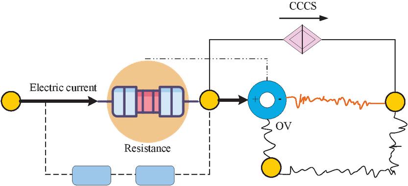
Figure 1 SPICE current series diagram.
As shown in Figure 1, when CCCS is set in SPICE, the detection of its control current must rely on a zero value independent voltage source to extract the current flowing through the target node as the control signal. The study inserts a 0 V independent voltage source into the target branch of the original circuit (such as the branch where resistors, transistors, and other devices are located) to monitor and control the current. In the circuit model, the reasonable selection of PEEC matrix equation port excitation method directly affects the accuracy, computational efficiency, and physical correctness of the results. Therefore, the study introduces port excitation method. The port excitation methodis a technique used to apply input signals or excitation sources. It applies voltage or current signals to specific ports (input/output nodes) of a circuit to simulate actual working conditions, excite the dynamic characteristics of the circuit (such as frequency response and transient behavior), and verify design functionality. In order to achieve precise solution of the circuit, multiple current sources and voltage sources are studied and set up. The schematic diagram of its port excitation is shown in Figure 2.
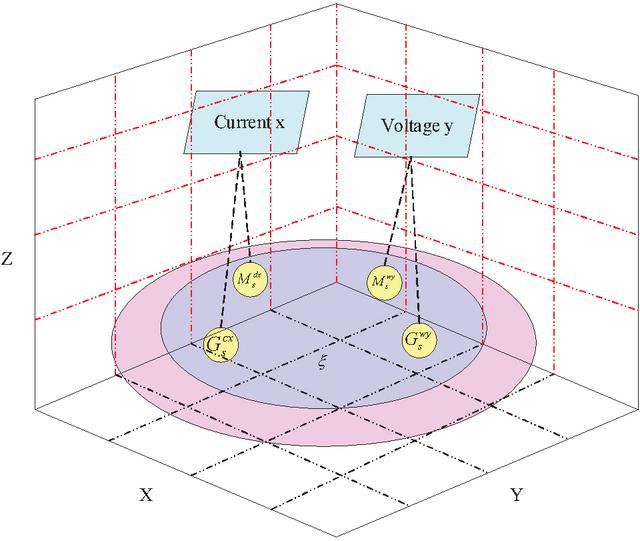
Figure 2 PEEC port excitation diagram.
As shown in Figure 2, the number of voltage and current sources in region is represented by and . ports represent the th current source and is the number of geometries on port . ports represent the th voltage source and is the number of geometries on port . The number of discrete units in region is , where represents the total number of basis functions. The port geometry is defined based on a multi-branch basis function selected by Haff. Compared to the traditional single-boundary-supported RWG/SWG basis functions, multi-branch basis functions allow for the simultaneous presence of multiple conductor boundary support points within a port region. This allows for more flexible characterization of irregular port geometries and improves the local accuracy and boundary continuity of port excitation. The expression for the multi-branch basis function is shown in Equation (2).
| (2) |
In Equation (2), represents the total number of multi-branch basis functions selected by Haff, and the above equation is extended to form an augmented matrix as shown in Equation (3).
| (3) |
In Equation (3), the zero matrix is represented by , the voltage source coefficient connected matrix is represented by , the current matrix is represented by , and the number of voltage sources is represented by . and are the voltage source and current source. The current is obtained by solving the equation, and the current vector is expressed as shown in Equation (4).
| (4) |
In Equation (4), the current of the SWG basis function with the number is represented as , and the current of the multi-branch basis function with the number is represented as . The voltage vectors of the internal and port nodes are shown in Equation (5).
| (5) |
In Equation (5), the internal potential and port potential of number are and . Based on the above results, a corresponding SPICE simulation model is constructed based on the PEEC modeling results. The extracted equivalent parameters R (resistance), L (inductance), and C (capacitance) are mapped to series resistance, mutual coupling inductance, and ground/node capacitance components in the SPICE network, respectively. All equivalent devices are connected through a topological structure to form a multi-port network. To simulate the effects of external excitation on the structure under test, CCCS is introduced as the excitation input to ensure consistency between the current source and the structural response during the simulation. Furthermore, all port node numbering and connection methods strictly follow the sequential numbering consistent with the VIE-MoM-PEEC grid to ensure the accuracy of the topological mapping.
2.2 Design of Meta Equivalent Parameter Extraction Method Based on VIE-MoM-PEEC
2.2.1 Dielectric region modeling based on VIE
After the establishment of the equivalent circuit model, the study designs the method for extracting the meta equivalent parameters of VIE-MoM-PEEC. In computational electromagnetics, there are two closely related cores. One is the VIE, which is used to analyze electromagnetic field problems in non-uniform, anisotropic, or complex media, and to solve the limitations of traditional methods (such as differential equation methods) in dealing with certain electromagnetic problems [11, 12]. The second is the Volume Equivalence Principle (VEP), which is used to transform electromagnetic field problems in complex media into equivalent free space radiation problems. In the process of calculating electromagnetics, when electromagnetic waves are incident on a medium, they will interact with the medium, exciting the polarization current and magnetization current inside the medium. These induced currents will act as secondary radiation sources to re radiate electromagnetic waves, thereby changing the total electromagnetic field distribution in space. The process of these waves interacting with matter and causing changes in the field distribution is collectively referred to as electromagnetic scattering phenomena [13, 14]. On the basis of VEP, the principle of electromagnetic scattering phenomenon of VIE is shown in Figure 3.
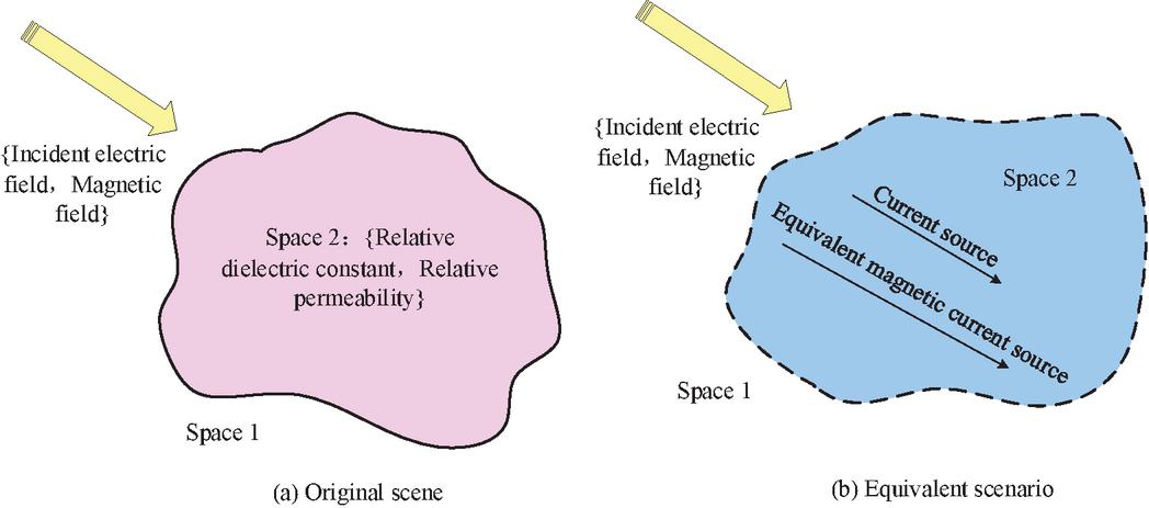
Figure 3 Schematic diagram of body equivalence principle.
From Figure 3(a), it is a volume equivalent original scene, where there is a spatial medium volume 2 on the background space 1, which contains the relative dielectric constant and relative magnetic permeability. The background space 2 also has its own relative dielectric constant and relative magnetic permeability. From Figure 3(b), it is a volume equivalent scenario, where the incident electric and magnetic fields enter the spatial medium body 2. Based on the principle of volume equivalence, the electromagnetic effect of medium body 2 can be equivalent to a volume equivalent current source and a volume equivalent magnetic current source, thereby transforming the entire region into a uniform medium space. The expression of the body equivalent current source throughout the entire process of the body equivalent principle is shown in Equation (6).
| (6) |
In Equation (6), represents the body equivalent current source, represents the relative dielectric constant, and represents the electric field intensity vector at the spatial position . The expression for the equivalent magnetic current source is shown in Equation (7).
| (7) |
In Equation (7), represents the equivalent magnetic current source, represents the relative magnetic permeability, and represents the magnetic field intensity vector at the spatial position . The total field is obtained by superimposing the incident lengths, and its equation is shown in Equation (8).
| (8) |
In Equation (8), represents the incident electric field and represents the scattered electric field. The superposition of scattered fields can obtain the total field, and the expression of the total field is shown in Equation (9).
| (9) |
In Equation (9), represents the incident magnetic field and represents the scattered magnetic field.
2.2.2 Conductor area modeling based on MoM
To solve the problems of electromagnetic scattering, radiation analysis, and high-frequency parasitic parameter extraction in open spaces, the MoM is introduced [15, 16]. MoM is a classical numerical method used in computational electromagnetics to solve integral equations. Its core idea is to discretize continuous integral equations into matrix equations and obtain approximate solutions to unknown variables through numerical solutions. By dividing the target surface into triangular and quadrilateral elements, and discretizing the three-dimensional target body using tetrahedral elements, the geometric basis for electromagnetic calculations can be constructed. The integral equation can be expressed as a linear mathematical operator, and the expression of the linear mathematical operator is shown in Equation (10).
| (10) |
In Equation (10), represents a linear operator, represents the left-hand excitation function, and represents the right-hand excitation function. The implementation process of MoM includes three core steps: first, discretizing the integral equation through basis function expansion, then establishing a linear equation system using Galerkin inner product test method, and finally solving the matrix equation obtained through direct solution or iterative algorithm. The expression of the objective function to be solved is shown in Equation (11).
| (11) |
In Equation (11), in the expansion of sparse basis function , the discretization accuracy improves with the increase of discrete basis function . In practical calculations, the implementation of the MoM requires seeking the optimal balance between numerical accuracy and computational efficiency. Through the collaborative optimization of adaptive basis function selection, matrix compression techniques, and efficient solvers, efficient calculations with controllable accuracy can be achieved. The expression for the calculation is shown in Equation (12).
| (12) |
In Equation (12), by expanding the basis function , the solving object of the original equation is transformed into the coefficient . To solve these N unknown coefficients, N independent test equations must be constructed to form a closed system. When using MoM to solve metal electromagnetic problems, before performing numerical calculations, it is necessary to first perform geometric modeling on the simulation object to accurately describe its structure and spatial relationships. The accuracy of electromagnetic numerical calculations directly depends on the precision of geometric modeling. After completing the geometric modeling, it is necessary to mesh the model, generate discrete elements, and construct appropriate basis functions on these elements to achieve numerical discretization [17]. The SWG basis function has the advantage of high computational efficiency. The introduction of SWG is studied, and its schematic diagram is shown in Figure 4.
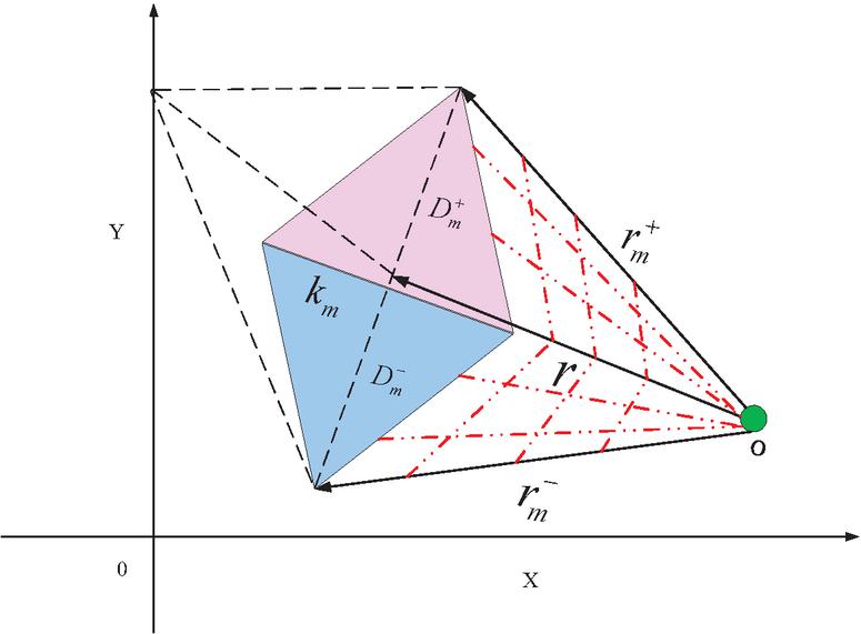
Figure 4 SWG basis function.
In Figure 4, is the length of the common side of a pair of triangles, represents the first triangle region, represents the second triangle region, represents the free vertex vector on the first triangle, represents the free vertex vector on the second triangle, and represents the free vertex. The expression for solving the basis function is shown in Equation (13).
| (13) |
In Equation (13), the RWG basis function is used to discretize the current density , and the divergence in the entire region is 0. The calculation expression is shown in Equation (14).
| (14) |
In Equation (14), the total surface charge of positive and negative units on the basis function is 0.
2.2.3 Equivalent circuit construction and mapping based on VIE-MoM-PEEC
PEEC is an analysis method that transforms electromagnetic field problems into circuit models, mainly used for EMC, signal integrity (SI), and power integrity (PI) simulations of high-frequency and interconnect structures [18, 19]. The research introduces PEEC to solve high-frequency interconnect design and electromagnetic circuit coordination problems. The PEEC model is derived based on the EFIE, which converts electromagnetic quantities into corresponding circuit parameters. By forcibly satisfying the current continuity condition, it ensures that the discretized equivalent circuit strictly conforms to the conservation characteristics of the actual electromagnetic field, thereby ensuring the correctness of the model [20]. The EFIE is derived, and its expression is shown in Equation (15).
| (15) |
In Equation (15), an equivalent circuit is established by discretizing and . To achieve efficient analysis of complex systems in multiple physical fields, a VIE-MoM-PEEC hybrid method is developed by combining VIE, MoM, and PEEC. Non-uniform media (such as insulating materials and magnetic cores) is discretized into bulk current units using the principle of bulk equivalence, and the electromagnetic response of polarized current is calculated. The surface of the conductor is discretized and the surface current is solved using the surface integral equation. The current distribution of VIE and MoM is transformed into a distributed RLCG circuit network to achieve the mapping of electromagnetic parameters to circuit parameters. The implementation process of VIE-MoM-PEEC is shown in Figure 5.
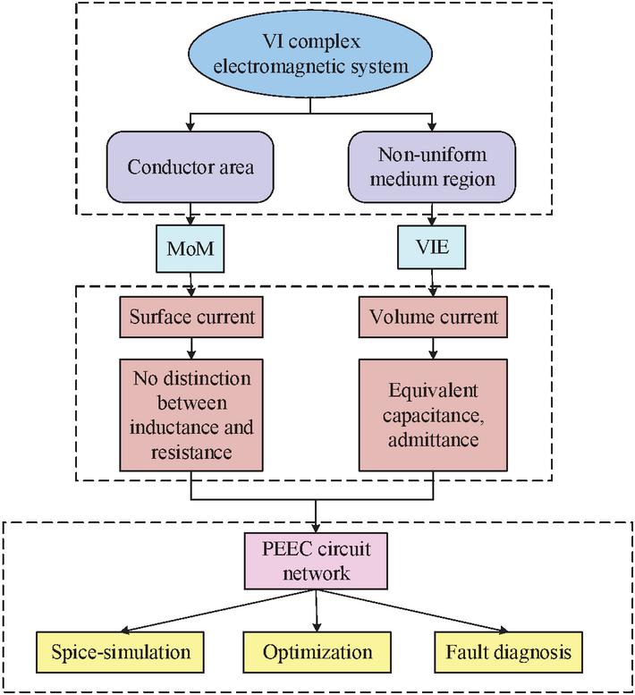
Figure 5 Implementation flowchart of VIE-MoM-PEEC.
As shown in Figure 5, the VIE-MoM-PEEC framework takes a complex electromagnetic system as input and divides it into conductor regions and inhomogeneous dielectric regions, depending on the physical domain. The conductor region is modeled using MoM to solve for the induced current on the conductor surface, thereby extracting the resistance and inductance characteristics. The dielectric region is modeled using VIE to calculate the polarized bulk current and derive the equivalent capacitance and susceptance parameters. Regarding the boundary interaction mechanism, the VIE and MoM share a shared boundary current density. At the dielectric-conductor interface, the conductor surface currents obtained by MoM are used as the excitation source term in the VIE boundary conditions. The polarized currents inverted in the VIE are then fed back to correct the equivalent impedance boundary in the MoM, thereby achieving bidirectional coupling between the electric field and current distributions in the two regions. Furthermore, to maintain modeling consistency, both the VIE and MoM use a uniformly numbered mesh, and the PEEC module implements a structural mapping of the coupled data to the circuit topology. Serving as a bridge between the electromagnetic and circuit domains, PEEC receives the equivalent physical parameters output by the VIE and MoM and constructs a unified RLC network structure. The entire process of extracting circuit parameters using partial element equivalence based on VIE-MoM-PEEC is shown in Figure 6.
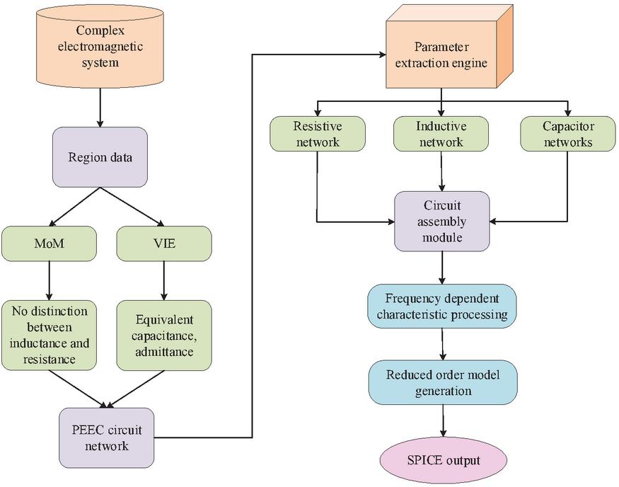
Figure 6 VIE-MoM-PEEC parameter extraction process.
From Figure 6, the entire process of extracting circuit parameters based on VIE-MoM-PEEC partial element equivalence involves inputting regional data in a complex circuit, using MoM algorithm and VIE algorithm to calculate inductance resistance and capacitance admittance respectively, and then exporting the final data and transmitting it to the PEEC circuit network. Then, the parameter extraction engine is used to obtain the circuit assembly module composed of the resistance network, inductance network, and capacitance network. The process performs frequency characteristic processing on the circuit, generates a reduced order model, and finally outputs the result by SPICE.
3 Results
3.1 VIE-MoM-PEEC Algorithm Performance Test
The VIE-MoM-PEEC algorithm achieves numerical discretization by exciting the polarization current and magnetization current inside the medium, and selecting basis functions through geometric construction. An equivalent circuit topology network was constructed using multi-branch basis functions to ensure that the discretized equivalent circuit strictly conformed to the conservation characteristics of the actual electromagnetic field, thereby ensuring the correctness of the model. As a key support for circuit parameter extraction, the main configuration of the computer environment used in the study is shown in Table 1 in terms of computer hardware.
Table 1 Test platform configuration table
| Name | Parameter |
| Processor | Intel(R)Core(TM)i5-6200u CPU@2.3GHz |
| RAM | 32GB |
| Operating system | Windows, Linux |
| Graphics card model | NVIDIA Tesla A10 24G GUP |
| GPU driver | NVIDIA Driver Version 535.104.05 |
| CUDA Version | CUDA Toolkit 12.2 |
| Memory module model | DDr5 |
As shown in Table 1, the simulation platform used in this study ran on a dual-OS (Windows and Linux) workstation equipped with an Intel(R) Core(TM) i5-6200U @ 2.3GHz processor, 32GB of RAM, and an NVIDIA Tesla A10 24GB graphics card. The core algorithms were implemented in Python 3.10 and C++, both of which support parallel computing. Graphics computing was based on the CUDA Toolkit 12.2 and NVIDIA Driver 535.104.05. Circuit solving was performed using the LTspice platform, and auxiliary modeling and verification tools included Cadence Sigrity and custom-developed modules. To verify the accuracy and applicability of the Volume Integral Equation Method of Moments (VIE-MoM), the scattering of a two-layer lossy medium cylinder was selected as an example to analyze the efficiency, memory consumption, and other aspects of the method. The simulation platform was jointly built based on CST and LTspice. All materials were assumed to be ideal conductors and the spatial medium was uniform air. The two-layer medium cylinder dual station is shown in Figure 7.
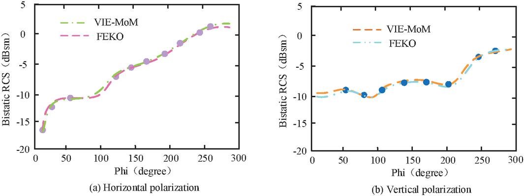
Figure 7 Two layer medium cylinder double station diagram.
According to Figure 7, the structural parameters of the cylinder were as follows: the cylinder had a height of 0.5 m, an inner-cylinder bottom radius of 0.2 m, and an outer-cylinder bottom radius of 0.3 m. The boundary conditions were set as open-domain absorbing boundaries to ensure that reflections were minimized, and the excitation duration was 10 ns for extracting the transient voltage distribution and parametric response characteristics. The relative magnetic permeability of both layers of cylinders was 1.0. SWG basis functions were formulated, and the dual-station RCS of the target was calculated separately under horizontal polarization and vertical polarization. From Figure 7(a), it was observed that the horizontal polarization values obtained from the two methods were highly consistent, with only very small errors. From Figure 7(b), the predicted vertical-plane values of the two methods were also found to be highly consistent, with small errors present. Combining Figures 7(a) and 7(b), as the grid size increased, the simulated impedance value gradually stabilized, and the error convergence range was controlled within 0.5%, showing good numerical consistency. The results indicated that the research algorithm demonstrated significantly high computational accuracy in multi-layer media calculations, thereby proving the algorithm’s accuracy. Table 2 shows the comparison of resistance and inductance values and relative errors between VIE-MoM and FEKO at different frequencies.
Table 2 shows a comparison of resistance and inductance parameters at three typical frequencies, 1 Hz, 1 kHz, and 1 MHz, and verifies the results with calculations using the commercial simulation software FEKO. As can be seen, for resistance, the relative error between the two was within 2.61%, while for inductance, the maximum relative error did not exceed 1.09%. Overall, the VIE-MoM method demonstrated high consistency and numerical stability across different frequencies, demonstrating its applicability and engineering feasibility in broadband modeling scenarios. On this basis, the effectiveness and computational accuracy of the proposed method in multiple frequency bands were further analyzed. A helical structure was selected as the parameter extraction verification target. The structure consisted of a rectangular conductor with a radius of 0.5 mm and a height of 2 mm. The connecting wires at both ends were 0.06 mm long, 0.5 mm wide, and 0.06 mm high. The entire structure was placed in a homogeneous medium, and the boundary conditions were set as perfect conductor closed boundaries to suppress external interference. During the test, ports were set at both ends of the model for excitation and response measurements. The excitation signal was swept in the frequency domain from 1 Hz to 1 GHz. The port impedance was calculated using the VIE-PEEC method and ANSYS Maxwell software. The response results and relative errors at different frequencies were compared, as shown in Figure 8.
Table 2 Comparison of calculation results of VIE-MoM and FEKO methods at different frequencies
| VIE-MoM | FEKO | Relative | VIE-MoM | FEKO | Relative | |
| Frequency | Resistance | Resistance | Resistance | Inductance | Inductance | Inductance |
| (Hz) | () | () | Error (%) | (nH) | (nH) | Error (%) |
| 1 | 1.12 | 1.15 | 2.61 | 4.25 | 4.31 | 1.39 |
| 1000 | 1.24 | 1.27 | 2.36 | 4.87 | 4.93 | 1.22 |
| 1000000 | 1.58 | 1.58 | 1.86 | 5.46 | 5.51 | 0.91 |
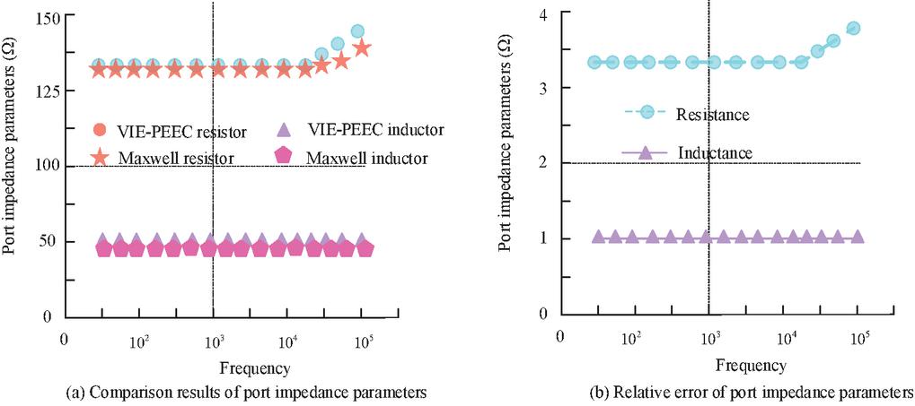
Figure 8 Comparison results and relative error chart of port impedance parameters.
From Figure 8(a), from the low-frequency range to the high-frequency range, the resistance calculated by the VIE-PEEC algorithm exhibited small fluctuations and was highly consistent with the results tested by ANSYS Maxwell software. The inductance determined by the VIE-PEEC algorithm remained relatively stable, showing no significant changes, and was also highly consistent with the results obtained from ANSYS Maxwell software tests. According to Figure 8(b), within the frequency range of 1 Hz to 1 GHz, error analysis conducted by the VIE-PEEC algorithm and ANSYS Maxwell software revealed that the average deviation of inductance calculation results was 0.1%, and the average deviation of resistance calculation results was 0.5%. It was also capable of performing large-scale systematic EMC analysis. In addition, compared with commercial simulation software such as ANSYS Maxwell, the VIE-PEEC method significantly reduced computational complexity and time cost while maintaining computational accuracy, demonstrating good performance advantages and engineering applicability. It is particularly suitable for low-frequency device parameter extraction and large-scale electromagnetic modeling tasks.
3.2 Parameter Extraction Testing of MEC
To verify the adaptability and modeling accuracy of the proposed VIE-MoM-PEEC algorithm for complex structures, a typical six-layer printed circuit board (PCB) structure was constructed for testing. This multilayer PCB structure consisted of three copper conductor layers (each 0.035 mm thick, with a conductivity of S/m) and three FR4 dielectric layers (relative permittivity , loss tangent , and thicknesses of 0.15 mm, 0.10 mm, and 0.15 mm, respectively). The middle conductor layer was equipped with signal traces with a width of 0.3 mm, a spacing of 0.5 mm, and a length of 10 mm. The upper and lower layers were power planes, connected to the middle signal layer through vias to form a closed channel. Boundary conditions included periodic boundaries in the X-Y direction and open-domain radiation boundaries on the upper and lower surfaces in the Z direction to approximate a realistic electromagnetic transmission environment. The structure was parameterized using Cadence PowerDC and imported into the VIE-MoM-PEEC framework for modeling and simulation, with a frequency sweep range of 1 Hz to 1 GHz.
Cadence PowerDC software is widely used in industry for large-scale PI analysis and DC simulation of multi-layer PCB structures. It boasts highly mature modeling capabilities and commercially recognized simulation accuracy. Its solver kernel, based on the finite volume method and fast multipole algorithm, effectively handles current distribution and voltage drop calculations under complex topologies and inhomogeneous materials. Therefore, the simulation results of VIE-MoM-PEEC were compared with those of Cadence PowerDC software. The results for multi-layer interconnects are shown in Figure 9.
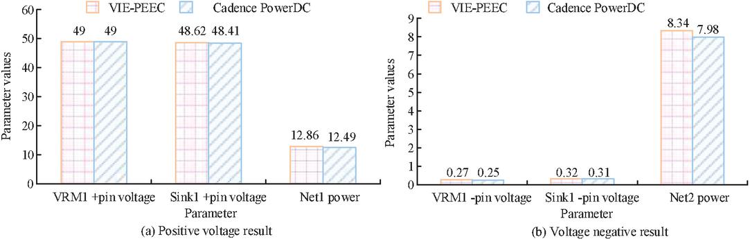
Figure 9 Comparison chart of multi-layer interconnection results.
From Figure 9(a), in the VRM1+pin voltage, both the voltage values calculated by VIE-MoM-PEEC and Cadence PowerDC were 49V, and the error between the two was 0. At the positive voltage Sink1+pin voltage of the current source, the value obtained from VIE-MoM-PEEC was 48.62, while that from Cadence PowerDC was 48.41, resulting in an error of 0.21 between the two. The Net1 power error of the circuit was approximately 0.3. As shown in Figure 9 (b), at the Sink1 pin voltage of the current source’s negative electrode, the value from VIE-MoM-PEEC was 0.32 and that from Cadence PowerDC was 0.31, with an error of 0.02 between them. In the VRM1 pin voltage, the voltage calculated by VIE-MoM-PEEC was 0.27 V and that by Cadence PowerDC was 0.25 V, with an error of 0.02 between the two. The Net2 power error was around 0.3. The comparison error between the simulation results of VIE-MoM-PEEC and Cadence PowerDC was within the range of 0.5, which was a very small error. This verified the capability of the VIE-MoM-PEEC algorithm to accurately calculate multi-layer complex interconnect structures. PEEC conducted a simple two-wire model with current and voltage sources under DC conditions, using a 1*1*10 mm two-wire model to calculate the voltage distribution characteristics, transmission power, and resistance value of a single wire along the line. The program was subjected to stress testing, and the comparison of calculation results and time is shown in Figure 10.
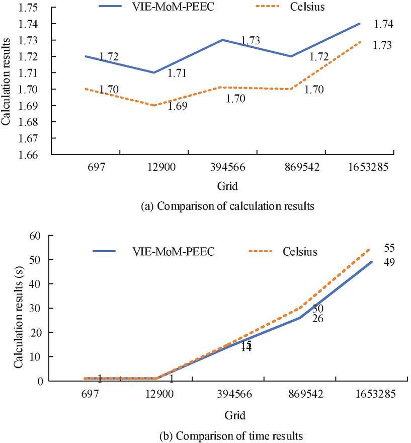
Figure 10 Comparison chart of calculation results and time results.
According to Figure 10(a), among the grid counts ranging from 697 to 1,650,000, there was an error of 0.02 at 697 grids, 0.02 at 12,900 grids, 0.03 at 394,566 grids, 0.02 at 869,542 grids, and 0.01 at 1,653,285 grids. The gap between the calculated results and the reference values was progressively narrowing, indicating that VIE-MoM-PEEC exhibited good computational performance during stress testing with large-scale grids. As shown in Figure 10(b), the computation time of VIE-MoM-PEEC was faster than that of Cadence PowerDC at grid counts of 394,566, 869,542, and 1,653,285. This demonstrated that the study could achieve a more efficient computation speed. Spiral inductors are commonly used passive components in RF integrated circuits and microwave circuits. The extraction of their impedance parameters was crucial for circuit design and performance optimization. In the study of the inductance model of copper conductors ( S/m), the skin effect was investigated when the frequency changed from 1Hz to 1MHz. The frequency-variation characteristics of AC resistance and inductance parameters were quantitatively analyzed. Using tetrahedral mesh partitioning, 800 tetrahedral elements were generated and tested using VIE-MoM-PEEC and ANSYS Q3D software. The comparison results of resistance and inductance simulations are shown in Table 3.
Table 3 Comparison results table of resistance and inductance
| Index | Frequency | VIE-MoM-PEEC | Q3D |
| Comparison of resistance calculation | IE5 | 1.21E | 1.19E |
| IE6 | 1.21E | 1.19E | |
| IE7 | 1.21E | 1.19E | |
| IE8 | 1.21E | 1.19E | |
| IE9 | 1.8E | 1.1E | |
| Comparison of inductance calculation | IE5 | 3.99 | 3.9 |
| IE6 | 3.99 | 3.9 | |
| IE7 | 3.99 | 3.9 | |
| IE8 | 3.99 | 3.9 | |
| IE9 | 3.5 | 3.3 |
According to Table 3, the resistance results of VIE-MoM-PEECwere 1.21E at frequencies IE5–IE8, and 1.21E at frequency IE9. The resistance result of Q3D in frequencies IE5–IE8 was 1.19E, and the resistance between 1Hz-100kHz had a calculation error of 0.02 . At frequencies IE5–IE8, the inductance results of VIE-MoM-PEECwere all 3.99. The inductance result of Q3D in frequencies IE5–IE8 was 3.9, and the calculation error of inductance was about 0.09 nH. As the frequency gradually increased from 1Hz to 1GHz, the overall resistance value remained relatively stable until a significant increase occurred at 1 GHz. This phenomenon was mainly attributed to the enhanced high-frequency skin effect. When the frequency increased, the current in the conductor tended to concentrate on the surface, resulting in a decrease in the effective conductive cross-sectional area, which in turn caused an increase in resistance. In addition, at extremely high frequencies, higher mesh density and dielectric resolution were required. If the mesh division failed to fully capture the changes in the current distribution boundary, a certain degree of numerical instability or error amplification may be caused. In contrast, the VIE-MoM-PEEC proposed in the study had higher accuracy in impedance parameter extraction.
3.3 Verification of Multi-physics Coupling Performance
To further demonstrate the modeling capabilities and resource efficiency of the VIE-MoM-PEEC method in electrothermal coupling scenarios, a typical multilayer copper conductor structure was selected as the simulation object. This structure consists of three parallel layers of copper strips, each measuring 10 mm 1 mm 0.1 mm. The layers were separated by polyimide (dielectric constant , thermal conductivity W/mK) insulation, with a spacing of 0.2 mm between the layers. The conductor material was high-conductivity copper (electrical conductivity S/m, thermal conductivity W/mK). To introduce electrothermal coupling effects, a constant excitation current A was applied to the port at a frequency of MHz, accounting for Joule heating due to AC conduction losses. During the simulation, the electromagnetic field and steady-state heat conduction equations were solved, with boundary conditions including electrical and thermal boundaries and coupling mechanisms. Additionally, the proposed method was compared with ANSYS Maxwell and COMSOL Multiphysics, and the specific indicators are shown in Table 4.
Table 4 Multi-physics simulation performance comparison
| Maximum | Resistance | Inductance | Simulation | CPU | Memory | |
| Temperature | Change | Fitting | Run | Usage | Usage | |
| Method | Rise (C) | Rate (%) | Error | Time (s) | (%) | (GB) |
| VIE-MoM-PEEC | 52.37 | 3.41 | 0.12 | 16.58 | 38.75 | 4.56 |
| ANSYS Maxwell | 59.84 | 5.67 | 0.23 | 38.14 | 62.31 | 7.23 |
| COMSOL Multiphysics | 55.42 | 4.91 | 0.19 | 33.76 | 55.17 | 6.35 |
As shown in Table 4, the VIE-MoM-PEEC method predicted a maximum temperature rise of 52.37C in temperature rise simulation, significantly lower than ANSYS Maxwell and COMSOL. Regarding the resistance change rate, the VIE-MoM-PEEC prediction was 3.41%, a reduction of 39.8% and 30.5% compared to Maxwell and COMSOL, respectively. Regarding the inductance fitting error, the VIE-MoM-PEEC method reduced the error by 47.8% and 36.8% compared to Maxwell and COMSOL, respectively. Furthermore, VIE-MoM-PEEC performed well in simulation runtime, CPU utilization, and memory consumption. Its runtime of 16.58 seconds was only 43.5% of Maxwell and 49.1% of COMSOL, resulting in an average resource overhead reduction of over 40%. This demonstrated the efficiency and stability advantages of the proposed method in complex coupling scenarios.
4 Discussion
The proposed VIE-MoM-PEEC hybrid algorithm demonstrated significant advantages in electromagnetic parameter extraction, equivalent circuit mapping, and multiphysics modeling. Compared to traditional methods, this method not only achieved a unified solution for dielectric polarization currents and conductor induced currents, but also significantly improved numerical accuracy and simulation efficiency through a shared mesh structure and integrated data flow. In terms of applicable scenarios, the VIE-MoM-PEEC method was advantageous in multi-layer interconnect structures, low-frequency device modeling, and electro-thermal coupling environments. Comparative multiphysics simulation experiments showed that VIE-MoM-PEEC outperformed ANSYS Maxwell and COMSOL Multiphysics in terms of maximum temperature rise error, resistance change rate, and inductance fitting error, reducing each by over 40% while also reducing CPU usage and simulation time.
However, the method’s applicability in high-frequency scenarios remained limited. The PEEC method inherently required high mesh density for extremely high-frequency fields, which increased simulation complexity. Therefore, further optimization of the method’s stability and efficiency is needed for high-frequency modeling above the gigahertz level. In addition, its adaptability to multi-physics coupling problems with strong nonlinear material response or complex boundary conditions has not yet been fully verified, and further expansion is required in combination with nonlinear solution modules.
In terms of scalability, the grid reuse mechanism and unified data structure proposed in this paper provide a solid foundation for the parallel implementation and engineering implementation of the method. Compared with the traditional VIE method in reference [11] that requires independent grids and repeated calculations, the proposed method reduced the calculation time by about 60% under similar modeling accuracy through a structural collaborative processing mechanism. Compared with the use of MoM alone to solve metal conductors in reference [16], this method showed better stability and fitting accuracy when processing dielectric wrapped structures. It is worth noting that the trade-off between accuracy and calculation time is still the core issue in the design of this type of hybrid algorithm. The comparison results of the VIE-MoM method with FEKO at multiple frequency points showed that the resistance and inductance fitting errors were both less than 0.3%, and the simulation time was shortened by about 43.2%, reflecting a high engineering practical value. The VIE-MoM-PEEC method is an electromagnetic modeling framework that combines versatility, accuracy, and resource efficiency. It is suitable for complex interconnect structures, low-frequency devices, and electro-thermal coupling scenarios.
5 Conclusion
To address the challenges of modeling and analyzing electromagnetic systems in large-scale, low-frequency, and multi-physics coupled scenarios, this paper proposed a unified modeling and parameter extraction method based on VIE-MoM-PEEC. By collaboratively solving the polarization currents in the dielectric region and the induced currents in the conductor region on a unified mesh, high-precision RLC parameter extraction was achieved, demonstrating excellent computational accuracy, operational efficiency, and resource adaptability. Comparative experiments with commercial software such as ANSYS Maxwell and COMSOL validated the effectiveness and engineering feasibility of the proposed method for electromagnetic-thermal coupled analysis.
Nevertheless, this research still has certain limitations: the algorithm computational complexity increased significantly in high-frequency or ultra-large model simulations, placing high demands on hardware resources. Furthermore, automatic topology identification for complex geometries still relied on manual intervention, and the mesh generation and boundary setting processes were not yet fully automated. Furthermore, the currently supported multi-physics coupled scenarios were primarily linear electro-thermal analysis, not yet covering nonlinear or time-varying characteristics.
Future research will concentrate on several key areas. Firstly, GPU acceleration will be introduced to enhance the simulation efficiency of large-scale models. Secondly, automatic topology recognition and mesh conversion modules will be developed for complex structures, aiming to reduce the complexity of user operations. Lastly, exploration will be made into integrating with chip-package-board co-simulation tools to meet the modeling requirements of next-generation 3D packaging and high-density interconnect circuits.
Fundings
The research is supported by Henan Province Science and Technology Research Program Project “Research on Data Acquisition Interaction and Digital Instrument Cloud Implementation Technology Based on Embedded Measurement” (No. 222102320215); Henan Province Education Science Planning Project “Research on the Training Mode of On site Engineers in the Integrated Circuit Technology Major of Higher Vocational Education under the Background of “Chinese Chip” in the New Era” (No. 2024YB0529).
References
[1] Romano D, Kovacevic-Badstuebner I, Antonini G. Anisotropic and optimized FFT-based iterative electromagnetic solver for the PEEC method. IEEE Transactions on Microwave Theory and Techniques, 2023, 72(5): 2927–2937.
[2] Huang C, Wei E I. A Parallel Block Preconditioner-Based VIE-FFT Algorithm for Modeling the Electromagnetic Response From Nanostructures. IEEE Transactions on Antennas and Propagation, 2023, 72(1): 1051–1056.
[3] Shi J, Dong J, Zhenyu WangBin, LiuTao. YangYong WangSheng WangJihong Shen. Control Parameter Extraction Model for Reconfigurable Bandpass Filter Based on Bayesian Optimized Multiple-Output XGBoost. IEEE Microwave and wireless technology letters, 2024, 34(3): 263–266.
[4] Wei P, Deng J, Zhang W. Hybrid small-signal model parameter extraction for GaN HEMT-on-Si Substrates based on theSPF method. Journal of Computational Electronics, 2024, 23(3): 516–524.
[5] Bosman D, Huynen M, De Zutter D. Analysis and Application of a Surface Admittance Operator for Combined Magnetic and Dielectric Contrast in Emerging Interconnect Topologies. IEEE Transactions on Microwave Theory and Techniques, 2023, 71(7): 2794–2806.
[6] Helali H, Aidi M, Aguili T. Frequency reconfigurable antenna array modelling based on MoM-GEC method for RFID, WiMax and WLAN applications. Analog Integrated Circuits and Signal Processing, 2024, 118(3): 553–566.
[7] Abdi M, Aguili T. Unveiling the diverse applications and problem-solving capabilities of the MOM-GEC hybrid approach: a comprehensive systematic review. Journal of Computational Electronics, 2024, 23(4): 791–818.
[8] Hetita I, Mansour D E A, Han Y. Evaluating transient behaviour of large-scale photovoltaic systems during lightning events using enhanced finite difference time domain method with variable cell size approach. High Voltage, 2024, 9(3): 636–647.
[9] Mehri A, Ghanizadeh R, Beiraghi M. Analysis of Electromagnetic Transient Overvoltages of PV Systems Considering Frequency Dependence of Grounding System. Journal of Solar Energy Research, 2023, 8(3): 1587–1598.
[10] Ye W, Liu W, Xiang N. A full-wave PEEC model for thin-wire structure in the air and homogeneous lossy ground. IEEE Transactions on Electromagnetic Compatibility, 2023, 65(2): 518–527.
[11] Giannakopoulos I I, Guryev G D, Jose E. C. SerrallésJan PakaBei ZhangLuca DanielJacob K. WhiteChristopher M. CollinsRiccardo Lattanzi. A Hybrid Volume-Surface Integral Equation Method for Rapid Electromagnetic Simulations in MRI. IEEE Transactions on Biomedical Engineering, 2023, 70(1): 105–114.
[12] Lapich A O. Method of Volume Singular Equations for Solving a Nonlinear Problem of Diffraction in a Semi-Infinite Rectangular Waveguide. Lobachevskii journal of mathematics, 2023, 44(9): 4028–4033.
[13] Xiaojia D U, Liao Z, Zhe L I. Influence of ship motion on radar cross section probability density under grazing incidence. Chinese Journal of Ship Research, 2023, 18(2): 211–217.
[14] Liu R, Wu K. Near-Field Technologies for Multifunction Wireless Connectivity: Recent principles and applications. Antennas & Propagation Magazine, IEEE, 2025, 67(1): 61–76.
[15] Iwasa G, Gad E, Mcnamara D A. TD-EFIE Method-of-Moments Solution Using the Numerical Inversion of the Laplace Transform With Time-Stepping Re-Initialization. IEEE Transactions on Antennas and Propagation, 2024, 72(11): 8655–8668.
[16] Zitouni M, Afif M, Zribi M. Tweedie hidden Markov random field and the expectation-method of moments and maximisation algorithm for brain MR image segmentation. Computer Methods in Biomechanics and Biomedical Engineering: Imaging And Visualization, 2023, 11(1): 67–79.
[17] Huang F, Sun Y, Li M W D. Improved hybrid discretisation of volume integral equation with the characteristic basis function method for analysing scattering from complex dielectric objects. IET microwaves, antennas & propagation, 2023, 17(13): 990–998.
[18] Ranasinghe M, Dinavahi V. Partial Element Equivalent Circuit Based Parallel Electromagnetic Transient Simulation on GPU. IEEE Transactions on Magnetics, 2024, 60(10): 1–9.
[19] Ruehli A E. Equivalent Circuit Models for Three-Dimensional Multiconductor Systems. Electromagnetic Compatibility Magazine, IEEE, 2024, 13(3): 110–115.
[20] Nengem S M. Symmetric Kernel-Based Approach for Elliptic Partial Differential Equation. Journal of Data Science and Intelligent Systems, 2023, 1(2): 99–104.
Biographies

Xin Wu got her bachelor’s in Electronic Information Engineering from Zhengzhou University back in 2003, then nailed her master’s in Communication and Information Systems at Huazhong University of Science and Tech in 2009. These days she’s teaching at Zhengzhou Railway Vocational College, diving deep into stuff like electronic circuits and sensor detection systems. She’s published a bunch of academic papers on circuits, comms, and sensors, plus worked on several provincial-level research projects. Oh, and she’s led student teams to snag provincial second prize in the National Undergraduate Electronic Design Contest, and bagged second place in the provincial teaching skills competition too.

Haiyan Liu, a Master of Software Engineering from Beihang University, is an Associate Professor at the School of Electronic Engineering of Zhengzhou Railway Vocational & Technical College. She has published dozens of papers in core journals, primarily focusing on the application of information engineering technology.
Distributed Generation & Alternative Energy Journal, Vol. 40_5&6, 1129–1156.
doi: 10.13052/dgaej2156-3306.40569
© 2025 River Publishers