Optimized Control of a Five-Level Transformerless Inverter Using Bayesian Techniques
Tajamul Hayat Parray1,*, Salman Ahmad2 and Farhad Ilahi Bakhsh1
1Department of Electrical Engineering, National Institute of Technology, Srinagar, Srinagar (J&K), India
2Department of Electrical Engineering, Islamic University of Science & Technology, Kashmir, India
E-mail: tajamulhayat05@gmail.com
*Corresponding Author
Received 07 May 2026; Accepted 05 June 2026
Abstract
Common-ground (CG) based transformerless multilevel inverters (MLIs) are well-suited for grid-connected photovoltaic (PV) applications, because of their ability to eliminate leakage current and high efficiency. In this paper a reduced-switch CG five-level transformerless inverter (CG-5L-TLI) is presented that uses a dc source, one diode, seven switches and two capacitors. The proposed topology inherently eliminates leakage current, offers boosting of voltage without the need for any extra boost converter, and also ensures voltage balancing of the capacitors without requiring auxiliary control circuits. To improve the quality of output waveform, a selective harmonic elimination (SHE) strategy is employed, with optimal switching angles determined using a Bayesian optimization approach for the multilevel SHE-PWM scheme. The performance and effectiveness of the suggested system are validated via detailed MATLAB/Simulink simulations. Furthermore, a reduced scale laboratory setup is built to demonstrate the practical viability and operational capability of the suggested inverter.
Keywords: Common ground (CG), transformerless inverter (TLI), selective harmonic elimination (SHE), multilevel selective harmonic elimination pulse-width modulation (MSHE–PWM), multilevel inverters (MLIs).
1 Introduction
A multilevel inverter (MLI) is a power electronic converter designed to generate a required ac voltage by combining multiple levels of dc voltages. MLIs are well suited for integrating distributed dc energy sources such as solar cells, fuel cells, and the rectified output of wind turbines with an existing ac grid. Transformerless MLIs are particularly attractive for these applications because they can achieve high power ratings. Moreover, the switching devices in MLIs experience lower voltage stress per switching event and can operate at higher efficiencies, since they switch at significantly lower frequencies compared to pulse width modulation controlled inverters. Three and five level rectifier inverter drive systems that employ various forms of multilevel pulse width modulation to control the switching of the rectifier and inverter sections have been investigated in [1–3]. However, the performance of MLIs is highly dependent on the modulation strategy employed. Here, a fundamental frequency switching scheme, rather than PWM, is considered because, as discussed earlier, it results in significantly lower switching losses. A critical issue in a fundamental frequency switching scheme is the determination of appropriate switching angles (or switching instants) such that the desired fundamental voltage component is generated while specific higher order harmonics are eliminated. In this context, a harmonic elimination technique is presented that enables the control of a MLIs to achieve efficient operation with low total harmonic distortion. Such a configuration is suitable for interfacing distributed dc energy sources with a main ac grid, as well as for serving as an interface for traction drive systems powered by fuel cells, batteries, or ultra-capacitors.
In grid-connected applications, harmonic distortion is a primary concern owing to the rapid integration of renewable energy sources into modern power systems. In this respect, SHE plays a important role in enhancing the overall power quality of microgrids by effectively mitigating unwanted harmonic distortions while preserving a high power factor [4]. SHE is regarded as an idle modulation strategy for high-power applications because of its greater harmonic suppression capability [5]. The basic idea behind SHE is to solve a set of nonlinear transcendental equations in order to determine the optimal switching angles that preserve the fundamental output voltage or current waveform while selectively eliminate specific harmonics [6]. Nevertheless these advantages, practical implementation of SHE–PWM is still challenge.
SHE–PWM techniques has largely been investigated for two-level and three-level inverter configurations [7–15]. A primary difficulty lies in deriving analytical solutions to the resulting nonlinear transcendental equations, which inherently contain trigonometric functions and possess various solution sets, complicating the solution process [8]. In the literature, various methods addressing this issue have been reported, including sequential homotopy-based computation [9], resultants theory [10], derivative-free iterative method [11], optimization-based search methods [12], Walsh function–based techniques [13, 14], and other optimal strategies [15], such as genetic algorithms (GAs) [16–20]. The cases involving symmetry constraints imposed by the problem formulation for bipolar waveforms were thoroughly examined in [21] where multiple solution sets where obtained in accordance with the prediction in [9] by using a minimization strategy in conjunction with a biased optimization search method [12]. Furthermore, even while symmetry was frequently assumed in earlier methods and solutions, this constraint can be relaxed, leading to other sets of solution and a more comprehensive formulation of the problem, as presented in [15, 22, 23]. More recently, the solution trajectories of the harmonic elimination problem were examined from a mathematical perspective in [16, 18].
With the advancement of multilevel converter technology, these concepts have been extended to multilevel configurations. In contrast, multilevel SHE–PWM schemes are commonly implemented using a unipolar modulation strategy, wherein the output waveform assumes positive, negative, and zero voltage levels, while phase-shifted modulation techniques are employed to achieve multilevel operation [23]. Alternative methods reported in the literature include methods that integrate harmonic elimination with programmed modulation techniques [24], as well as methods based on power equalization criteria among cascaded H-bridge multilevel converters to determine the optimal switching angles required for effective harmonic elimination.
In parallel to SHE-based approaches, carrier-based modulation techniques have also been widely investigated. The effective bandwidth of converters operating in parallel or cascaded configurations is extended using MPS-SPWM [25, 26]. Since then, MPS–SPWM has gained widespread adoption in the literature, as it facilitates the cancellation of selected harmonic components when appropriate phase shifts are applied among the multiple carrier signals within a single converter and across carriers associated with different converters.
In the existing literature a direct performance comparison with MSHE–PWM techniques remains insufficiently explored, despite the widespread adoption of MPS–SPWM for MLI applications. For instance, programmed SHE–PWM methods have been shown to provide enhanced gain and extended bandwidth, but these benefits have mostly been evaluated for two-level inverters [26]. Consequently, there is a lack of information available regarding the possibility of achieving comparable performance benefits in MLI configurations using MSHE–PWM. Moreover, there is a lack of complete documentation of switching angle sets for high-frequency multilevel waveforms across the entire range of modulation indices (MIs), with only a few addressing this aspect [27–29]. The GA and Particle Swarm Optimization (PSO) techniques are well documented in references [30–34], which provide a comprehensive foundation for understanding the application of these optimization methods in the relevant context.
Apart from modulation issues, the overall performance of the system is greatly influenced by the topology of the inverter. Many existing MLI topologies use large number of switching devices that enhances the complexity, losses and cost. Many new reduced-switch TLI topologies have been reported in [34–37]; however, their integration with advanced modulation strategies like MSHE–PWM remains limited.
Thus, there is a need of MLIs system that combines a reduced component count topology with an efficient harmonic elimination strategy and a robust optimization approach for determining switching angles.
To address these challenges, a novel reduced-switch CG-5L-TLI, along with an optimized MSHE–PWM control strategy is proposed in this paper. The main contributions of this work are summarized as follows:
• A reduced-switch CG-5L-TLI topology is proposed that effectively mitigates leakage current (LC) which also provides inherent voltage boosting.
• A symmetrically defined MSHE–PWM strategy is developed to produce a high-quality five-level output waveform with minimum harmonic distortion.
• A Bayesian optimization-based framework is introduced to accurately compute the optimal switching angles, addressing the limitations of conventional analytical and heuristic solution methods.
• The proposed technique enables effective harmonic elimination over a wide range of MIs, resulting in improved overall inverter performance. Experimental validation through a hardware prototype further demonstrates the feasibility and practical applicability of the proposed topology and control strategy.
The remainder of this paper is organized as follows. Section 2 proposes a reduced-switch CG-5L-TLI topology. Section 3 provides description of the symmetrically defined MSHE–PWM strategy for five-level output waveform. Section 4 describes the Bayesian optimization technique employed to determine the optimal switching angles. Section 5 discusses the simulation and experimental results. Finally, Section 6 concludes the paper.
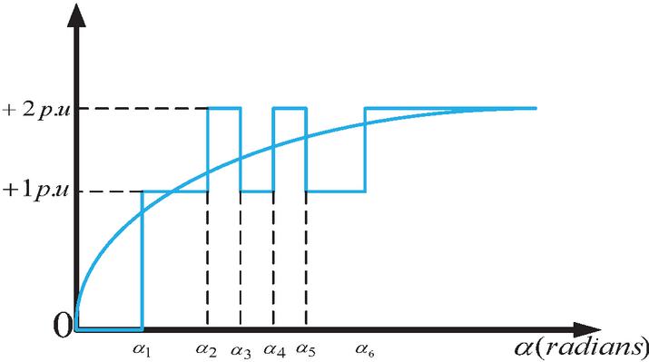
Figure 1 Symmetrically defined five level MSHE–PWM waveform for a distribution ratio of 1/5 (m 5, k 1 and N k m 6).
2 Proposed CG Based Five-Level Reduced Switch TLI Topology
The proposed inverter topology aims to achieve full LC suppression while naturally facilitating boost in output voltage, rendering it suitable for both off-grid and on-grid load systems.
2.1 Suggested Inverter Configuration
Figure 2 demonstrates the suggested reduced switch CG-five level (CG-5L) TLI circuit configuration, which comprises of a dc input source (Vdc), seven IGBT switches (S1–S7), two switched capacitors (C1 and C2), a single diode (D1) and a load at the output. The suggested inverter produces five output voltage levels, comprising of Vdc, 0 and 2Vdc. As illustrated in Figure 2, the periodic charging of capacitor C1 and C2 is achieved through switches S1 and S5. In particular, capacitor C1, in conjunction with the dc source and switches S2, S3, S6, facilitates the production of a 2Vdc voltage level across the output terminal BN, thereby achieving voltage boosting.
The switching states of all the associated switches, the corresponding voltage levels at the output, and the discharging () or charging () behaviour of the capacitors across various operating modes are all summarized in Table 1. The switched capacitor mechanism inherently self-balances the voltages across capacitors C2 and C1 at 2Vdc and Vdc respectively. Consequently, no additional control technique or current/voltage sensors are needed to regulate the voltage of the capacitors.
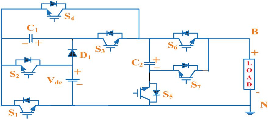
Figure 2 Proposed reduced switch CG-5L TLI topology.
Table 1 Switching states and status of capacitor
| Capacitor Status | ||||||||||
| Modes | ||||||||||
| A | 1 | 0 | 0 | 1 | 0 | 0 | 1 | |||
| B | 0 | 1 | 0 | 1 | 0 | 0 | 1 | – | ||
| C | 0 | 1 | 1 | 0 | 1 | 0 | 1 | |||
| D | 1 | 0 | 1 | 0 | 0 | 1 | 0 | – | ||
| E | 0 | 1 | 1 | 0 | 1 | 1 | 0 | |||
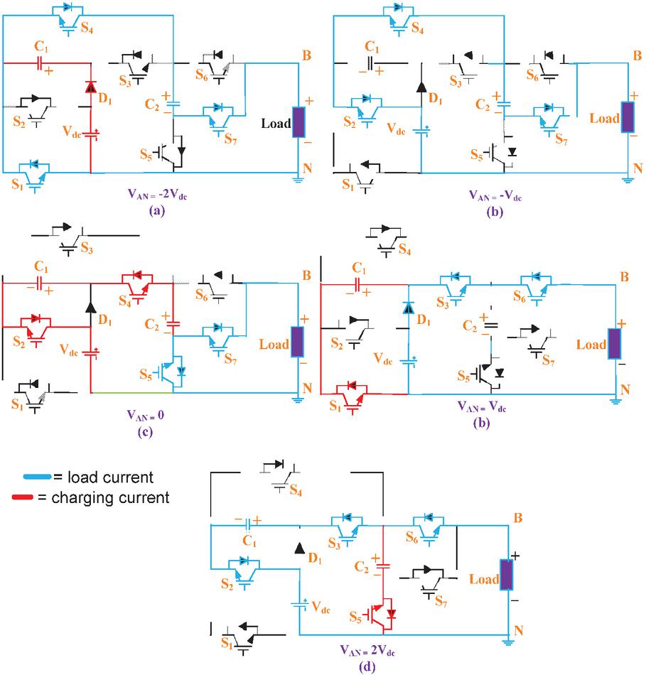
Figure 3 Modes of operation of the suggested reduced switch CG-5L-TLI topology, including capacitor charging path: (a) VBN 2Vdc, (b) VBN -Vdc, (c) VBN 0, (d) VBN Vdc, (e) VBN 2Vdc.
2.2 Modes of Operation of Proposed Topology
The different modes of operation for the suggested inverter are demonstrated in Figure 3. In The figure the current conduction path to the load is highlighted in green colour and capacitor charging current is shown in red colour.
Mode A Operation: During mode A, the diode D1 and switches S1, S4, S7, are triggered into conduction, while the remaining switches are held in their OFF states. As shown in Figure 3(a), the conducting switches (S1, S4, S7) establish a current path through which capacitor (C2) discharges. Consequently, the voltage (VBN) at the output terminal attains a magnitude of 2Vdc, and while capacitor C1 simultaneously, gets charged to a voltage equal input dc source Vdc, driven by the switching action of S1.
| (1) |
Mode B Operation: During mode B, switches S2, S4, and S7 are turned ON while the rest of the switches are held in their OFF states, as illustrated in Figure 3(b). The simultaneous conduction of these three switches S2, S4, and S7 establishes a current path that discharges the capacitor C2 towards the load terminal. As a result, the capacitor C2 and dc input source appear in series combination, producing an output voltage (VBN) equal to Vdc.
| (2) |
Mode C Operation: During Mode C, switches S2, S3, S5, and S7 are brought into conduction while the rest are held in their OFF states, as illustrated in Figure 3(c). The conduction of these switches establishes a path through which capacitor C1 discharges into capacitor C2, driving the output voltage (VBN) to zero
| (3) |
Mode D Operation: During Mode D, switches S1, S3, S5, and diode D1 are triggered into conduction, while the remaining switches are held in their OFF states, as illustrated in Figure 3(d). Through the switching action of S1, capacitor C1 gets charged to Vdc. At the same time, the input voltage source establishes a direct connection to the output terminal via diode D1 and switches S3 and S5, producing an output voltage (VBN) equals to Vdc.
| (4) |
Mode E Operation: During this mode, switches S2, S3, S5, and S6 are brought into conduction, while all remaining switches are held in their OFF states, as depicted in Figure 3(e). In this mode, capacitor C1 undergoes discharging, while capacitor C2 gets connected in parallel across the series combination of Vdc and VC1 via switch S5, charging it to 2Vdc. Furthermore, the VBN at the output attains a magnitude of 2Vdc, which corresponds to the sum of the input voltage source and the voltage across capacitor C1.
| (5) |
3 MSHE–PWM Strategy for Five-Level Output Waveform
The symmetrical structured MSHE–PWM technique for five-level output waveform proposed in paper [30] is based on the line-to-neutral voltage, as illustrated in Figure 1. In this modulation strategy, the output voltage is synthesized using five symmetrically distributed voltage levels, namely 2 p.u., 0, 1 p.u., within one fundamental cycle. The total number of switching transitions defined within one quarter of the waveform period is denoted by N, which may be selected as either an odd or an even integer, subject to specific structural constraints. In this paper, N is chosen as an even integer. Let k denote the number of switching transitions between the 0 p.u. and 1 p.u. voltage levels. Since the first transition occurs from 0 p.u. to 1 p.u., k is necessarily odd. Let m represent the remaining switching transitions between the 1 p.u. and 2 p.u. voltage levels. This number can be either even or odd depending upon N. For the case where N is even and k is odd, m is also constrained to be odd, thereby restricting the total number of switching transitions N to an even value.
| (6) |
For a given modulation ratio (k/m), the method requires the formulation of a specific set of transcendental equations derived from the Fourier series representation of the output voltage to selectively eliminate targeted harmonic components. The approach adheres the classical SHE–PWM principle, whereby the switching angles are computed to simultaneously regulate the fundamental output component and suppress targeted harmonics. Although this formulation was originally developed for a five-level multilevel waveform, preserving both half-wave and quarter-wave symmetries, the same theoretical framework is adopted in this paper. Accordingly, once the switching angles are obtained within the interval 0 to , the remaining angles over the fundamental period are determined using half wave symmetry. With N switching angles employed, up to (N 1) harmonic components can theoretically be eliminated, provided that valid solutions to the resulting equations exist. As depicted in Figure 4, multiple switching transitions can be realized for same set of switching angles.
In the generalized case, the harmonic elimination problem is represented by the following system of equations, which must be solved to determine the corresponding switching angles.
| (7) | |
| (8) | |
| (9) |
Where
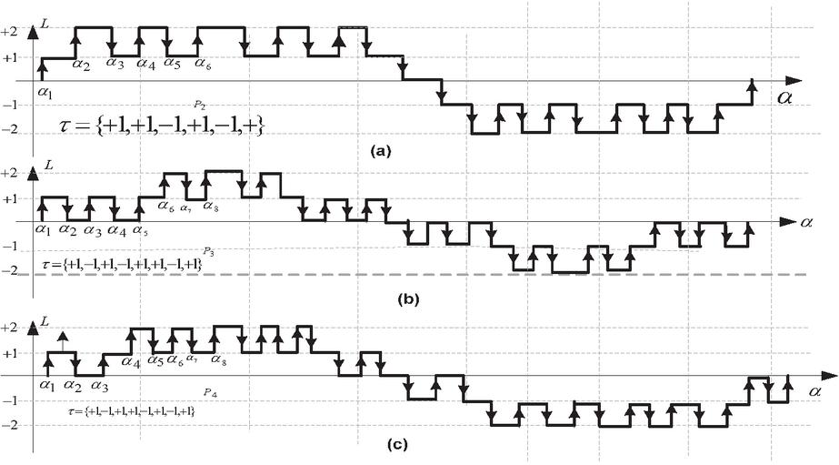
Figure 4 Switching Transitions (a) k 1/5 case, (b) k 5/3 case, (c) k 3/5 case.
If the amplitude of the fundamental component to be produced is V1, then
| (10) |
Where M 2, the square-waveform of 2 p.u. amplitude yields a maximum value at fundamental frequency value of 8/ per unit. The Bayesian minimization technique is applied to solve the transcendental equations describing the Fourier series coefficient. The constraints imposed on the sought solutions are as follows:
4 Bayesian Optimization–Based Selective Harmonic Elimination for a Transformerless Five-Level Inverter
4.1 Bayesian Optimization–Based SHE Methodology
SHE is a widely adopted modulation technique for MLIs, where switching angles are chosen such that specific low-order harmonics are eliminated while maintaining the desired fundamental component. In transformerless five-level inverters, this problem becomes more challenging due to stringent harmonic and leakage-current constraints. The nonlinear relationship between switching angles and harmonic magnitudes results in a highly nonconvex optimization problem that is difficult to solve using classical numerical methods.
For a five-level inverter utilizing eight or six switching angles in the first quarter cycle, these switching angles uniquely define the output voltage waveform and corresponding harmonic spectrum. Since the harmonic amplitudes must be evaluated using Fourier analysis or simulation, analytical gradients of the objective function with respect to switching angles are unavailable. Consequently, the SHE problem is reformulated as a black-box, derivative-free optimization problem.
In this work, Bayesian optimization is utilized because of its well-established effectiveness in addressing computationally expensive black-box optimization problems. In contrast to population-based heuristic methods, Bayesian optimization develops a probabilistic surrogate model of the objective function, which is utilized to intelligently direct the search toward optimal switching angles.
4.2 Objective Function Formulation
The objective function is constructed to penalize both the deviation of the fundamental component from its reference value and the magnitudes of selected low-order harmonics. Minimization of this objective corresponds to a valid SHE solution. This formulation avoids explicit solution of transcendental equations and allows near-optimal solutions to be accepted when exact harmonic elimination is infeasible.
Let the switching-angle vector be defined as:
| (11) |
subject to the constraints
The modulation index (MI) constraint is enforced using the generalized fundamental expression given in (11), which has already been derived and discussed in the preceding section. Selective elimination of low-order harmonics is achieved by enforcing the classical SHE harmonic conditions [1, 4]:
| (12) |
Instead of explicitly solving the resulting system of nonlinear transcendental equations, the SHE problem is reformulated as an optimization problem by minimizing the squared residuals of the fundamental and harmonic equations, as commonly adopted in modern SHE formulations [4]. Accordingly, the objective function is defined as:
| (13) |
Where H {3, 5, 7, 9, 11} denotes the set of harmonics to be eliminated. Minimization of J() is mathematically equivalent to solving the original SHE equations when an exact solution exists and provides the best achievable approximation otherwise.
4.3 Gaussian Process Surrogate Modelling
In Bayesian optimization, the objective function defined in (13) is treated as an expensive black-box function and is modelled using a Gaussian Process () surrogate. Based on a finite set of evaluated switching-angle samples, the provides a probabilistic prediction of the objective function at unexplored points. Specifically, it yields both the expected value and the associated uncertainty. A defines a distribution over functions and is fully characterized by a mean function and a covariance function, expressed as:
A squared exponential kernel is employed in this work due to its smoothness and generalization capability, and is given by [5, 6]:
| (14) |
Where the signal variance and is a diagonal matrix of length-scale parameter.
Given a set of evaluated switching-angle samples , the provides a predictive distribution for any unexplored point , characterized by a mean and variance . This probabilistic prediction captures both the expected objective value and the associated uncertainty.
This probabilistic modelling approach proves advantageous for SHE, as it allows the optimizer to locate promising regions within the switching-angle space while simultaneously quantifying confidence in the predictions. Regions of high uncertainty are systematically explored to avoid overlooking feasible solutions, while regions associated with low predicted cost are exploited to refine the optimal switching angles. The probabilistic surrogate model provides both the predicted objective value and the associated uncertainty estimate, which proves particularly advantageous in addressing the highly nonlinear characteristics of the SHE problem.
4.4 Acquisition Function and Switching-Angle Selection
An acquisition function is employed to determine the next switching-angle candidate to be evaluated. In this work, the Expected Improvement (EI) criterion is adopted. EI quantifies the expected reduction in the objective function relative to the best solution obtained so far.
The EI acquisition function is employed to direct the selection of new switching-angle candidates. EI is defined as:
| (15) |
Where, Jmin denotes the minimum objective value. For a Gaussian predictive with standard distribution and mean , the EI function can be expressed analytically as [6]:
| (16) |
Where, and denote the cumulative distribution function and probability density function of the standard normal distribution, respectively.
By maximizing (15), the Bayesian optimization framework balances exploitation and exploration in a mathematically principled manner, yielding smooth and continuous switching-angle trajectories with respect to the MI, which is highly desirable for practical SHE implementation. By applying Bayesian optimization, the switching angles corresponding to various MIs are tabulated in Tables 2 and 3. Table 2 presents eight switching angles ( to ) for eight switching transitions, while Table 3 presents six switching angles ( to ) for six switching transitions. The flow chart for the Bayesian optimisation technique is illustrated below in Figure 5.
Table 2 Calculated notch angles ( to ) corresponding to various MIs for eight switching transitions
| MI | ||||||||
| 0.4 | 0.199 | 0.27135 | 0.4235 | 0.59214 | 0.66939 | 1.22076 | 1.27805 | 1.53137 |
| 0.5 | 0.240 | 0.37182 | 0.48678 | 1.01941 | 1.11495 | 1.32337 | 1.47833 | 1.57033 |
| 0.6 | 0.232 | 0.3584 | 0.4689 | 0.96995 | 1.05764 | 1.23741 | 1.37052 | 1.50217 |
| 0.7 | 0.173 | 0.2624 | 0.37347 | 0.83762 | 0.95661 | 1.10764 | 1.33501 | 1.42679 |
| 0.8 | 0.203 | 0.33610 | 0.3975 | 0.66544 | 0.74402 | 0.88787 | 1.08239 | 1.13769 |
Table 3 Calculated notch angles ( to ) corresponding to various MIs for six switching transitions
| MI | ||||||
| 0.4833 | 0.3022 | 0.47654 | 0.61443 | 1.31872 | 1.40361 | 1.5704 |
| 0.50 | 0.29133 | 0.45828 | 0.59021 | 1.2285 | 1.30108 | 1.53186 |
| 0.5518 | 0.24367 | 0.37513 | 0.50455 | 1.11519 | 1.23017 | 1.48842 |
| 0.5973 | 0.00877 | 0.16983 | 0.407 | 1.05639 | 1.21706 | 1.4542 |
| 0.8012 | 0.24608 | 0.60947 | 0.65725 | 0.70821 | 0.91378 | 1.03325 |
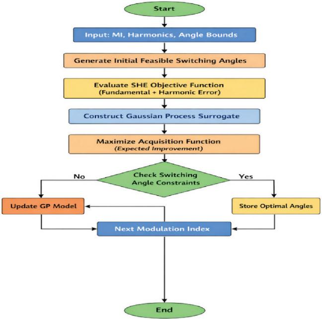
Figure 5 Flowchart illustrating working if Bayesian optimization algorithm.
Particle Swarm Optimization and Genetic Algorithms have been widely used for SHE due to their simplicity and flexibility. However, these methods rely on population-based random search mechanisms, which often require a large number of function evaluations and careful tuning of algorithmic parameters.
In contrast, Bayesian optimization uses a probabilistic surrogate model to guide the search process. As a result, it converges with significantly fewer objective-function evaluations. Moreover, PSO and GA are stochastic in nature and may produce different solutions in different runs, whereas Bayesian optimization is deterministic for a given kernel and initialization.
A notable benefit of Bayesian optimization is the continuity of the resulting switching-angle trajectories. Population-based methods often exhibit discontinuities in angle trajectories as the MI varies, which complicates real-time implementation. Bayesian optimization inherently yields smooth and continuous trajectories, rendering it more appropriate for practical SHE applications.
The Bayesian optimization framework offers a systematic and efficient methodology for SHE switching-angle computation. By integrating probabilistic modelling with intelligent sampling, it overcomes the limitations of classical numerical solvers and population-based heuristics. The method is particularly suitable for transformerless MLIs, where harmonic performance, repeatability, and computational efficiency are critical importance.
Figure 6 show the optimal switching angles obtained using the Bayesian optimization technique plotted against different values of MI for the k 3/5 case, corresponding to six and eight switching transitions, respectively.
From the figures, it is evident that the optimum solution set in both cases, comprising the respective switching angles, converges to lower values as the MI increases. The switching angles , , , , , , , and represent the optimal notch angles computed at each value of the MI.
Figure 7 illustrates the optimal switching angles computed for various MIs in the k 3/3 case, while Figure 8 presents the corresponding harmonic profiles at different MIs.
Similarly, Figure 10 demonstrates the optimal switching angles computed for various MIs in the k 5/3 case, While Figure 11 shows the corresponding harmonic profile at different MIs.
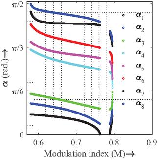
Figure 6 Switching angle vs MI graph for 3/5 case for eight switching transitions.
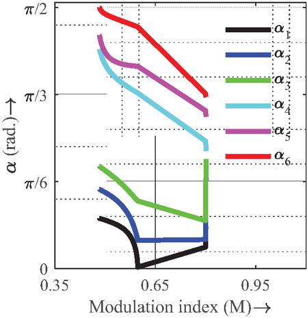
Figure 7 Switching angle vs MI graph index for 3/3 case.
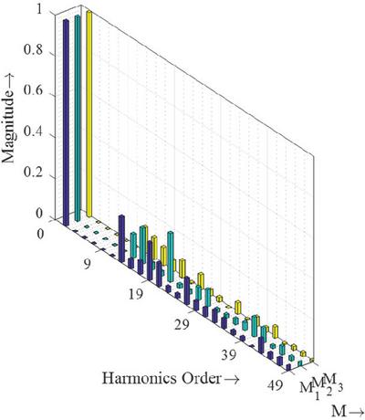
Figure 8 Harmonics profile at different MIs: M, M and M for 3/3 case.
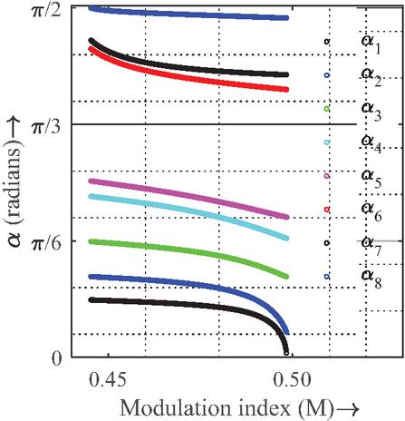
Figure 9 Switching angle vs MI graph for 5/3 case.
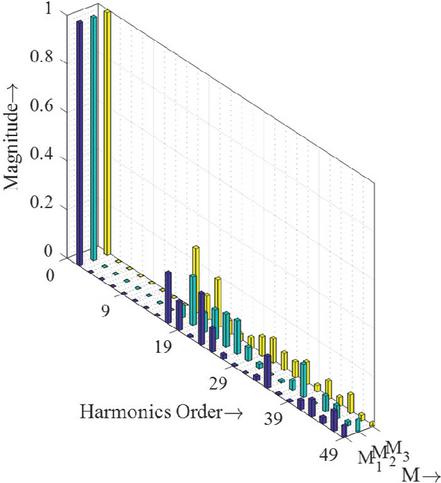
Figure 10 Harmonics profile at different MIs: M, M, M for 5/3 case.
As observed from the Figures 9 and 10, the fundamental component dominates with the highest magnitude in all cases. The effectiveness of the adopted switching strategy is seen clearly in the notable suppression of the lower-order odd harmonics, particularly in the SHE cases. The magnitude of higher-order harmonics shows progressive reduction which indicates distortion at higher harmonic orders is diminished. Overall, increasing the number of switching transitions gives a significant improvement in harmonic performance, illustrating the benefits of higher-order switching patterns in producing a cleaner spectrum output voltage.
5 Simulation and Experimental Results
To validate the performance of the suggested TLI topology, both simulation and experimental analyses are carried out. Furthermore, a reduced scale laboratory setup is built to demonstrate the practical viability and operational capability of the suggested inverter.. The key performance aspects evaluated include validation under various load conditions and generation of a high-quality five-level output waveform with reduced harmonic distortion. Table 4 summarizes the key parameters employed in the simulation and experimental studies.
Table 4 Experimental and simulation parameters
| Parameters | Experimental | Simulation |
| Dc input supply | 20V | 20 V |
| Output frequency | 50 Hz | 50 Hz |
| Output voltage | 32.05V (RMS) | 32.05 V (RMS) |
| Capacitors (C1 and C2) | C F | C F |
| C F | C F | |
| IGBT | FG25N120 (1200V/50A) | – |
| Diode | 25D40R (400/25) | – |
| OPAL-RT 4510 | OPAL-RT 4510 | – |
5.1 Simulation Results
A Five-level SHE PWM output waveform with eight or six switching angle sought within the quarter period is synthesized by an TLI voltage source inverter. In the MATLAB simulation, different switching patterns are adopted to obtain the high quality output voltage waveform. The switching patterns employed are k 1/5, k 3/5, and k 5/3. The analysis is carried out at different MIs, namely MI 0.8, 0.55, and 0.48. The calculated switching angles corresponding to various MIs for eight and six switching transitions are presented in Tables 2 and 3, respectively, and are employed in the simulation. The TLI is supplied by a 20 V dc source and operates at a fundamental frequency of 50 Hz.
Figure 11 illustrates the output voltage waveform in which eight switching transitions (k 5/3) are achieved within a quarter period of the waveform. At MI 0.80, the expected RMS value of the fundamental component of the output voltage is 26.05 V. At the MI 0.80, the proposed topology is simulated under different load conditions, including inductive, resistive and dynamic loads.
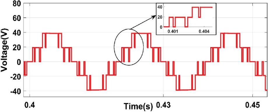
Figure 11 Waveform of output voltage with MI 0.8 and k 5/3.
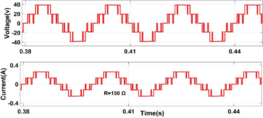
Figure 12 Waveforms of current and voltage for R-Load.
Figure 12 depicts the waveform of the output current and voltage corresponding to a load that is resistive in nature (R 150 ). Since the load is resistive, hence no phase displacement exists between the current and voltage waveforms. Figure 13 depicts the inverter behaviour for an RL load with a visible phase displacement existing among the current and voltage waveforms because of inductance. The value of R used is 150 and the value of L used is 150 mH. Figure 14 presents the inverter behaviour under dynamic load conditions, with the load transitioning from Z1 comprising resistance of 200 and inductance of 200 mH to Z2, comprising a resistance of 150 to inductance of 150 mH. Despite the phase displacement introduced by the inductive component, the output waveforms remain well-regulated and stable, reflecting the adaptability and robustness of the proposed topology to varying load profiles.
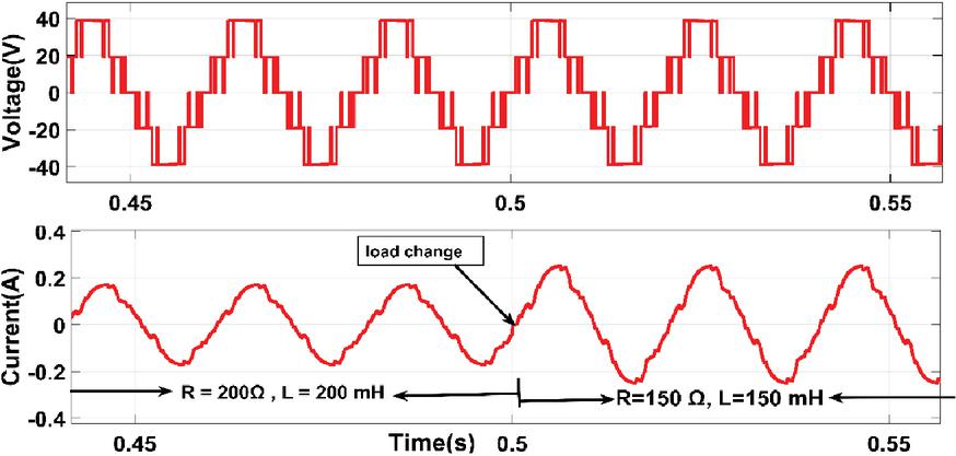
Figure 13 Waveforms of current and voltage for RL-Load.
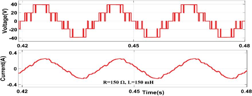
Figure 14 Waveforms of current and voltage during dynamic RL-load transition.
The output voltage waveforms corresponding to six (k 1/5) switching transitions sought within a quarter period of the waveform are shown in Figure 15 and Figure 16 at MI 0.80 and MI 0.60, respectively. Furthermore, an additional switching pattern is adopted, as illustrated in Figure 17. In this switching pattern, eight (k 3/5) switching transitions are achieved within a quarter period of the waveform at a MI 0.50. The leakage current is shown in Figure 18.
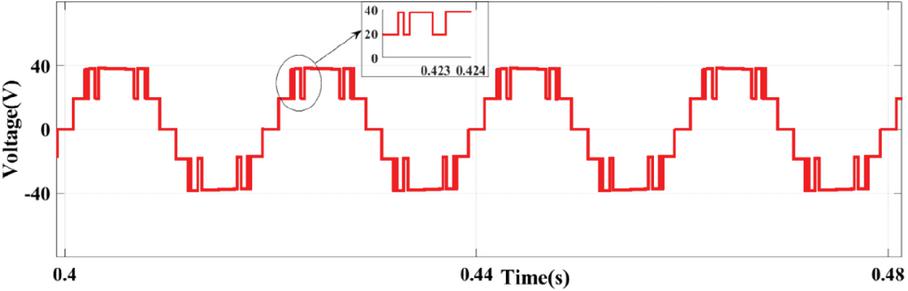
Figure 15 Waveform of output voltage with MI 0.8 and k 1/5.
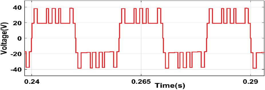
Figure 16 Waveform of output voltage with MI 0.55 and k 1/5.
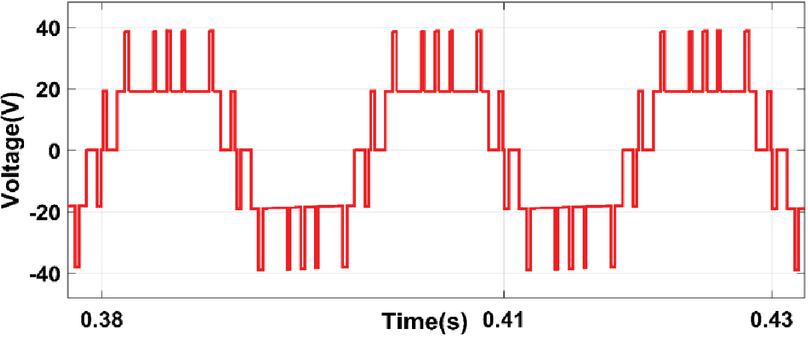
Figure 17 Waveform of output voltage with MI 0.488 and k 3/5.
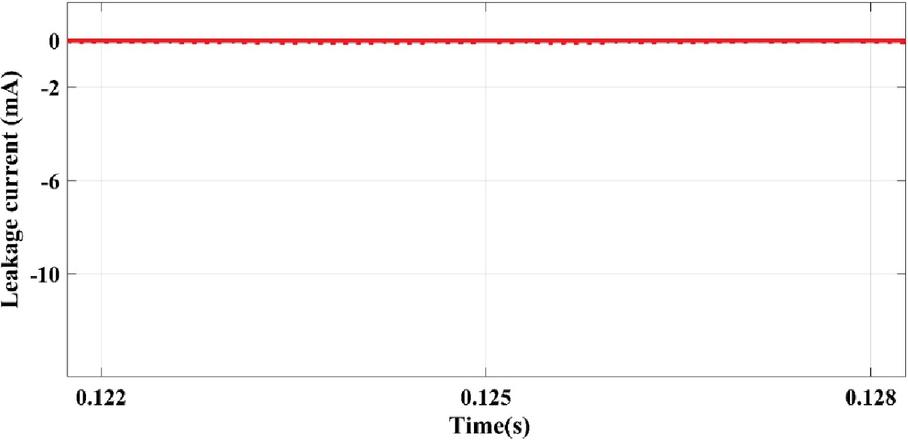
Figure 18 Waveform of leakage current.
5.2 Experimental Results
Besides simulation analysis, the practical performance of the proposed TLI topology is also evaluated on a scaled-down laboratory setup, and the parameters used in the experimental setup are listed in Table 3. Figure 19 depicts the experimental test setup. The prototype comprises a dc supply, a diode (25D40R), seven IGBT switches (FGA25N120), seven gate drivers (TLP250), two capacitors (C F and C F) and RL load. The other key instruments used are PQ analyser, DSO and OPAL-RT. The OPAL-RT 4510 generating gate pulses which are amplified by gate driver circuits hence acts as main controller. The input to the inverter is provided by 30V dc supply, and the system is operated at a switching frequency of 50 Hz. The performance is evaluated under various switching transition and load conditions, where different switching patterns are adopted to obtain the high quality output voltage waveform.
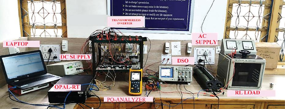
Figure 19 Hardware setup of proposed topology.
Figure 20(a) shows the output voltage generated using the NLC technique, and Figure 20(b) shows the corresponding voltage THD. The voltage THD at a MI of 0.80 is 35.8%. The predominant harmonics present are odd harmonics, namely the 3rd, 5th, 7th, 9th, 11th, 15th, and 17th orders. Additionally, from the figure it is observed that twice voltage boosting is achieved, as the output voltage levels of 40 V is obtained corresponding to an input voltage of 20 V.
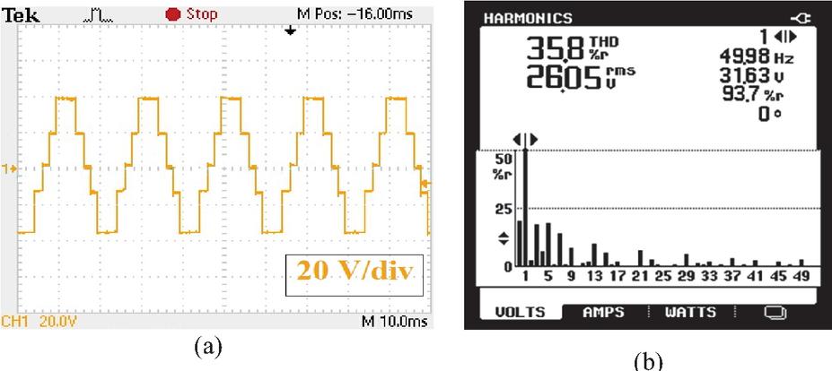
Figure 20 Waveform of output voltage and harmonic analysis using NLC technique (a) Output voltage with MI 0.8, (b) Voltage THD at with MI 0.8.
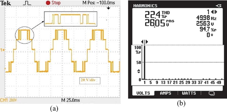
Figure 21 Waveform of output voltage and harmonic analysis using SHE technique. (a) Output voltage with MI 0.8 and k 1/5, (b) Voltage THD at k 1/5 and MI 0.8.
Figure 21(a) illustrates the output voltage waveform in which six (k 1/5) switching transitions are sought within a quarter period of the waveform. The value of switching angles used in this case against MI 0.8 are: , , , , , . From Figure 21(a) it is depicted that the five switching transition are performed between 20 V and 40 V voltage levels and the remaining one is done between 0 V and 20 V voltage level. The value of Figure 21(b) shows the corresponding voltage THD at MI 0.8, from which it is observed that five odd harmonics, corresponding to harmonic orders 3rd, 5th, 7th, 9th, and 11th, are successfully eliminated. This results in a reduced THD of 22.4% at the same MI employed for the NLC technique. The rms value of fundamental component is 26.05 V, which comprises of 94.7% of total voltage value. Figure 22 depicts the inverter behaviour for RL load comprising a resistance of 150 and an inductance of 150 mH, where a visible phase displacement between the current and voltage waveforms is observed owing to the inductive component. Figure 23 presents the inverter performance under a dynamic load condition, in which the load transitions from Z1, comprising a resistance of 150 and an inductance of 150 mH, to Z2, comprising resistance of 200 and an inductance of 200 mH.
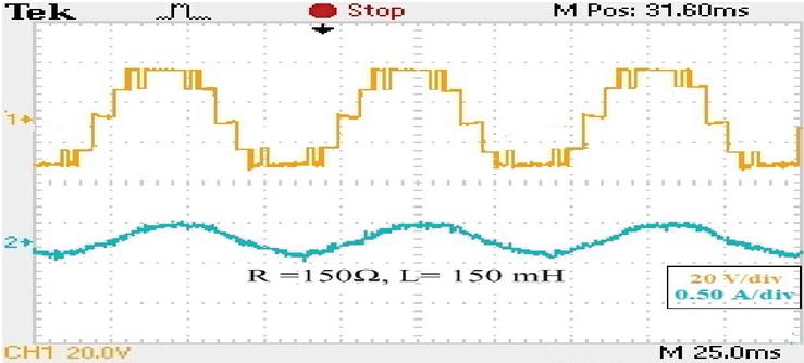
Figure 22 Waveform of current and voltage for RL load.
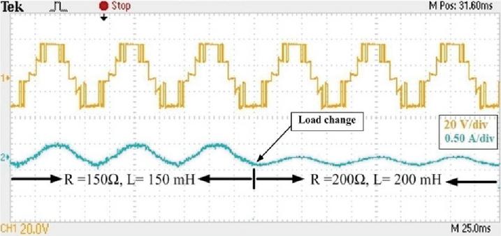
Figure 23 Waveforms of current and voltage during dynamic RL-load transition.
Similarly, Figure 24(a) illustrates the output voltage waveform in which eight (k 5/3) switching transitions are sought within a quarter period of the waveform. The value of eight switching angles used in this case against MI 0.8 are: , , , , , , , . From Figure 24(a) it is depicted that the three switching transition are performed between 20 V and 40 V voltage levels and the remaining five is done between 0 V and 20 V voltage level.
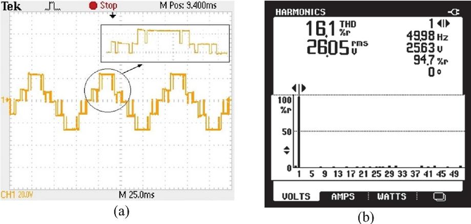
Figure 24 Waveform of output voltage and harmonic analysis using SHE technique (a) Output voltage with MI 0.8 and k 5/3, (b) Voltage THD at k 5/3 and MI 0.8.
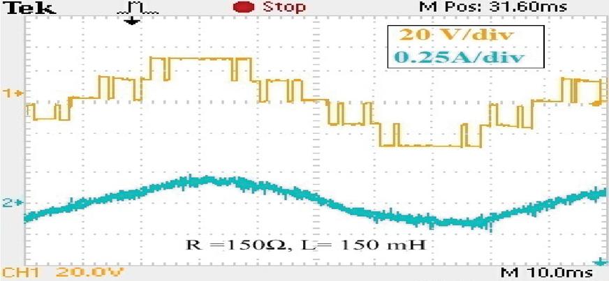
Figure 25 Waveform of current and voltage for RL-Load.
Figure 24(b) depicts the voltage THD at MI 0.8. From the FFT analysis, it is observed that eight harmonics, corresponding to harmonic orders 3rd, 5th, 7th, 9th, 11th, 13th, and 15th, are eliminated. This further reduces the THD to 16.1%. The rms value of fundamental component is 26.05 V, which comprises of 94.7 % of total voltage value. Additionally, for the eight (k 5/3) switching transitions, the inverter performance under both RL and dynamic load conditions was evaluated. Figure 25 presents the inverter behaviour for an RL load. The value of resistance used is 150 and value of an inductance is 150 mH. Figure 26 presents the inverter performance under a dynamic load condition, in which the load transitions from Z1, comprising a resistance of 150 and an inductance of 150 mH, to Z2, comprising resistance of 200 and an inductance of 200 mH.
Figure 27 illustrates the output voltage waveform corresponding to eight (k 3/5) switching transitions within a quarter period of the waveform. In this case, MI equal to 0.5 is employed. The value of eight switching angles used in this case against MI 0.488 are: , , , , , , , . From Figure 27 it is depicted that the five switching transition are performed between 20 V and 40 V voltage levels and the remaining three is done between 0 V and 20 V voltage level.
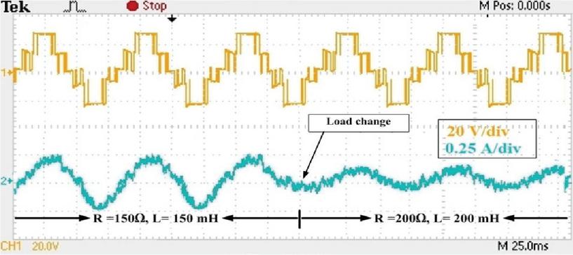
Figure 26 Waveforms of current and voltage during the dynamic RL-Load.
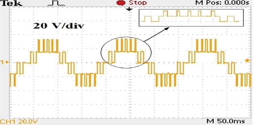
Figure 27 Waveform of output voltage with MI 0.488 and k 3/5.
6 Conclusion
In this paper, a CG-5L TLI topology with reduced-switch is suggested and evaluated under various load conditions. Since the CG configuration is adopted, leakage current is completely eliminated. Additionally, voltage boosting is achieved without the need for an additional boost converter.
This paper implemented a symmetrically defined MSHE–PWM technique to generate a high-quality five-level output waveform with reduced harmonic distortion. The switching angles are determined using a Bayesian optimization method, resulting in an efficient procedure for computing the switching angles. It is demonstrated that the implemented method enables the calculation of switching angles over the entire range of MIs by employing a distribution ratio and systematic solution search. The simulation and experimental results are presented to validate the theoretical analysis.
References
[1] Jih-Sheng Lai and Fang Zheng Peng, “Multilevel converters-a new breed of power converters,” in IEEE Transactions on Industry Applications, vol. 32, no. 3, pp. 509–517, May–June 1996.
[2] R. W. Menzies, P. Steimer and J. K. Steinke, “Five level GTO inverters for large induction motor drives,” Conference Record of the 1993 IEEE Industry Applications Conference Twenty-Eighth IAS Annual Meeting, Toronto, ON, Canada, 1993, pp. 595–601 vol. 1.
[3] Jie Zhang, “High performance control of a three-level IGBT inverter fed AC drive,” IAS ’95. Conference Record of the 1995 IEEE Industry Applications Conference Thirtieth IAS Annual Meeting, Orlando, FL, USA, 1995, pp. 22–28 vol. 1.
[4] Mohammed LA, Husain TA, Ibraheem AMT. Implementation of SHE-PWM technique for single-phase inverter based on Arduino. Int J Electr Comput Eng. 2021;11(4):2907.
[5] Ghoudelbourk S, Azar AT, Dib D, Omeiri A. Selective harmonic elimination strategy in multilevel inverters for grid-connected photovoltaic systems. Int J Adv Intell Paradigms. 2020;15(3):317.
[6] M. S. A. Dahidah, G. Konstantinou and V. G. Agelidis, “A Review of Multilevel Selective Harmonic Elimination PWM: Formulations, Solving Algorithms, Implementation and Applications,” in IEEE Transactions on Power Electronics, vol. 30, no. 8, pp. 4091–4106, Aug. 2015
[7] H. S. Patel and R. G. Hoft, “Generalized Techniques of Harmonic Elimination and Voltage Control in Thyristor Inverters: Part I–Harmonic Elimination,” in IEEE Transactions on Industry Applications, vol. IA-9, no. 3, pp. 310–317, May 1973.
[8] T. Kato, “Precise PWM Waveform Analysis of Inverter for Selected Harmonic Elimination,” 1986 Annual Meeting Industry Applications Society, Denver, CO, USA, 1986, pp. 611-616.
[9] T. Kato, “Sequential homotopy-based computation of multiple solutions for selected harmonic elimination in PWM inverters,” in IEEE Transactions on Circuits and Systems I: Fundamental Theory and Applications, vol. 46, no. 5, pp. 586–593, May 1999,
[10] J. N. Chiasson, L. M. Tolbert, K. J. McKenzie and Zhong Du, “A complete solution to the harmonic elimination problem,” in IEEE Transactions on Power Electronics, vol. 19, no. 2, pp. 491–499, March 2004
[11] Salman Ahmad, Mohammed Meraj, Atif Iqbal, Imtiaz Ashraf, Selective harmonics elimination in multilevel inverter by a derivative-free iterative method under varying voltage condition, ISA Transactions, Volume 92, 2019, Pages 241–256, ISSN 0019-0578.
[12] V. G. Agelidis, A. Balouktsis and I. Balouktsis, “On applying a minimization technique to the harmonic elimination PWM control: the bipolar waveform,” in IEEE Power Electronics Letters, vol. 2, no. 2, pp. 41–44, June 2004, doi: 10.1109/LPEL.2004.831157.
[13] F. Swift and A. Kamberis, “A new Walsh domain technique of harmonic elimination and voltage control in pulse-width modulated inverters,” in IEEE Transactions on Power Electronics, vol. 8, no. 2, pp. 170–185, April 1993.
[14] Tsorng-Juu Liang, R. M. O’Connell and R. G. Hoft, “Inverter harmonic reduction using Walsh function harmonic elimination method,” in IEEE Transactions on Power Electronics, vol. 12, no. 6, pp. 971–982, Nov. 1997.
[15] J. R. Wells, B. M. Nee, P. L. Chapman and P. T. Krein, “Optimal harmonic elimination control,” 2004 IEEE 35th Annual Power Electronics Specialists Conference (IEEE Cat. No.04CH37551), Aachen, Germany, 2004, pp. 4214–4219, Vol. 6.
[16] Ahmad S, Iqbal A, Ashraf I, Ganie ZA. Harmonics minimization in multilevel inverter by continuous mode ACO technique. In: Metaheuristic and Evolutionary Computation: Algorithms and Applications. Singapore: Springer; 2021.
[17] B. Ozpineci, L. M. Tolbert and J. N. Chiasson, “Harmonic optimization of multilevel converters using genetic algorithms,” 2004 IEEE 35th Annual Power Electronics Specialists Conference (IEEE Cat. No.04CH37551), Aachen, Germany, 2004, pp. 3911–3916 Vol. 5.
[18] M. S. A. Dahidah and V. G. Agelidis, “A Hybrid Genetic Algorithm for Selective Harmonic Elimination Control of a Multilevel Inverter with Non-Equal DC Sources,” 2005 International Conference on Power Electronics and Drives Systems, Kuala Lumpur, Malaysia, 2005, pp. 1205–1210.
[19] M. Kumari et al., “Genetic Algorithm based SHE-PWM for 1-ø and 3-ø Voltage Source Inverters,” 2019 International Conference on Power Electronics, Control and Automation (ICPECA), New Delhi, India, 2019, pp. 1–6,
[20] V. G. Agelidis, A. Balouktsis, I. Balouktsis and C. Cossar, “Multiple sets of solutions for harmonic elimination PWM bipolar waveforms: analysis and experimental verification,” in IEEE Transactions on Power Electronics, vol. 21, no. 2, pp. 415–421, March 2006.
[21] J. R. Wells, B. M. Nee, P. L. Chapman and P. T. Krein, “Selective harmonic control: a general problem formulation and selected solutions,” in IEEE Transactions on Power Electronics, vol. 20, no. 6, pp. 1337–1345, Nov. 2005.
[22] Jabr RA. Solution trajectories of the harmonic-elimination problem. Proc Inst Electr Eng. 2006;153:97–104.
[23] Li Li, D. Czarkowski, Yaguang Liu and P. Pillay, “Multilevel selective harmonic elimination PWM technique in series-connected voltage inverters,” in IEEE Transactions on Industry Applications, vol. 36, no. 1, pp. 160–170, Jan.–Feb. 2000,
[24] Z. Du, L. M. Tolbert and J. N. Chiasson, “Harmonic elimination for multilevel converter with programmed PWM method,” Conference Record of the 2004 IEEE Industry Applications Conference, 2004. 39th IAS Annual Meeting., Seattle, WA, USA, 2004, pp. 2210–2215 vol. 4.
[25] J. Vassallo, J. C. Clare and P. W. Wheeler, “A power-equalized harmonic-elimination scheme for utility-connected cascaded H-bridge multilevel converters,” IECON’03. 29th Annual Conference of the IEEE Industrial Electronics Society (IEEE Cat. No.03CH37468), Roanoke, VA, USA, 2003, pp. 1185–1190 Vol. 2.
[26] J. Holtz, W. Lotzkat and K. -H. Werner, “A high-power multi transistor-inverter uninterruptable power supply system,” 1986 17th Annual IEEE Power Electronics Specialists Conference, Vancouver, BC, Canada, 1986, pp. 311–320.
[27] V. G. Agelidis, A. Balouktsis, C. Cossar and I. Balouktsis, “Five-Level Selective Harmonic Elimination PWM Strategies and Multicarrier Phase-Shifted Sinusoidal PWM: A Comparison,” 2005 IEEE 36th Power Electronics Specialists Conference, Dresden, Germany, 2005, pp. 1685–1691.
[28] Zhong Du, L. M. Tolbert and J. N. Chiasson, “Active harmonic elimination for multilevel converters,” in IEEE Transactions on Power Electronics, vol. 21, no. 2, pp. 459–469, March 2006.
[29] V. G. Agelidis, A. I. Balouktsis and M. S. A. Dahidah, “A Five-Level Symmetrically Defined Selective Harmonic Elimination PWM Strategy: Analysis and Experimental Validation,” in IEEE Transactions on Power Electronics, vol. 23, no. 1, pp. 19–26, Jan. 2008.
[30] V. K. Verma, H. K. Meena and S. N, “Selective Harmonic Elimination In 5-Level MLI Using Particle Swarm Optimization,” 2024 Fourth International Conference on Advances in Electrical, Computing, Communication and Sustainable Technologies (ICAECT), Bhilai, India, 2024, pp. 1–5, doi:10.1109/ICAECT60202.2024.104692.
[31] S. Shakeera and K. Rachananjali, “Study of Multilevel Inverter with SHE-PWM Using PSO Algorithm,” 2024 International Conference on Intelligent and Innovative Technologies in Computing, Electrical and Electronics (IITCEE), Bangalore, India, 2024, pp. 1–5, doi:10.1109/IITCEE59897.2024.10467266.
[32] M. Sadoughi, A. Pourdadashnia, M. F.-Kangarlu and S. Galvani, “PSO-Optimized SHE-PWM Technique in a Cascaded H-Bridge Multilevel Inverter for Variable Output Voltage Applications,” in IEEE Transactions on Power Electronics, vol. 37, no. 7, pp. 8065–8075, July 2022, doi:10.1109/TPEL.2022.
[33] H. Taghizadeh and M. T. Hagh, “Harmonic Elimination of Cascade Multilevel Inverters with Nonequal DC Sources Using Particle Swarm Optimization,” in IEEE Transactions on Industrial Electronics, vol. 57, no. 11, pp. 3678–3684, Nov. 2010, doi:10.1109/TIE.2010.2041736.
[34] T. H. Parray and F. I. Bakhsh, “A Novel Reduced Switch Five-Level Common Ground Transformerless Inverter Feeding an Isolated Load” International Journal of Circuit Theory and Applications, 1–16, 2026, https://doi.org/10.1002/cta.70325.
[35] Ahmad S, Ahmad J, Bakhsh FI. “Optimized harmonic PWM implementation in a reduced switch count MLI with quadruple boosting using PSO for solar PV applications,” Eng Res Express. 2025;7(1):015341.
[36] Ahmad, S., Uddin, R., Ganie, Z. A., Anees, A. S., and Bakhsh, F. I. (2022). Low Frequency Operation and dsPIC Micro-controller Implementation for Multilevel Quasi Z Source Inverter in Photovoltaic Application. Distributed Generation & Alternative Energy Journal, 37(4), 929–958.
[37] Husain, M. A., Rajput, R., Gupta, M. K., Tabrez, M., Ahmad, M. W., and Bakhsh, F. I. (2022). Design and Implementation of Different Drive Topologies for Control of Induction Motor for Electric Vehicle Application. Distributed Generation & Alternative Energy Journal, 37(4), 999–1026.
Biographies

Tajamul Hayat Parray was born in Srinagar, J&K, India, in 1996. He received the B.Tech. degree from the University of Kashmir Hazratbal, Srinagar, Zakura campus in 2018 and the M.Tech. degree in power electronics and electrical drives from the National Institute of Technology Srinagar in 2022. He is currently working toward the Ph.D. degree in the Department of Electrical, National Institute of Technology Srinagar. His current research interests include multilevel inverters, grid-connected PV inverters, transformerless inverters, dc-dc switched capacitors and DC converters, and electrical machine drives.

Salman Ahmad received the B.Tech degree in Electrical Engineering from Aligarh Muslim University, Aligarh, India, in 2010 and M.Tech degree from Indian Institute of Technology, Roorkee, India, in 2012, the Ph.D. Degree from Aligarh Muslim University, India in 2020. He is currently an Assistant Professor of electrical engineering with Islamic University of Science and Technology Awantipora, India. He has published more than 25 technical papers in different journals and conference proceedings and contributed three book chapters in edited books published by Elsevier, USA and Springer Nature, Singapore. He received 4 research grants from various government agencies. His current research interests include Power converters, PWM techniques, multilevel and multiphase converter, variable speed drives and renewable energy systems.

Farhad Ilahi Bakhsh (Senior Member, IEEE) received B. Tech degree in Electrical Engineering and M. Tech. degree in Power Systems & Drives from Aligarh Muslim University (AMU), Aligarh, India in 2010 and 2012, respectively. Then he pursued Ph.D. from Indian Institute of Technology Roorkee, India in 2017. During his Ph.D. he developed a new method for grid integration for wind energy generation system which has been recognized worldwide. He developed an automatic solar tracking system which has been appreciated by IEEE India Council, Centre for Embedded Product Design, Centre for Electronics Design and Technology, Netaji Subhas Institute of Technology in association with IEEE Delhi Section & IEEE CAS, Bangalore Chapter. Currently he is serving as Assistant Professor in Department of Electrical Engineering, National Institute of Technology Srinagar, Jammu & Kashmir, India. He is founder and Counselor of IEEE Student Branch, NIT Srinagar.
He has won “10 for 10 Typhoon HIL Award” from Switzerland, Europe. He delivered a number of Keynote talks, Invited talks and Expert Lectures at National and International level in conferences, workshops, STC, etc. He has more than 100 published papers in Scopus or Web of Science based International reputed Journals and Conferences. He has also published many books in Springer, Wiley, IEEE, Scrivener Publishing and River Publishers with more than 20 book chapters. He has been enlightened with “Award of Excellence in Research” by VALLWAY International. Many times, he got best paper awards in International reputed conferences. Moreover, he has Indian, Australian and South African granted patents in his credit. Recently, he has received “Typhoon HIL Best Paper Award Europe 2025”. In this award, they have received a Typhoon HIL 604 Emulator which costs around 50 lakhs INR. He served as Lead Guest Editor in IET Generation, Transmission and Distribution Journal; Lead Guest Editor in IET Power Electronics Journal; Guest Editor in IET Renewable Power Generation Journal; Guest Editor in Frontiers in Energy Research; Guest Editor in Renewable Energy Focus, Elsevier; Guest Editor in Recent Advances in Electrical & Electronic Engineering; and Associate Editor of e-Prime-Advances in Electrical Engineering, Electronics and Energy, Elsevier. His research area of interests includes Performance Analysis and new applications of Variable Frequency Transformer, Application of Power Electronics & Drives in Renewable Energy Systems (Solar & Wind), Multilevel Converters, Multilevel DC-DC DAB Converters, Alternate Energy Vehicles (Electric/Hybrid) and Multi-phase Drives.
Distributed Generation & Alternative Energy Journal, Vol. 41_4, 1079–1112
doi: 10.13052/dgaej2156-3306.4149
© 2026 River Publishers