Crosstalk-Aware Global Routing in VLSI Design by Using a Shuffled Frog-Leaping Algorithm
Apichat Terapasirdsin and Supaporn Kiattisin*
Technology of Information System Management Division, Faculty of Engineering, Mahidol University, Nakhon Pathom, 73170, Thailand
E-mail: supaporn.kit@mahidol.ac.th; apichat.ter@student.mahidol.ac.th
*Corresponding Author
Received 02 November 19; Accepted 02 June 2020; Publication 17 August 2020
Abstract
Nowadays, very large scale integrated (VLSI) circuit technology is developing rapidly. It is necessary to consider many factors related to the VLSI circuit design. Interference is one of the factors that must be considered in high-frequency systems. The parasitic elements become serious limiting factors in the circuit. This research provided a method to reduce crosstalk energy by considering the transition of the signal. Crosstalk is the main capacitive effect which is elected by a high-coupling capacitance between lines. This study considers the wiring path signal with disturbance using the theory of optimization model, assisting in the search of the best sort in signal lines. The technique of a shuffled frog leaping algorithm (SFLA) is being used to search for the best value in arranged signal lines. The result will be minimal noise. The study finds that the arrangement using the SFLA causes only 36.42% of the noise. It was initially evident and 13.06%, when compared with the average all, is born noise value. These techniques can be applied in the design of arranging signal line in the VLSI circuits.
Keywords: Optimization, crosstalk, shuffled frog leaping, signal coupling.
1 Introduction
VLSI technology has been continuously developed in recent years, which resulted in effective VLSI circuits and smaller circuit sizes [1]. The integration of density is increasing in deep submicron (DSM) design. Design contribution is the approximation of crosstalk between adjacent wires on the layer. Increasing crosstalk results in terms of noise and delay, which is called the parasitic effect. There are important criteria to consider in the high-frequency system. The coupling capacitance is mutual between two adjacent buses or wires. The coupling crosstalk noise is produced in more than two buses and wires in the same area. Mutual inductor and coupling capacitor are considered as the parasitic elements. The parasitic element is the necessary factor to minimize crosstalk effects. The transition of the signal is an important factor to produce the crosstalk when there is frequency transition of a current or voltage in the circuit. The minimum feature size in the circuit design has gained its importance as a result of increased coupling between the nets in circuits. The signals in adjacent wires allow transfer of the crosstalk system, and significant amounts of crosstalk can occur between the aggressor and the victim wire. Nanotechnology requires a large number of wires for routing due to complex designs with multiple millions of gates. The designs exhibit a lesser distance between the wires and width. This paper proposes a new crosstalk noise reduction technique, helping to reduce the noise effect. The signal transition is a factor of the research consideration. High frequency deep submicron VLSI circuit is the proposed technique for reducing crosstalk in adjacent wires. The transition of signal conducts the intensity of interconnect delay and the crosstalk noise model. The crosstalk model is proposed as a minimization problem. This assumption is explored in signal transition patterns in the adjacent wires. The intended noise metric gives a simple analytical form of the crosstalk noise with effective algorithms; this solution is proficient, productively precise, and effectively resistive in the state-of-the-art noise calculators. However, due to the smaller size of the VLSI circuit developed, the complex wiring path signal can cause a crosstalk problem in the zone of high density signal lines [2]. It is vital to reduce the signal disturbance in the VLSI circuit. In this study, the bus encoding and data compression technique, which has been widely recognized in the literature, is used as an effective technique for reducing the signal disturbance in a certain size of the VLSI circuit [3]. Besides, to determine the most effective signal line arrangement and time, a shuffled frog-leaping algorithm (SFLA) [4,5] is also considered and compared with existing algorithms. The SFLA is a high-performance algorithm to solve hard problems with optimization. This technique is proposed to solve the combinatorial optimization problems. The algorithm is one of the population-based search metaphors. The natural memetics is a primary inspiration for this algorithm. The SFLA algorithm consisted of the global information exchange and the local search method. The technique consists of a set of interacting frogs which has partitioned virtual population into various memeplexes. The practical frog acts like meme carriers or hosts. The SFLA algorithm is used to conduct an independent local search in each memeplex. The SFLA is a high-performance algorithm with an effective technique to solve the crosstalk problems in this research. For example, simulated annealing (SA) [6] and ant colony optimization (ACO) are also examined in this study. This paper is divided into six sections. Section 2 will provide the literature review of crosstalk optimization and the overview of the crosstalk consequences. Section 3 describes the overview of prior crosstalk reduction technique, and the coupling capacitance is shown to be reduced by wire spacing, shielding, buffer sizing, bus encoding, and data compression. Section 4 discusses various optimization techniques such as the genetic algorithm (GA), memetic algorithm, particle swarm optimization, ACO, and the SFLA. The results of the SFLA methodology are used to reduce crosstalk by signal transition consideration technique. This section showed the comparison of the crosstalk minimization technique between the SFLA and many prior optimizations. The results and conclusions are given in section 5. The SFLA algorithms are faster than the ACO in around 30–50% in all the conditions. When we compared the SFLA with the simulated annealing (SA) algorithm, we found that the SFLA optimal pattern has less iteration than the SA algorithm. This is a significant result for optimizing high-complexity circuits. The conclusion is presented in section 6.
2 Literature Review
The nanotechnology design requires more wires to route the multimillion gates. The distance between wires and areas is decreased, and the crosstalk is often significant. The crosstalk effect depends on the coupling capacitance between two wires. Crosstalk noise and delay are evaluative in nanoscale-consolidated circuits as contraction of the equipment effects. It included objects nearer to each other, thereby causing increased charge coupling. Crosstalk noise interferes with the amplitude of the signal and its timing gives the result of changing activities and delay time. A lot of layout level capabilities have been experimented and assumed to raise the level of obtained results of crosstalk in the recent past.
The prior crosstalk model was discussed in relation to minimizing the crosstalk effects. The trunk’s perturbation [7] was used to find an accurate crosstalk measurement and post-processing algorithms. It is required for solving the problem of crosstalk effects. An accurate result will lead to improvement in routings. Crosstalk minimization could be worked on the process of routing nets. The difficulty of optimizing nonlinear crosstalk is based on the gridded model. To solve the problem, minimizing the peak crosstalk in a routed region is required. The other technique represents new methods of wire sizing with simultaneous optimization of interconnect delay [8]. Wire-sizing problem occurs during optimization of simultaneous interconnection of data. Game theory is referred to as the optimization of multiple metrics with conflicting objectives. This process is conflicting in nature. The nets are connected to the driven cells. It is divided into net segments. The player’s role is modeled by the net segments with a channel. The result of an experiment, which is concluded by several medium and core designs, was indicated upon usage of the proposed algorithm. An average is 21.48% in interconnect delay and 26.25% in crosstalk noise. Furthermore, the post-layout gate sizing algorithm model technique was developed for the simultaneous optimization of interconnect delay and crosstalk noise [9]. The disadvantage is that the model works as a normal form. It becomes a problem later. To solve this problem, the Nash equilibrium is needed. Conflicting situations and optimizing motion parameters were handled by the Game theory. It is also provided with a natural framework. The cycle, depending on crosstalk noise, will be completed as well. An average range is equal to 15.48% and 18.56% concerning with condense place, rate tools, and crosstalk noise. There are some important things, which are concerned with the design of sub-micrometer integrated circuits such as noise, area, delay, and power. An existing algorithm in the present form does not provide the current solutions. In this paper, the authors have developed the simultaneous switching behavior for the noise optimization model by using the terms of Lagrangian relaxation [10]. It will play a significant role in solving all major problems by using a sizing circuit. Moreover, the minimization of total crosstalk with three routing layers (VHV) is proposed for decreasing the crosstalk effect in the VLSI circuit [11]. The researcher focused on the vertical and horizontal channels of the circuit layer. The crosstalk optimization occurs on the assignment of tracks. This technique is applied for the same vertical or horizontal track in the same grid. The experimental result extends the design boundary to a nonadjacent track with other layers. Then, the active shield for wire interconnect [12] is used to protect the effect of coupling capacitance. The parasitic element (RLC) is dominated by the circuit frequency. The active shielding in the fixed area can decrease the input capacitance effect. The opposite phase shielding technique provides the differential signal to simplify the data transmission between coupling wires. The experimental result showed 40% of transmission time and 4.5x of ringing behavior. The buffer insertion technique was applied with a buffer and wire-sizing technique [13]. Not only crosstalk noise is decreased but also the gate delay is minimized. The dimension of device scaling is related to the gate delay proportion. The result of the simulation shows that the crosstalk noise is decreasing by 60% and gate delay by 56%. This technique’s contribution is useful for minimizing the coupling capacitance effect of adjacent wires. However, there are areas with restrictions of these capabilities, and hence not adaptable to utilize the post-layout level in most of the utilized line altering, line confusion, line change, and rip-up proficiencies.
The crosstalk consequences need more commanding regulation in bus-based architecture, and their quantity on a bus is supported by the signal transition style. Coping with crosstalk delay, the major necessity in this regard is to obtain a fine crosstalk rater. Various research results on evaluation supported the group of resistant and capacitance models. Utilizing fixed charge participating imitations are required for Elmore’s delay form because crosstalk occurs on a victim wire. It will completely support the conversion of signal designs on attacker wires. Some articles have also referred to the research on the result that both supported Miller capacitance effect [14, 15]. The procedure can be integrated at bigger stages in the drawing concept. Researchers in Ref. [16] have suggested coupling tall stage capabilities to approximate the expectation of crosstalk occurrences on a bus system because of no connection criteria, for example, capacitance, resistance, and signal timing quality will change at a higher stage of the drawing concept. Hence, the authors have suggested a statistical numbering capability approximate crosstalk prospect that is supportive when converting designs in the bus signal. Crosstalk is statistically approximated at a tiny level. Crosstalk prospect relied on word stage statistical criteria, for example, standard deviation and arithmetic mean, and the results from Ref. [16] are highly significant by offering floor plan originated approximation capability for macrocell in originated patterns [17]. The statistical approximation flow combines this skill of floor planner and global routers. The authors have launched coupling warn high stage compounds’ synthesis, and launching by Chun-Gi et al. [18] on a sequential data flow diagram has been reported. Within this work, the bus synthesis algorithm significantly optimizes self-transforming activity and crosstalk activity for power minimization. It has included significant scheduling, relating, and distribution algorithms in Refs. [19, 20]. The authors have suggested various prospects to the approximation. The authors have also launched crosstalk aware binding capability, which is based on the effect of a tall level statistical pattern. Floorplan driven tall level synthesis framework for bus-based architecture is introduced by the authors [21, 22]. The lack of compound information in traditional HLS procedure is hard to precisely approximate crosstalk. So, the same work is altered by the researcher in Ref. [23] with the worst-case scenario. Crosstalk design creation is experimented in synthesis solutions by utilizing data design correlations.
Crosstalk-convinced delay is information and time, relying on parameters [21]. The amount of coupling comes up with the delay. It is staged on information altering designs on a bus system. Data changing on a bus is described in a group of experimentations seizing place at a specific time, thereby limiting what performances must be achieved at what time one controllable the correspondent data is altering. At the structural level, behavior and hardware system are studied by the creator. At this level, the suggested capability launches crosstalk-warn procedures such as allocation of operations, compelling, and scheduling staged on the SFLA algorithm to limit the timing of each performance and the altering of designs’ information.
Since a greater area of two wires has interacted, it leads to increased coupling capacitance and causes crosstalk in the circuit. The functionality and timing violations are the outcomes of crosstalk. The proportional increase of line resistance, slower rate, and capacitance results in line delay, and will take up an expanding bigger portion in all route delays. The wires connecting the devices become taller and narrower; hence, all interconnect capacitance can be dominated by coupling capacitance [24]. A neighbor switching the wires (aggressors) will introduce parasitic noise pulses on quiet neighbors (victims), and it will be caused by coupling capacitance [25]. The possible causes of functional failure will show if the noise-induced missing logic value is latched. In some proper conditions of crosstalk, noise has enhanced a fact problem, referred to as functional correlation. This was determined to use the activity information of various bus lines. The design allows reduction in power and considers signal integrity.
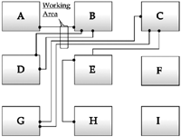
Figure 1 shows the general VLSI circuit with several high signal lines connected to it. In Figure 1, the crosstalk problem may occur in the working area due to the high density of the signal lines. High crosstalk in the working area can reduce the working ability of the VLSI circuit. The reduction of the crosstalk can improve the working ability of the VLSI circuit. In this section, research investigating some of the existing methods is considered [26], using them as a reference for other techniques in the next section.
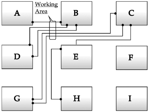
Figure 1 General Signal Line Connections in a VLSI Circuit.
3 Crosstalk-Reduction Techniques
Crosstalk is an unavoidable and usually unwanted capacitance. The capacitive effect will exist between the parts of electronic components. The parasitic factor of unwanted electromagnetic coupling from the source will be traced to the victim in the circuit. The coupling capacitance can be reduced by using various techniques.
3.1 Wire Spacing
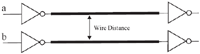
An important crosstalk factor is the distance between the lines as shown in Figure 2. The crosstalk, whether it has more or less intensity, must depend on the distance between the cables. The coupling capacitance will be increased or decreased depending on the distance between the cables. Therefore, the increasing distance between the cables can reduce crosstalk and this is one of the effective method’s advantage. This technique may affect the manufacturing cost via an increase in circuit area and production cost. When expanding the terming between adjacent wires, the coupling and whole loading capacitance can be significantly reduced. The power consumption and circuit timing will also be improved. Used space increasing will drastically reduce coupling capacitance. Coupling capacitance’s reduction can be directly converted into delay variation’s reduction due to crosstalk effects. However, wire spacing will be highly effective [27, 28].
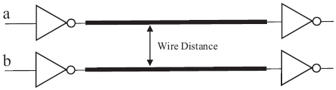
Figure 2 Wire Spacing between Two Buses.
3.2 Shielding
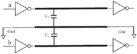
Popular crosstalk devaluation is the shielding insertion technique. This technique is used to reduce electromagnetic interference across channels. To reduce crosstalk efficiently, addition of a ground signal to the system is required. It will reduce the coupling capacitance (Cx) and the occurrence of skipping over signal channels. The ground track (Gnd) is a cable with no signal transition. This technique can be used to support the signal very well. Therefore, the ground tracks are considered to reduce the crosstalk noise by functioning as shields. Supply and insertion of the ground track between two data buses is possible by using a shielding technique [29]. The advantage of this technique is that it enables better delay prediction. This shielding is used for the long-distance buses that cross the entire chip. This technique is applied to controlling signal or global interconnects. The crosstalk-aware router can differentiate critical nets from others by utilizing low-frequency buses [30]. The router’s number and the capability of accessible segments are the same as the routing ability of the architecture limit of improvement [31, 32]. The ground insertion technique is shown in Figure 3.
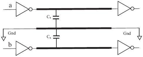
Figure 3 Ground Insertion between Two Buses.
3.3 Buffer Sizing
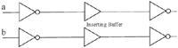
The buffer-sizing technique is one of the useful techniques for reducing crosstalk signals in transmission lines. The signal will interfere with the signal on the other line as shown in Figure 4. The buffer insertion technique is designed to reduce this problem by applying a buffer as a repeater. However, the length of the line is a major issue. If the number of threads per unit length was greater, then the signal interference in each cable will be distorted. This method is a good choice, if we want to reduce crosstalk signals in transmission lines. The cost of manufacturing and the complexity of the circuit design will be increased. This technique proposes to size up the switch buffers. The advantage of the buffer-sizing technique is in reducing the interconnect delay and crosstalk in the interconnect. The driving capacity is increased, and the transition is faster than ever. The associated problem in this method is the increased space and design complexity between the two groups. It needs extra spaces or some shields. The disadvantaged design of the buffer-sizing technique leads to increased power consumption and area cost [24].
3.4 Bus Encoding and Data Compression
Bus encoding and data compression are useful for reducing manufacturing costs. The advantage of the process is its ability to save space, store data, and use less network bandwidth by sending the compressed data. Moreover, the compressed data must be decompressed or decoded to get the original data back. There are two schemes of compressions: first, lossless data and second, compressed data without data loss. This technique is based on the frequency that contains duplicate data. The method helps to store the appeared position on the word. It can reduce the length of the collected data. The nature of data compression between lossless data and compressed data will be simultaneously recorded using the same information without distortion. The lossy data compression scheme has different concepts. The compressed data by using the principle of small data distortion is acceptable. For example, the human eye cannot completely distinguish certain colors; hence, there is no need to collect data of all colors. The advantage of partial data compression makes the data file size smaller but the data may have lost some details. Some form of data compression is often used with information systems to perceive the data. Timing is a critical issue in high-frequency systems [33]. This relies on the delay which is affected by the signal that must propagate through the physical length. Crosstalk, perioding between wires, and how long the multiple wires run in parallel to one another, with the quantity of crosstalk depended on the signal rise time, which also affects the signals on active wires switching simultaneously. Approaching bus encoding includes global data buses related code generation algorithm, developed to produce area-efficient crosstalk-avoidance (CA) codes [34]. The research has code memory to use overlapping boundaries [32, 35].
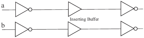
Figure 4 The Buffer Insertion Interconnect.
The shielding, buffer-sizing, and wire-spacing techniques can be used for mitigating the crosstalk problem in the VLSI circuit. The disadvantage of these techniques is that the size of the circuit might get extended. It can also lead to an increase in the price of the VLSI circuit. In the bus-encoding and data-compression technique, the size of the circuit will not be changed during the arrangement of the signal lines. Consequently, the price of the VLSI circuit will be stable.
4 Optimization Algorithms
In design optimization, the objective is to simply minimize the result. The cost of production could also be minimized. The efficiency of production will be maximized as well. An optimization algorithm is a procedure that is calculated iteratively by comparing solutions [36].
4.1 Genetic Algorithm
A genetic algorithm (GA) is an artificial intelligence technique, according to the theory of natural evolution by Charles Darwin. It inspires the GA as a search heuristic. This algorithm is used in searching for increasing efficiency and learning. The theory of natural evolution of GAs has many advantages of being resistant from errors for finding the complex answers and difficult data sources. This search process is not included in the particular model or any type of data. Holland [33] proposed that Darwin’s theory is based on the GAs. The GA is one of the widely used algorithms to solve scientific and engineering problems.
4.2 Memetic Algorithm
The memetic process is a hybrid process of the GA and local search. The algorithm uses the basis of the memetics theory of Dawkins. This algorithm represents the solution to find the answer in function. There are some steps, which are similar to the GA, e.g., the random method is replaced with a chromosome. Then the pattern will be switched between the chromosome parent (crossover) and mutation. The mutation creates a new answer. Searching for a specific area might be used in the clustering methods of nearby nodes to develop the poorest answers in the group and to maintain fine results. This step depends on the local search techniques. Memetic algorithms were developed by Merz and Freisleben [37]. This method is similar to the GAs; however, memetic algorithms can also be used in a local search by using a meme gene in the chromosome.
4.3 Particle Swarm Optimization
Particle swarm optimization is a method for finding random answers (random search algorithm). This is one of the methods of the GA, and is applied to solve engineering problems. This method is another way to find the best answer and value without using an unconstrained problem. This algorithm is used for finding the answer and making the value of the function. The objective function of the best value depends on the highest or the smallest value. Particle swarm optimization was proposed by Kennedy and Eberhart [38]. This method was inspired by observing the flying behavior of birds, which swarm while looking for food in the most suitable place.
4.4 Ant-Colony Optimization
Ant colony optimization (ACO) is the high-efficiency heuristic method in the swarm intelligence group. It consists of many single units and goals. Each unit can exchange information for operations in the local area. The information will be transferred to create a route step and set of answers. This technique can make every unit achieve the target. The basic principle of the ACO comes from finding food by the ant colony and then creating a route to transport the food back to the nest. To find food, many ants will leave the nest and bring a portion of food back to the nest. They leave the pheromone on the ground. Pheromones can evaporate over time. This pheromone trail is a path for other ants to carry their food from the food source. The first ant returning with food will get the shortcut path to the food source. The number of pheromones left along the path will be increased steadily with the amount of food quality. The approaching path is used to find the best available path. This increase in pheromones is an important update of each route. The quantity and quality of food decrease slowly with reducing pheromone concentrations. The ants will begin to search for new food sources. Dorigo and Birattari [39] developed the ACO. Thus, this is a method that is inspired by observing the shortest distance for food transportation by ants.
4.5 Shuffled Frog-Leaping Algorithm
The shuffled frog-leaping algorithm (SFLA) technique is a method that uses the strength of frogs. This is similar to the GA method, in that it is used to select a species or chromosome to survive, and hence eliminate the bad chromosome. The SFLA procedure starts with determining the number of frogs and determining the strength of each frog. The strength of each frog is graded from high to low. The pattern is divided into a group of frogs, and further into subgroups. There are called memeplexes. Each memeplex contains the duplex. It will allocate the number of frogs. The sum of frogs is contained in the memeplex. It equals the number of allocated frogs at the beginning. The strength of the frogs will be determined to evaluate each frog. This order will help to choose the frog with the least strength. The weakest result is used to get rid of the weakest frog from the memeplex. This process will be repeated until the specified calculation cycle is completed. The SFLA approach was proposed by Eusuff and Lansey [40]. This method is similar to the selection of the strongest frog. Groups of frogs are separated in the memeplex for searching a portion of food in the local area. The searched results will be exchanged for every frog in the memeplex. The worst and best frogs, Cb, and Cw, will be identified. The best frog in all the memeplexes will be called the global best frog (Cg).
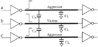
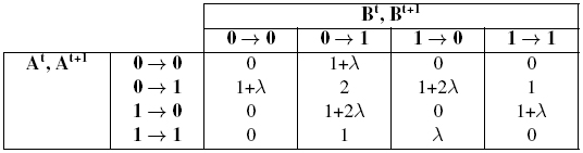
This research proposes a novel method for developing crosstalk minimization. It aims to reach total energy minimization effect Attempts to decrease the total energy capacitance in optimization would require rearranging the wire’s signal transition. This can be set in each activity from the data’s bus wires. The proposed method considers signal integrity and allows power reduction at the same time; however, it obtains the most effective arrangement of the signal. An optimization model is needed for this technique. Crosstalk is a major, limiting factor in the VLSI design. High coupling capacitance between wires represents a major effect due to capacitance. In the VLSI design, constraining coupling capacitance (Cx) will exceed the capacitance between the lines (self-capacitance, CL) and the transition ground. Figure 2 reveals the electrical equals to a primary three-wire bus, where the two outer lines (a and c) present a rising transformation. Line b exhibits a decreasing transformation. It will assume the total bus driver will clock. Lines a and c (the aggressors) can affect the transformation on b (the victim) to turn it into a non-ideal entity. The effects of the huge coupling capacitance between c and b will be as follows: (i) delaying the transformation on b and (ii) affecting an initial negative spike at b [41].
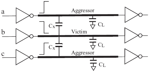
Figure 5 Crosstalk on a Three-Line Bus.
Table 1 Normalized Energy on Two Adjacent Busses [31]
In this study, a wide-spaced wire has the advantages of both power and delay, but it affects the cost in the area [41]. Our assumption has included some minimal area between guaranteed wires. All the signal integrity and timing requirements will be appropriated. A rule of new minimal area is essential to achiev the rule of technical design. The design concept is considered as an adjacent bus. We firstly need a power model to assess the best line area, i.e., spacing through energy.
The energy form per cycle (Ebus) for a bus wire (measured in joules, in SI) will include two capacitive effects [31]:
| (1) |
where Vdd is the voltage across the capacitor, αX and αL represent the rates at each switching capacitance, αL signify the fundamental lines switching activity, and αX represents the simultaneous transformation of two adjacent lines when lines a and b are changed in time. Further, CL is load capacitance in the buses. These are only two transformation pairs that cause CX to switch: (i) when both a and b change differently into final values and (ii) when the first two lines switches, the other will not change, and their final values are not similar. The average energy consumed by a line with clock frequency f = (1/Tclk) can be
| (2) |
where n represents the clock cycles and Ic(t) is the drawn current because of transformation in a clock period. Qav is the generated time-averaged charge to be provided to all interconnect capacitances. The SFLA can search the optimal pattern in the layout easily, identifying the different generations and sequences of a result of the VLSI channel. Figure 6 provide a detailed description of the design algorithm [42]. The process of crosstalk reduction in the VLSI circuit, used in this study, is also shown in Figure 6.
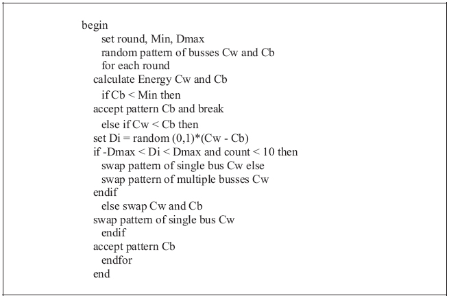
Figure 6 Crosstalk Reduction with SFLA.
The process begins with the determination of the chromosome. This step can be done with the solution. Each chromosome is comparable to the solution group. The result is changed by using the crossover methods and mutation. This step refers to the GA. In the process, there are symbiotic methods. The local finds help to improve the population’s efficiency. For a better solution, the results will be evaluated for fitness evaluation values to chromosome selection. The results represent the population of the next generations. The process is explained as follows.
First, chromosome representation constitutes the coding of the problem. The construction of a list in obligation units can be represented by numbers. Second, population initialization is a sampling of genetic components. There are many chromosomes, which represent the correct answer or answer pattern. The chromosome number may be randomly generated by the size of the population. Third, genetic operations consist of swapping species and mutation by selecting the parent chromosome from the population to create a child chromosome. The species is randomly selected by the parent chromosome. They come to capture the cut and/or alternate styles from the chromosome parent to get the child chromosome. The number of the parent chromosome will be chosen at random according to the probability value of swapping constraints. The new set of chromosomes is the number of primary chromosomes that will be selected. According to the probability, the mutation is a random selection of the original chromosome. Fourth, the local search is often used in the genetic movement with the hope of increasing the effectiveness of the methodology. This study applies a specific search to the area. Fifth, fitness evaluates the decoding chromosome. The calculations of the suitability value, which is according to the target function, are referred to the appropriated function of problems. It represents the suitability of each chromosome. They will be used to determine the probability of existence to survive. Finally, chromosome selection is used to calculate the next generation population. The selection process is the process of the number of sampling times. The sampling factor is equal to the size of the population. If the sampling fails in any chromosome, it will be demoted to the next generation. This process will repeat forward until it meets the termination criterion. The SFLA is used for rearranging the buses to minimize the total crosstalk energy. In the memeplex, the best and worst frogs are labeled as Cb and Cw, respectively, and the best frog in all the memeplexes is called the global best frog (Cg). In every round of the searching process, the worst frog (Cw) will first be developed by changing the searching position (Di) of the frog, as shown in the following equations:
| (3) |
| (4) |
To improve the suitable position of the worst frog, the number of searching rounds will be specified. In this study, the SFLA is used to optimize the suitable arrangement of the signal lines in the VLSI circuit; this is because the optimal time obtained in this method is the shortest time when compared with the other mentioned methods.
5 Results and Discussion
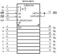
For the optimization study, we rearranged the buses between boxes A and B, specified as SN74ALS867A (fully programmable with synchronous counting and loading). These synchronous 8-bit up/down counters feature internal carry and presentable look-ahead circuitry for cascading in high speed counting applications. Two counts enable inputs with a count rate of 35 MHz. This is an asynchronous master reset (clear). The clock and all other control inputs are dependent on the input. All other control inputs of the overrides are active only during the rising clock edge state.
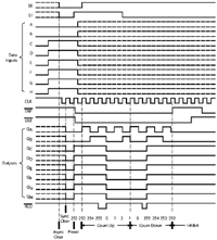
The timing diagram is shown in Figure 8. The connection between boxes A and B using the IC SN74ALS867A for testing crosstalk reduction is presented in Figure 7. The experimental results showed that Cx can be up to three times larger than CL [43] and Cx = CL (for 0.25 μm technology). The effects of crosstalk on buses were being quantified by the objective; the structure depicted has been simulated by us. The example circuit in Figure 5 has all 22 signal lines, consisting of control and data lines. If all the case searches were performed, the layout would comprise 22! patterns. This case is an example of a hard problem that takes a lot of search time. When the SFLA is applied to the search, the results appear in the conclusion. This method is used to decrease the searching time. Compared with other algorithms [5], the SFLA works effectively with the adjustment of Dmax, Min value, and the number of appropriate cycles. The experimental results are shown hereunder.
From Table 2, we set the values of Dmax =100 and Min = 100, with the total crosstalk energy in the optimal pattern of 5690. At around 856,443,278 from 1,000,000,000 cycles, we obtain the lowest crosstalk pattern that targets the total energy minimization effects with the programming process. The average total energy was equal to 6545.33, but the original pattern (original) had total energy equal to 8950. We reduced the total energy through capacitance by rearranging the wires’ signal transition. The result of the optimal pattern is 36.42% lower than the cost of the original result and 13.06% lower than the cost of the average value. When we compared the SFLA with the simulated annealing (SA) algorithm, we found that the SFLA was able to find the optimal pattern in 1,000,000,000 iterations and the SA also was able to find the optimal pattern in 1,500,000,000 iterations. The result shows that SFLA is more efficient than the SA. This is important particularly when calculating in high-complexity circuits.
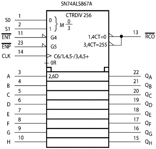
Figure 7 Data Layout of SN74ALS867A.
In this section, the SFLA algorithm is employed to solve many problems. The different populations of study cases were used to evaluate the proposed technique. According to the self-adaptive rule it is better to conclude the result of the parameters and compare the same with the ACO algorithm. Table 3 shows the hypothesis results of the various population numbers of the SFLA and ACO. The results are not sensitive to the individual population number. Table 3 also shows that the effective run time is less than the other algorithm. In the experiments, the building data set has many different patterns of clock cycles and task execution times. The schedulable pattern of the data set of control and data bus is also displayed. The ACO algorithm is more time consuming than the SFLA algorithm. The SFLA algorithms can acquire a feasible solution of almost less than 30–50% in all the conditions.
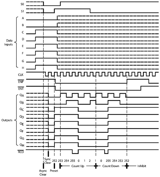
Figure 8 Timing Diagram of SN74ALS867A.
Table 2 The Results of SFL Optimization
| Iteration | Optimized Value |
| 10,00,000 | 6,180 |
| 50,000,000 | 5,920 |
| 100,000 000 | 5,730 |
| 500,000,000 | 5,710 |
| 1,000,000,000 | 5,690 |
| 2,000,000,000 | 5,690 |
Table 3 The Running Time with Different Testing Number between SFLA and ACO Algorithm
| Testing number | ACO (ms) | SFLA (ms) |
| 10 | 22.43 | 15.67 |
| 20 | 39.37 | 17.84 |
| 30 | 72.50 | 37.43 |
| 40 | 112.84 | 39.27 |
| 50 | 312.74 | 198.66 |
| 60 | 950.88 | 464.87 |
| 75 | 1297.31 | 752.99 |
| 90 | 2439.49 | 1234.26 |
| 100 | 4683.98 | 2286.27 |
| 125 | 5227.73 | 2831.63 |
| 150 | 7238.08 | 3673.56 |
6 Conclusion
This paper is included with an experiment with results indicating various trends in the elevations and further growth of the VLSI design. Most of the electronic circuits are based on the VLSI design, according to its appropriate size, more self-sufficiency, less power consumption, and proper range of operations. This study examined the wiring path signal with disturbance using the theory of optimization, which helps in the search for a model to the most profitable sort of the signal lines with signal transition consideration. The method using the SFLA algorithm is used to optimize for the most accurate value in the arranged signal lines that will result in minimal noise. Therefore, this paper has examined, based on the crosstalk noise reduction experiment in the VLSI design and the SFLA, and found that the method can be used for finding the profitable array pattern. The search time for finding a profitable solution was significantly decreased when compared with other algorithms. The SFLA worked best depending on the parameters selected; however, multiple objectives should be applied in the future for further testing. Furthermore, the optimization of the VLSI design with several algorithms has been calculated. Moreover, the particular performance measures have also been estimated to solve the profitable values precisely. Finally, the research objectives and further directions are presented through this experiment.
References
[1] R. K. Pal, ‘Multi-Layer Channel Routing Complexity and Algorithms’ Boca Raton: CRC Press, 2000.
[2] W. Wolf, ‘Logic gates: logic, circuits’, In Modern VLSI design: system-on-chip design, Upper Saddle River, NJ: Prentice Hall, pp. 169–172, 2002.
[3] S. Saini and S. B. Mandalika, ‘A new bus coding technique to minimize crosstalk in VLSI bus’, In The 2011 3rd international conference on electronics computer technology, 2011.
[4] E. Afzalan, M. A. Taghikhani, and M. Sedighizadeh, ‘Optimal placement and sizing of DG in radial distribution networks using SFLA’, International Journal of Energy Engineering, vol. 2, no. 3, pp. 73–77, 2012.
[5] W. Wongthatsanekorn, ‘Reviewing and comparisons of five evolutionary-based algorithms’, The Journal of KMUTNB, vol.19, no.2, pp. 285–290, 2009.
[6] A. Terapasirdsin and N. Wattanapongsakorn, ‘Crosstalk aware global router in VLSI design’. In The 6th international joint conference on computer science and software engineering (JCSSE 2009), 2009.
[7] V. P. Saxena and C. L. Liu, ‘A post processing algorithm for crosstalk-driven wire perturbation’, IEEE Transactions on Computer-Aided Design of Integrated Circuits and Systems, vol. 19, no. 6, pp. 691–702, 2000.
[8] N. Hanchate and N. Ranganathan, ‘A linear time algorithm for wire sizing with simultaneous optimization of interconnect delay and crosstalk noise’, In 19th international conference on vlsi design held jointly with 5th international conference on embedded systems design (VLSID’06), Hyderabad, India, 2006.
[9] N. Hanchate and N. Ranganathan, ‘Simultaneous interconnect delay and crosstalk noise optimization through gate sizing using game theory’, IEEE Transactions on Computers, vol. 55, no. 8, pp. 1011–1023, 2006.
[10] I. H.-R. Jiang and Y.-W. Chang and J. Y. Jou, ‘Crosstalk-driven interconnect optimization by simultaneous gate and wire sizing,’ IEEE Transactions on Computer-Aided Design of Integrated Circuits and Systems, vol. 19, no. 9, pp. 999–1010, 2000.
[11] S. Thakur, K. Y. Chao and D. F. Wong, ‘An optimal layer assignment algorithm for minimizing crosstalk for three-layer VHV channel routing,’ In Proceedings of ISCAS’95 - international symposium on circuits and systems, seattle, pp. 207–210 vol.1., 1995.
[12] H. Kaul, D. Sylvester, and D. Blaauw, ‘Performance optimization of critical nets through active shielding’, IEEE Transactions on Circuits and Systems I: Regular Papers, vol. 51, no. 12, pp. 2417–2435, 2004.
[13] S. Singh and V. SulochanaVerma, ‘Reduction of crosstalk noise and delay in VLSI interconnects using schmitt trigger as a buffer and wire sizing’. In Meghanathan N., Nagamalai D., Chaki N. (eds), ‘Advances in computing and information technology’, Advances in Intelligent Systems and Computing, vol 178. Springer, Berlin, Heidelberg, 2013.
[14] P. Chen, D. A. Kirkpatrick and K. Keutzer, ‘Miller factor for gate level coupling delay calculation’, In IEEE/ACM International Conference on Computer Aided Design. ICCAD - 2000. IEEE/ACM Digest of Technical Papers, pp. 68–74, 2000.
[15] S. Ramprasad, N. R. Shanbhagand, and I. N. Hajj, ‘Analytical estimation of signal transition activity from word-level statistics’, IEEE Transactions on Computer-Aided Design of Integrated Circuits and Systems, vol. 16, no. 7, pp. 718–733, 1997.
[16] S. Gupta and S. Katkoori, ‘Intrabus crosstalk estimation using word-level statistics’, IEEE Transactions on Computer-Aided Design of Integrated Circuits and Systems, vol. 24, no. 3, pp. 469–478, 2005.
[17] S. Gupta, S. Katkoori and S. Sankaran, “Floorplan-based crosstalk estimation for macrocell- based designs’, In 18th international conference on VLSI design held jointly with 4th international conference on embedded systems design, pp. 463–468, 2005.
[18] C. G. Lyuh, T. Kim, and K. W. Kim, ‘Coupling-aware high-level interconnect synthesis [IC layout]’, IEEE Transactions on Computer-Aided Design of Integrated Circuits and Systems, vol. 23, no. 1, pp. 157–164, 2004.
[19] P. Kollig and B. M. Al-Hashimi, ‘Simultaneous scheduling, allocation, and binding in high level synthesis’, Electronics Letters, vol. 33, no. 18, pp. 1516–1518, 1997.
[20] R. J. Cloutier and D. E. Thomas, ‘The combination of scheduling, allocation, and mapping in a single algorithm’, In 27th ACM/IEEE Design Automation Conference, pp. 71–76, 1990.
[21] H. Sankaran and S. Katkoori, ‘Floorplan driven high level synthesis for crosstalk noise minimization in macro-cell based designs’, In 2009 IEEE Computer Society Annual Symposium on VLSI, pp. 274–279, 2009.
[22] H. Sankaran and S. Katkoori, ‘Simultaneous scheduling, allocation, binding, re-ordering, and encoding for crosstalk pattern minimization during high-level synthesis’, IEEE Transactions on Very Large Scale Integration (VLSI) Systems, pp. 217–226, 2011.
[23] H. Sankaran, ‘High-Level Synthesis Framework for Crosstalk Minimization in VLSI ASICs’, University of South Florida, 2008.
[24] M. Lampropoulos, B. M. Al-Hashimi, and P. Rosinger, ‘Minimization of crosstalk noise, delay and power using a modified bus invert technique’, In The proceedings design, automation and test in Europe conference and exhibition, 2004.
[25] K. N. Patel and I. L. Markov, ‘Error-correction and crosstalk avoidance in DSM busses’, IEEE Transactions on Very Large Scale Integration (VLSI) Systems, vol.12, no.10, pp. 1076–1080, 2004.
[26] A. Terapasirdsin and N. Wattanapongsakorn, ‘Row-based design for wiring length and crosstalk minimization in ULSI chip’, In The 2nd international conference on electrical engineering/electronics, computer, telecommunications and information technology (ECTI-CON 2005), 2005.
[27] H. Schmit and V. Chandra, ‘FPGA switch block layout and evaluation’, In The proceedings of the 2002 ACM/SIGDA 10th international symposium on field-programmable gate arrays, 2002.
[28] C. Kuang-Chin and J. Jing-Yang, ‘A code generation algorithm of crosstalk-avoidance code with memory for low-power on-chip bus’, In The 2008 IEEE international symposium on VLSI design, automation and test (VLSI-DAT), 2008.
[29] A. B. Kahng, S. Muddu, E. Sarto and R. Sharma, ‘Interconnect tuning strategies for high-performance ICs’, In The proceedings design, automation and test in Europe, 1998.
[30] S. J. E. Wilton, ‘A crosstalk-aware timing-driven router for FPGAs’, In The proceedings of the 2001 ACM/SIGDA ninth international symposium on field programmable gate arrays, 2001.
[31] Z. Junmou and E. G. Friedman, ‘Crosstalk noise model for shielded interconnects in VLSI-based circuits’, In The IEEE international [systems-on-chip] SOC conference, 2003.
[32] N. A. Sherwani, ‘Design and fabrication of VLSI devices’, In Algorithms for VLSI physical design automation’, New York: Springer US, pp. 39-74, 1999.
[33] J. H. Holland, ‘Adaptation in natural and artificial systems: an introductory analysis with applications to biology, control, and artificial intelligence’, Cambridge, MA: MIT Press, 1992.
[34] D. Chunjie, Z. Chengyu and S. P. Khatri, ‘Forbidden transition free crosstalk avoidance CODEC design’, In The 2008 45th ACM/IEEE design automation conference, 2008.
[35] L. Macchiarulo, E. Macii and, M. Poncino, ‘Wire placement for crosstalk energy minimization in address buses’, In The Proceedings 2002 Design, Automation and Test in Europe Conference and Exhibition, 2002.
[36] W. W. Hines, D. C. Montgomery, D. M. Goldsman and C. M. Borror, ‘Finite sample spaces and enumeration: permutations, combinations’, In Probability and statistics in engineering, Hoboken, N.J.: John Wiley & Sons, pp. 15–16, 2003.
[37] P. Merz and B. Freisleben, ‘A genetic local search approach to the quadratic assignment problem’, In The proceedings of the 7th international conference on genetic algorithms, 1997.
[38] J. Kennedy and R. Eberhart, ‘Particle swarm optimization’, In The proceedings of ICNN’95 - international conference on neural networks, 1995.
[39] M. Dorigo, V. Maniezzo and A. Colorni, ‘Ant system: optimization by a colony of cooperating agents’, IEEE Transactions on Systems, Man, and Cybernetics, Part B (Cybernetics), vol. 26, no.1, pp. 29–41, 1996
[40] M. M. Eusuff and K. E. Lansey, ‘Optimization of water distribution network design using the shuffled frog leaping algorithm’, Journal of Water Resources Planning and Management, vol.129, no.3, pp. 210–225, 2003.
[41] P. Sotiriadis and A. Chandrakasan, ‘Bus energy minimization by transition pattern coding (TPC) in deep submicron technologies’, In The proceedings of the 2000 IEEE/ACM international conference on computer-aided design, 2000.
[42] J. William Paul Swartz, ‘Automatic layout of analog and digital mixed macro/standard cell integrated circuits’, Yale University, 1993.
[43] D. Jariwala and J. Lillis, ‘On interactions between routing and detailed placement’, In The IEEE/ACM international conference on computer aided design, ICCAD-2004, 2004.
Biographies
Apichat Terapasirdsin received his B.S. degree in electronics engineering (second class honors) in 1997 and the M.Eng. degree in computer engineering in 2000, both from the King Mongkut’s University of Technology Thonburi (KMUTT), Bangkok, Thailand. He was an affiliated student at the Department of Computer Science, the State University of New York at Binghamton (SUNY), USA, in 2008. He is currently a Ph.D. student in IT Management, Faculty of Engineering, Mahidol University, Thailand. His areas of research interest are optimization of VLSI design and computer architecture.

Supaporn Kiattisin received her B.Eng. degree in applied computer engineering from the Chiang Mai University, Chiang Mai, Thailand, in 1995, and the M.Eng. degree in electrical engineering and the Ph.D. degree in electrical and computer engineering from the King Mongkut’s University of Technology Thonburi, Bangkok, Thailand, in 1998 and 2006, respectively. She is currently the program director of Information Technology Management, Faculty of Engineering, Mahidol University, Thailand. Her research interests include computer vision, image processing, robot vision, signal processing, pattern recognition, artificial intelligence, IoT, IT management, digital technologies, big data, and enterprise architecture with TOGAF 9 certification. She is a member of the IEICE and TESA. She served as the Head of IEEE Thailand Chapter in Biomedical Engineering. She also served as the Chairman of the TimesSOC Transaction Thailand. She has expertise in enterprise architecture (EA), data sciences, information technology in E-government, and digital economy (DE).
Journal of Mobile Multimedia, Vol. 16_1-2, 221–244.
doi: 10.13052/jmm1550-4646.161211
© 2020 River Publishers