High Sensitivity Non-split Drain MAGFET for Wireless Sensor Networks
Rattapong Nakachai1, Amporn Poyai2, and Toempong Phetchakul1,*
1Department of Electronics, Faculty of Engineering, King Mongkut’s Institute of Technology Ladkrabang, Bangkok, Thailand
2Thai Microelectronics Center, Design & Engineering Consulting Service Center (DECC), National Science and Technology Development Agency (NSTDA), Thailand
E-mail: R.nakachai@gmail.com; Amporn.poyai@nectec.or.th; Toempong.ph@kmitl.ac.th
* Corresponding Author
Received 30 April 2020; Accepted 17 May 2020; Publication 17 August 2020
Abstract
The non-split drain MAGFET proposed in this paper is aspossess an ideal, highest sensitivity in the same type of device, current mode for low power, and low voltage that can be embedded within a system for wireless sensor networks application. It is a split-drain MAGFET that is designed to have no gap between drains so that there is no loss from the gap. There are two split contacts in one drain to represent the split drains for current difference that induced from due to magnetic field. The relative sensitivity comparison among all the gaps (3, 2, 1, and 0 μm) with all aspect ratio of width (W)/length (L) (L/W = 1, 0.6, and 0.2) at biased current 0.25 mA shows that the zero gap or the non-split drain MAGFET structure gives the highest sensitivity. The sensitivities of the non-split drain at the aspect ratios L/W = 1, 0.6, and 0.2 in this study are 0.0595, 0.0479, and 0.0231 T−1, respectively. It is proved that the gap is not necessary for the MAGFET. It is a new, smart way to design the MAGFET for the highest sensitivity and gap lossless for modern sensor applications.
Keywords: Non-split drain, MAGFET, TCAD, magnetic sensor, Lorentz’s force.
1 Introduction
Future trends of increasing the efficiency of magnetic field detectors will focus on continuously improving to a smaller size, low power consumption, and high sensitivity, suitable for application in various environments [1]. Nowadays, there is a proposal to apply magnetic sensors to check the position of the vehicle, including, developing algorithms as wireless magnetic sensor networks for real-time traffic flow monitoring and data processing for a road network [2–4]. For smart systems, the sensor can be integrated within the processor chip which as all of them are work efficiently even in low voltage and low power operation. The sensor device should be in current mode for signal processing. The small size of them needs requires the a high high-performance device such as a device that is capable of the reducing the subthreshold swing in MOSFET for increasing the ON state current/OFF state current ratio of for the gain of the device.
The spilt-drain MAGFET is a kind of magnetic sensor that detects the vertical magnetic field perpendicular to drain current [5]. It is the MOSFET that is specially designed by the split drain into two symmetry symmetrical parts D1 and D2 for receiving current difference from Lorentz’s force that linearly depends on magnitude and direction of vertical magnetic field density [6]. The MAGFET is a low power device compatible to with modern CMOS technology for low power and low voltage integrated circuit [7–9].
This study introduces a new design of the MAGFET for high sensitivity. The split-drain MAGFET generally should be designed such that the gap between drains would be kept as a minimum value as possible as we can for realizing high sensitivity. This activity depends directly on fabrication technologies. The non-split drain MAGFET has no gap between split drains but there are still split contacts into a single drain for differential output current according to magnitude and direction of the vertical magnetic field. This new design has no gap; so, it does not depend on fabrication technologies and hence proves that gap is not necessary. This design will give the highest sensitivity and approach to the ideal condition with the lossless from the gap.
2 Hall Effect: Mode of Operation
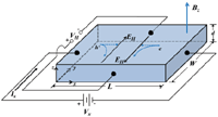
Hall effect is the basic basis of for nonferromagnetic material for magnetic devices. This effect is indicates that there is an induced force on a moving charge particle q in the magnetic field. Figure 1 illustrates this the Hall effect of a semiconductor that whose carriers are hole and electron. The force that is called the Lorentz’s force is given by
| (1) |
where F is the induced force vector, q is the particle charge, v is the drift velocity, and B is the magnetic field density vector. Electrons and holes flowing in a material by Ix will experience a force in −y direction as indicated in Figure 1. The electric field EH or the Hall field is induced for balancing the force and may be written as
| (2) |
The Hall field gives the Hall voltage between the top and bottom sides of the material which is
| (3) |
for a p-type semiconductor or majority hole carrier material and
| (4) |
for an n-type semiconductor or majority electron carrier material as shown in Figure 1.
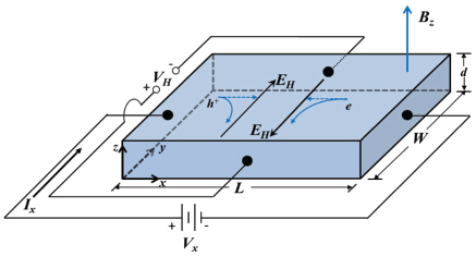
Figure 1 Geometry and structure of hall effect.
There are two modes of operation of the Hall effect for magnetic sensors that enables classification of devices into two groups. The first group uses the regular Hall effect structure as shown in Figure 1 in which the length L is longer than the width W. The output is the Hall voltage which is related to magnitude and direction of the magnetic field. The second group uses the Lorentz’s force and the output is differential current or magnetoresistance. In this group, since the Lorentz’s force is preferred, there is no need for the Hall field to balance with the Lorentz’s force. The structure needs to be designed in such a way that it is different from the voltage mode group in which the length L is shorter than the width W. The two modes of operation are applied for magnetic devices such as the Hall plate, vertical Hall in voltage mode and magnetoresistance, magnetotransistor, and the MAGFET in current mode.
Voltage mode
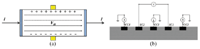
The concept of the voltage mode Hall effect device is shown in Figure 1. The Hall voltage will be induced by the magnetic field according to (3) and (4) for the p-type and n-type, respectively. In this mode, the electric force from the Hall field balances the Lorentz’s force so the total force is zero and the Hall voltage appears between the top and bottom sides of the device. The Hall device has four terminals: two for current and two in vertical for the Hall voltage sensing. Figure 2(a) shows the top view of the Hall plate devices. The current paths are straight even though the Lorentz’s force acts upon the carrier but the Hall electric field balances this force. The Hall plate is very popular useful for the magnetic sensor in the voltage mode for vertical field detection. It can detect both magnitude and direction of the magnetic field. There is another Hall device that detects the horizontal magnetic field. Figure 2(b) is the vertical Hall plate device that detects the horizontal or parallel field. There are 5 five contacts for three current contacts and the two Hall voltage contacts. The main mechanism still uses the Hall effect in vertical direction.
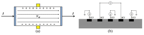
Figure 2 Hall effect voltage mode of operation: (a) Hall plate device and (b) Vertical hall device.
Current mode
The current mode Hall device uses the Lorentz’s force for deflecting carrier current. This mode does not want require the Hall electrical field for balancing the Lorentz’s force. The device has to be designed as a short structure. The length L in Figure 1 is shorter than the width W for reducing the induced Hall electrical field as much as it can. The Lorentz’s force deflects the carrier in current as shown in Figure 3. The total force F can be written as
| (5) |
for hole and electron, whereas vp and vn are drift velocity of hole and electron, respectively. The hole and electron current density Jp(B) and Jn(B) in the presence of a magnetic induction B can be written as
| (6) |
where μp and μn are hole and electron mobility, respectively. Jp(0) and Jn(0) are the drift current densities due to the electric field E, Vx/L, when B = 0:
| (7) |
where p and n are hole and electron concentration, respectively.
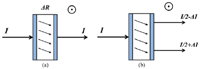
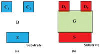
The orientation of vectors E and B correspond to those in Figure 1. From the current densities vector in (7), the Hall current mode of the operational device can be applied in current deflection and magnetoresistance path as shown in Figure 3. The deflection current paths are longer than regular path of no magnetic field, and that also means greater effective resistance of the material. The magnetoresistance device has two terminals and resistance increases with magnetic field. This magnetoresistance effect is caused by design Hall plate in short structure, so it is called geometry magnetoresistance which is shown in Figure 3(a). Another type of current mode device is shown in Figure 3(b). This device is designed for three terminals. The currents flow in one terminal, pass through the device, and flow out equally to the other two terminals. The current deflection by applied magnetic field will make a difference in terms of the output current. One side has to design split contact symmetrically for carrying differential current corresponding to the magnetic field density. The current mode split terminal devices, for example, are the magnetotransistor and the MAGFET. These devices have to be designed for receiving current region, collector for the magnetotransistor, and drain for the MAGFET, in two split symmetrical regions or terminals. Figure 4 shows a top view of the magnetotransistor and MAGFET. The collector is split into two collectors as C1 and C2 and the drain is split into two drains as D1 and D2 as shown in Figure 4(a) and 4(b), respectively. These devices use this design from the first time that they were introduced. Even though they were continuously developed along in the recent past time but the design concept is never changed. It is well known that the MAGFET has another name that we call split drain MOSFET because the structure is designed to split the drain into two symmetrical regions.
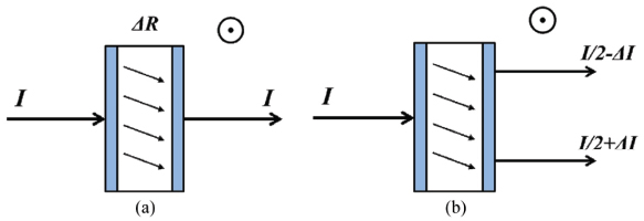
Figure 3 Current mode hall effect: (a) Magnetoresistance and (b) Current deflection.

Figure 4 Current mode hall effect devices: (a) Magnetotransistor and (b) Split-drain MAGFET.
The point of these current mode devices is a gap between the split regions. It is believed that the split region is necessary for the current mode devices. It is well known that the gap causes some loss in the differential current output from the ideal device. These devices are recommended to keep this gap small as possible as they can. Unfortunately, the minimum gap depends on fabrication technologies. In this study, the new design concept is proposed and proved that a gap is not necessary for the current mode device. The gap causes the nonuniform current distribution and current deflection in this area. The real point is that the contact current is the most important parameter for carrying the differential output current but do not separate the drain region. It will make one to contemplate changing design ideas. Our proposed design is smart, easy, and independent from any technological limitation. This design will also apply to other current mode Hall effect devices.
3 Device Structures and TCAD
3.1 Device Structure
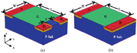
The device structures of the conventional MAGFET and non-split drain MAGFET are shown in Figures 5(a) and (b), respectively. The conventional split-drain MAGFET is the MOSFET that has two split drains with the gap (d) between them. The non-split drain is the conventional MAGFET that has no gap. The channel length (L) and width (W) are shown in Figure 5. The gaps are varied at 3, 2, 1, and 0 μm. The aspect ratios (L/W) with the minimum distance of 1 μm are varied at 0.2, 0.6, and 1. The substrate is the n-type silicon with the concentration of 1015 cm−3. The n-type concentration of source and drain are is 1018 cm−3 and SiO2 as gate insulator has a thickness of 500 Å. There are two contacts in two split drains for the conventional MAGFET and when gap is zero in Figure 5(b), there are the same two contacts in one drain.
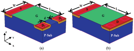
Figure 5 Device structure: (a) Conventional MAGFET and (b) Non-split drain MAGFET.
3.2 TCAD
TCAD sentaurus is the a standard process and device simulation program [10–13]. It is used as a tool for this study. There are important equations such as Fermi-Dirac probability, incomplete ionization of dopants, drift and diffusion current, current continuity equation, and Poisson equation. They are solved simultaneously with few or no approximation. The model for the magnetic effect is as follows
| (8) |
where ∝ is the n- or p-type semiconductor, J∝ is the carrier current density vector, g∝ is the current vector without mobility, is the the Hall mobility, B is the magnetic induction vector, and B is the magnitude of vector [14].
4 Results and Discussion
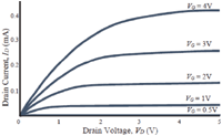
The current–voltage characteristics of devices in Figure 5 are measured to confirm that they operate as the MOSFET. Two drains are connected together as one drain during the measurement. The current–voltage characteristic of the device, L/W = 1, is shown in Figure 6. It shows good characteristics with the threshold voltage, VT, approximately 0.5 V. The saturation current is a function with (VG − VT)2, which is according toin accordance with the regular long channel MOSFET.
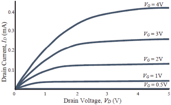
Figure 6 Current-voltage characteristics of MAGFET.
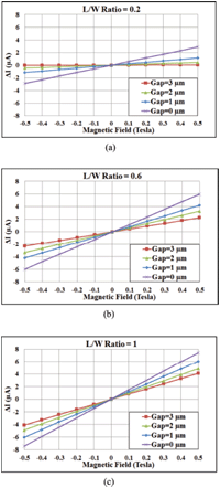
Figure 7 shows magnetic responses of all the devices. The constant current source pulls the current down from source to ground. The biased current is controlled by constant current source to avoid output differential current from the magnetic field modulation. Normally ID 1 and ID2 are equal except that there are some offset values from the fabrication process when there is no magnetic field. The total drain currents ID are the sum of drain 1 and drain 2 currents, (ID1 + ID2), which is according toas per the constant current source. The output responses are current difference (ΔID = ID1 − ID2) causes caused by the Lorentz’s force according to magnitude and direction of the vertical magnetic field. Figures 7(a) to 7(c) show responses of the devices aspect ratios as 0.2, 0.6, and 1, respectively. The gaps are varied at 3, 2, 1, and 0 μm in each device. All of the characteristics (ΔI − B) show linearly dependence.
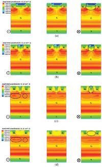
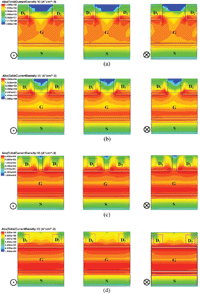
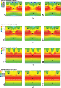
Figure 7 shows the ΔI − B magnetic responses of the MAGFET. The magnetic fields varied varying from −0.5 to 0.5 T are applied in a vertical perpendicular direction to a planar device. The relation between output differential current ΔI and magnetic field density B is linear. The voltage source VD at drain and VG at gate is 1 V and constant current source is 0.25 mA. The relative sensitivity sensitivities (Sr = ΔI/ΔB.I) of L/W = 0.2 with gaps at 3, 2, 1, and 0 μm are 0.0003, 0.0036, 0.0092, and 0.0231 T−1, respectively. The magnetic responses of the aspect ratio L/W = 0.6 are shown in Figure 7(b) in the same condition. The relative sensitivities, Sr are 0.0182, 0.0264, 0.0338, and 0.0479 T−1, respectively. Similarly, the magnetic responses of the aspect ratio L/W = 1 are shown in Figure 7(c) and the relative sensitivities Sr are 0.0326, 0.0389, 0.0481, and 0.0595 T−1, respectively. It is seen that the higher the sensitivity, the less the gap it is. All of them, i.e., the zero gap or the non-split drain structure gives the highest sensitivity. The sensitivity increases with the longer channel length L or larger L/W. The relative sensitivities Sr of all the aspect ratios at the biased current 0.25 mA are summarized in Table 1. The current density distribution of the MOSFET of the device aspect ratio L/W = 1 at magnetic field 0.5 T in z and −z direction is shown in Figure 8. In the case of no applied magnetic field in the middle of Figure 8, the current density near the drain contact is uniform and symmetric in all the gaps. The current density is crowded near contact at both the drains and at the channel region near the drains. When the vertical magnetic field is applied in the z direction, the Lorentz’s force that is induced in the direction to the left-hand side caused the current density on the left drain D1 to be greater than on the right drain D2. In this case, the output differential current ΔI is positive. It can be observed clearly at small gaps which are 1 and 0 μm as shown in the circle as the example in the left side of Figures 8(c) and (d). When the magnetic field is applied in the −z direction, the Lorentz’s force that is induced in the direction to the right side of the channel causes the current density on the right drain D2 to be greater than the left drain D1. However, in this case, the output differential current ΔI is negative. The current density distribution between contacts in the drain is uniform and high for non-split drain that we can observed in the area in the circle between contacts in the right side of Figure 8(d). In the case of split drain in Figure 8(a)–(c), the current density distribution between both the drains is non-uniform with the lower current density when the distance is far from out of the channel as shown in the circle between contacts as the example on the right side of Figure 8(a), (b), and (c). The non-uniform current density distribution also means that there is discontinuity in current deflection. The current density distribution of L/W = 0.6 and 0.2 is shown in Figures 9 and 10, respectively. They show the results in the same manner as in the case of L/W = 1 but they hardly to could be observed as the current difference as described in Figure 8 especially when the channel length or the aspect ratio L/W is reduced. It results in the longer channel length, i.e., higher sensitivity. In Figure 9, we may be able to observe the current density difference but not so clear when the gaps are 3 and 2 μm apart and hardly we can distinguish the current difference when the gaps are 1 and 0 μm apart, which is different from the case of L/W = 1 in Figure 8. Figure 10 is the case of a shortest channel in this study and the current density difference is difficult to observe in all the gap parameters.
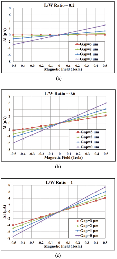
Figure 7 Differential current – magnetic field responses: (a) L/W = 0.2, (b) L/W = 0.6 and (c) L/W = 1.
Table 1 Relative sensitivity (T−1) at 0.25 mA, B = 0.5 T
| Gap(μm) | |||||
| L/W Ratio | 3 | 2 | 1 | 0 | |
| 0.2 | 0.2 | 0.0003 | 0.0036 | 0.0092 | 0.0231 |
| 0.6 | 0.0182 | 0.0264 | 0.0338 | 0.0479 | |
| 1 | 0.0326 | 0.0389 | 0.0481 | 0.0595 | |
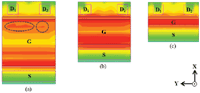
Figure 11 shows the current density distribution of non-split drain structure of the aspect ratios L/W 1, 0.6, and 0.2. The magnetic field is 0.5 T in the +z direction. It can be observed as the differential current distribution near the drain contact as shown in the circle of Figure 11(a). In this case, the sensitivity is high as shown in Figure 7. The current density increases when the aspect ratio is reduced or the channel is shorter than width as we can see in Figures 11(b) and 11(c). The differential current near the drain is hardly observed when the aspect ratios are reduced from 1 to 0.2 as shown in Figure 11. The sensitivity decreases with the reduced aspect ratio L/W directly. The sensitivity and aspect ratio relation is according to the standard equation of the MAGFET are [15].
| (9) |
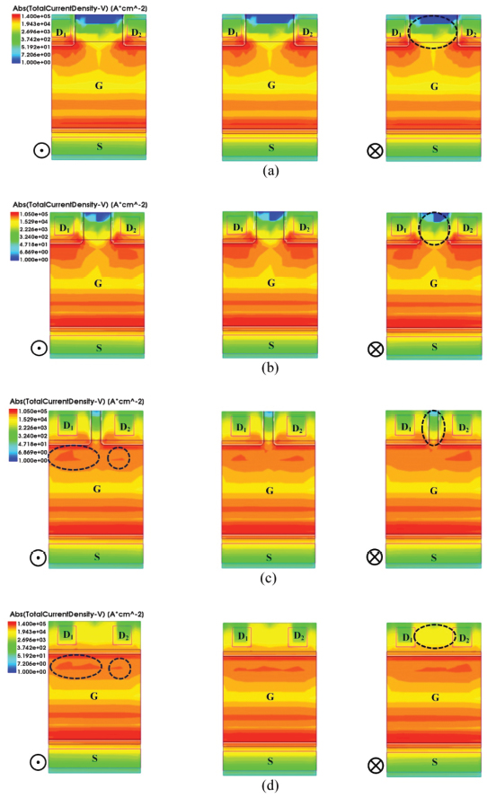
Figure 8 Current density distribution of MAGFET, L/W = 5 μm/5 μm = 1, BZ,−Z = 0.5 T: (a) Gap = 3 μm, (b) Gap = 2 μm, (c) Gap = 1 μm and (d) Gap = 0 μm.
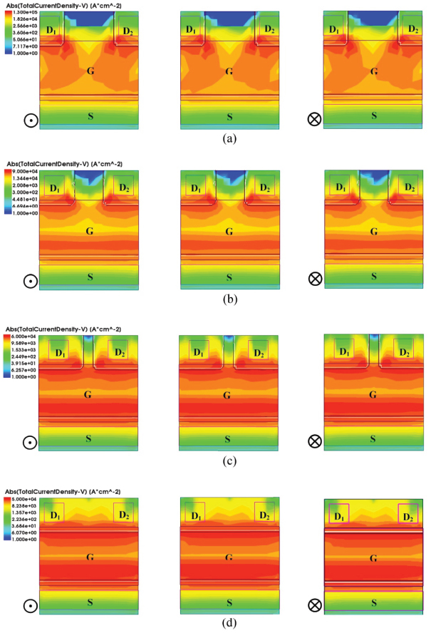
Figure 9 Current density distribution of MAGFET, L/W = 3 μm/5 μm = 0.6, BZ,−Z = 0.5 T: (a) Gap = 3 μm, (b) Gap = 2 μm, (c) Gap = 1 μm and (d) Gap = 0 μm.
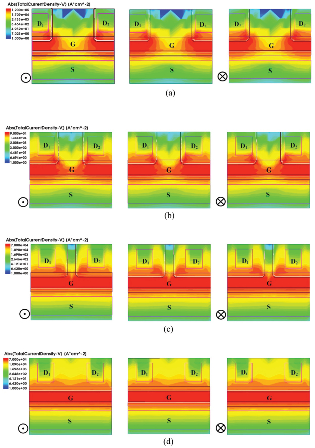
Figure 10 Current density distribution of MAGFET, L/W = 1 μm/5 μm = 0.2, BZ,−Z = 0.5 T: (a) Gap = 3 μm, (b) Gap = 2 μm, (c) Gap = 1 μm and (d) Gap = 0 μm.
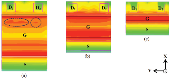
Figure 11 Current density distribution of MAGFET: (a) L/W = 1, (b) L/W = 0.6 and (c) L/W = 0.2.
where μch is the channel mobility, L the is gate length, W is the gate width, and GH is the geometrical factor. Normally GH is less than 1, and depends on the device geometry including the gap. The zero gap will enhance the GH approach to the ideal value. From the results of Figures 7 to 11, it can be said that the MAGFET does not need to design a gap between split drain structures as the conventional design. The non-split drain structure which has no gap will enhance the MAGFET approach to realize the ideal condition.
Proposed model
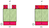
From the results, a simplified model for easier understanding is proposed. Figure 12 shows the comparison between the conventional split drain MAGFET and the proposed model of the non-split drain MAGFET that illustrates how the gap will make some loss. Figure 12(a) shows the case of the conventional design with gap; the electron currents are deflected by induced force to the left-hand side according to the magnetic field direction. The current of ID1 terminal should be ensured to be greater than ID2. As we can see in Figure 12(a), some electron current paths in the middle gap that should be deflected in D1 cannot deflect, and hence turn back to D2. This results in some losses and sensitivity decreases from the expected value and will have more effect when the gap is larger. If we observe the same condition with no gap design in Figure 12(b), we could see that the electron current deflection appears along the channel and continues within drain region. We can compare and observe the consistency of this model with the results of the current density distribution between contacts in Figure 8 and also in Figures 9 and 10. The amounts of current paths’ deflection from D2 to D1 of the new no-gap design are greater than the conventional gap design.

Figure 12 The comparison between (a) Split drain MAGFET and (b) Proposed model of non-split drain MAGFET.
By designing the MAGFET structure without gap or non-split drain MAGFET, it helps us to obtain the highest sensitivity that is ideal to the MAGFET structure because there is no loss from the gap. Nowadays, magnetic sensors with high efficiency are needed for wireless magnetic sensor nodes, which can be applied to monitor the status of a vehicle such as monitoring the amount of space in a parking lot, detecting the presence of a vehicle in a predetermined zone or real-time monitoring of traffic density data [16], and many other applications.
5 Conclusion
This is the first time to that we have proposed a new non-split drain MAGFET. It is a magnetic device that detects the vertical magnetic field similar to a conventional MAGFET. Its structure is the split drain MAGFET that has no gap between drains so that it has one drain with the two split contacts within a drain. The output differential current can be carried out by split contacts instead of the split drains of the conventional structure. This structure enhances the MAGFET to approach the ideal condition for the highest sensitivity of the same type of device with lossless from the gap. It is the simplest design for the highest sensitivity device which does not depend on any technological limitation. It can be applied to as the current mode devices which are compatible with low power, low voltage integrated systems for modern wireless sensor networks.
Acknowledgment
The authors would like to thank the National Research Council of Thailand for financial support of this research.
References
[1] Lenz and A. Edelstein, “Magnetic Sensors and Their Application”, IEEE Sensors Journal, Vol. 6 No. 3, 2006, pp. 631–649.
[2] A. Daubaras, M. Zilys, “Vehicle Detection based on Magneto-Resistive Magnetic Field Sensor”. Electronics and Electrical Engineering, Kaunas: Technologija, 2012, No. 2(118), pp. 27–32.
[3] Haji Said Fimbombaya, Nerey H. Mvungi, Ndyetabura Y. Hamisi and Hashimu U. Iddi, “Performance Evaluation of Magnetic Wireless Sensor Networks Algorithm for Traffic Flow Monitoring in Chaotic Cities”. Modelling and Simulation in Engineering Vol. 2018, Article ID 2591304, 11 pages.
[4] Vlada Velisavljevic, Eduardo Cano, Vladimir Dyo and Ben Allen, “Wireless Magnetic Sensor Network for Road Traffic Monitoring and Vehicle Classification”. Transport and Telecommunication, 2016, Vol. 17, No. 4, 274–288.
[5] Gerard F. Santillan-Quinonez, Victor Champac and Roberto S. Murphy, “Exploiting magnetic sensing capabilities of Short Split-Drain MAGFETs”, Solid-State Electronics 54 2010, pp. 1239–1245.
[6] Rodrigo Rodríguez-Torres and Edmundo A. Gutiérrez-Domínguez, “Analysis of Split-Drain MAGFETs”, IEEE Transactions on Electron Devices, Vol. 51, No. 12, December 2004, pp. 2237–2245.
[7] Z. Xiaofeng, W. Dianzhong, L. Meiwei, G. Hanyu and L. Gang, Fabrication and characterization of the split-drain MAGFET based on the nano-polysilicon thin film transistor, J. Semicond, Vol. 35, No. 9, 2014, pp. 094004-1–094004-6.
[8] Guo Qing, Zhu Dazhong and Yao Yunruo “CMOS magnetic sensor integrated circuit with sectorial MAGFET”, Sensors and Actuators A 126 2006, pp. 154–158.
[9] Shuk-Fun Lai, Wing-Kong Ng, Wing-Shan Tam, Chi-Wah Kok and Hei Wong “A Low Power CMOS Magnetic Field Sensor consisting of a MAGFET and a Pulse Width Modulated Readout Circuit” 2017 International Conference on Electron Devices and Solid-State Circuits (EDSSC), October 18–20, 2017, Hsinchu, Taiwan.
[10] J. Marek, D. Donoval, M. Donoval, M. Daricek “Analysis of Novel MagFET Structures for Built-in Current Sensors Supported by 3D Modeling and Simulation” ASDAM 2008, The Seventh International Conference on Advanced Semiconductor 315 Devices and Microsystems, October 12–16, 2008, Smolenice Castle, Slovakia.
[11] S. R. Ashwin, S. Sreejith, U. Sajeshkumar, “TCAD Design of Tunnel FET Structures and Extraction of Electrical Characteristics”, International Journal of Science and Research (IJSR) ISSN (Online): 2013, pp. 2319–7064.
[12] Maria-Alexandra Paun, Jean-Michel Sallese and Maher Kayal “Hall Effect Sensors Design, Integration and Behavior Analysis” Journal of Sensor and Actuator Networks 2(1):85–97 March 2013.
[13] Nebojša Janković, Sanja Aleksić and Dragan Pantić “Simulation and Modeling of Integrated Hall Sensor Devices” Proceedings of Small Systems Simulation Symposium 2012, NiŽ, Serbia, 12th–14th February 2012 pp. 85–92.
[14] TCAD Sentaurus Manual, sysnopsis®, version D-2016.03.
[15] R. S. Popovic, “Hall Effect Devices” 2nd ed., IoP Publishing Ltd., London, 2004.
[16] E. Sifuentes, O. Casas, and R. Pallas-Areny “Wireless Magnetic Sensor Node for Vehicle Detection With Optical Wake-Up” IEEE Sensors Journal, Vol. 11, No. 8, August 2011, pp. 1669–1676.
Biographies

Rattapong Nakachai received his B.S. degree in electrical engineering from the Kasetsart University, Thailand in 2003, and the M.S. degree in electronics engineering from the King Mongkut’s Institute of Technology Ladkrabang, Bangkok, Thailand in 2008. His research interest areas are electronics engineering, computer programming, and semiconductor devices and sensors.

Amporn Poyai received his B.Sc. degree in physics from the Silpakorn University, Bangkok, Thailand in 1991, the M.S. degree in electrical engineering from the King Mongkut’s Institute of Technology Ladkrabang, Bangkok, Thailand in 1994, and the Ph.D. degree in electrical engineering from the Katholieke University of Leuven, Leuven, Belgium in 2002. His research is emphasized on design, simulation, fabrication and characterization of semiconductor device, microfabrication technology, and integrated circuits. He worked at the Thai Microelectronic Center (TMEC) and now he is currently working at the Design & Engineering Consulting Service Center (DECC) as part of the National Science and Technology Development Agency (NSTDA), Thailand.

Toempong Phetchakul received his B.S. degree in electronic engineering, and the M.S. degree in electrical engineering from the King Mongkut’s Institute of Technology Ladkrabang, Bangkok, Thailand, and the D.Eng. degree in solid state device engineering from the Tokai University, Japan. His research interests are in design, simulation, fabrication and characterization of semiconductor device, and semiconductor sensors on integrated circuits. He is currently working at the Department of Electronics, Faculty of Engineering, King Mongkut’s Institute of Technology Ladkrabang, Bangkok, Thailand.
Journal of Mobile Multimedia, Vol. 16_1-2, 45–64.
doi: 10.13052/jmm1550-4646.16123
© 2020 River Publishers