A Novel Dual Magnetodiode for Wireless Sensor Networks
Chalin Sutthinet1, Amporn Poyai2, and Toempong Phetchakul1,*
1Department of Electronics, Faculty of Engineering, King Mongkut’s Institute of Technology Ladkrabang, Bangkok, Thailand
2Thai Microelectronics Center, Design & Engineering Consulting Service Center (DECC), National Science and Technology Development Agency (NSTDA), Thailand
E-mail: 57601042@kmitl.ac.th; amporn.poyai@nectec.or.th; toempong.ph@kmitl.ac.th
* Corresponding Author
Received 30 April 2020; Accepted 17 May 2020; Publication 17 August 2020
Abstract
This paper presents a new magnetodiode, the so-called dual magnetodiode, for wireless sensor application. The device is a current mode which can be integrated with a chip compatible with modern low power, low voltage integrated circuit (IC). The structure and operation are completely different from a conventional magnetodiode. The structure is composed of two p–n junctions in that one region is common and the others are split terminals for output of differential current. The underlying mechanism is carrier deflection by induced force from a magnetic field. The carriers are injected from the common region by forward bias. The defection carriers diffuse, deflect, and recombine along substrate through split terminals according to direction and density of the magnetic field linearly and symmetrically. From the comparison of complementary structure of the split cathode and the split anode structure of LD = 50 μm, the bias current 1 mA and magnetic field 0.5 T, the relative sensitivities (SR) are 11.01 and 11.19 T−1, respectively. This device is a simple p–n junction structure which is compatible with all micro/nanotechnology.
Keywords: p–n junction, magnetic sensor, carrier deflection, diode, magnetodiode, Lorentz’s force, TCAD.
1 Introduction
Sensors are very important devices for measurement system [1, 2], wireless sensor network [3, 4], interactive multimedia system [5], automation [6], robotics [7, 8], learning machine, internet of things (IoT) [9–11], artificial intelligence (AI), and other smart systems [12]. In general applications, magnetic sensors are used for measuring speed detection, proximity switching, positioning, current sensing, etc. The key feature of the magnetic sensor is that the sensor is in contactless switching mode; so, there is no wear on the contact, and hence ensures high reliability and long lifetime. When the magnetic sensors are used together in many units, it will result in a magnetic sensor network. From the advancement of wireless technology, multimedia communication, and intelligent systems, it has given rise to mobile multimedia sensor networks (MMSNs) or wireless multimedia sensor networks (WMSNs) [13] that have been applied in many applications, such as games, virtual reality, interactive multimedia, smart environment monitoring, intelligent transport system [14], autonomous driving, etc. Magnetic sensor is a kind of sensor that is used to detect magnetic energy or quantity and transfer to electrical energy by some phenomena. Among all phenomena, the Hall effect is one of the most popular effects to create magnetic devices [15, 16]. There are two modes of operation of the Hall effect, i.e., one is the Hall voltage mode and another is the Hall current mode. The Hall voltage mode is used to make the Hall plate device that changes magnetic field to the Hall voltage [17, 18]. This device is very popular in magnetic device group. The current mode is also used to make magnetoresistance device [19]. Unfortunately, this effect gives the percentage of magnetoresistance not so high for nonmagnetic material such as a semiconductor and metal material. The magnetic material exhibits the so-called anisotropic magnetoresistance effect. In these materials the magnetization vector determines the direction along which the current normally flows. Because it gives very high percent of magnetoresistance than magnetoresistance from nonmagnetic materials, we call the phenomenon as giant magnetoresistance (GMR) [20].
Although the Hall effect current mode for magnetoresistance is not as popular as the GMR, there are many device structures that adapt the Hall effect current mode for magnetic detection. A magnetotransistor uses the Hall current mode for emitter current to get deflected to a collector by induced Lorentz’s force from magnetic density [21, 22]. This device must use current to supply device for more than one terminal and it has at least four terminals [23]. There is a proposed three-terminal magnetotransistor but it is not a natural symmetrical device, and therefore one has to adjust offset by an external circuit before usage [24, 25]. It is not popular as the Hall plate device in voltage mode. Magneto MOSFET or MAGFET uses the MOS structure for detecting magnetic field [26, 27]. There are still some researches in progress in this regard until now. Magnetodiode uses the Hall effect current mode with two different surface recombination rate of interfaces and double injection of carriers [28]. Since it requires the two different interfaces, it is difficult to control properties which depend on fabrication process so much to be the same in each fabrication. It needs some voltage drop on the p–n junction and response to high magnetic field density. It is not a symmetrical device because of the two different surface recombination rates. Even though it is a simple two-terminal and a voltage supply device, it is not so popular and interesting right from the time of its introduction.
In this paper, the new structure and operation of a magnetodiode is proposed. This device uses the p–n junction diode for detecting magnetic field. The underlying mechanism is carrier deflection in bulk from the Hall effect current mode. The structure composes of two diodes in that one terminal is common and the others are split. The p–n junction is a basic structure that is compatible with all technologies. This will bring the magnetodiode back to the point of interest again, especially the current mode device which does not have a simple structure device to fabricate and operate like the Hall device in voltage mode. From the current trend of energy saving, low power, low voltage and low current, when the voltage is reduced, the Hall device operating in the voltage mode has a problem with decreasing sensitivity. Using the current mode will have a technological advantage in reducing size. A dual magnetodiode can be fabricated easily with P–N junction in bulk. Based on the basic mechanism of operation of the device, it will be used to design and develop a new generation of high efficiency device in the future.
2 Device Structure and Fabrication
The dual magnetodiode is fabricated and measured for this study. The structure and process of the device are discussed in this section. It will be seen that the dual magnetodiode is so different from a conventional magnetodiode even though it is constructed by a diode structure. The fabrication process is the fundamental process in a laboratory in an electronics department.
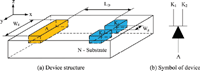
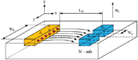
The structure of the device is shown in Figure 1(a). It is composed of one anode and two split cathodes. The symbol for the dual magnetodiode device is shown in Figure 1(b). The symbol is diode that has one anode and two cathodes. The distance between the cathodes is gap (Wg) and the distance from anode to cathode is length (LD). The substrate is an n-type silicon which is cathode and two separate ohmic contacts act as two separate cathodes. This structure is called the split cathode dual magnetodiode. The key parameters for this study are Wg and LD for which the ratios of W/L are 50/50 and 60/60 μm. The ohmic contact cathodes are square with the dimensions 50 × 50 μm2. The width of anode (WE) is equal the distance of the outer edges of the two cathodes. The dimensions are so large because they are designed and fabricated in a fundamental way in the laboratory as mention earlier. However, it is enough to prove the idea of the device and that it can be scaled down if it is fabricated with other technologies.
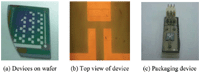
The device fabrication starts from an n-type silicon substrate with the resistivity 3–6 Ωcm. The anode P+ is formed by boron thermal diffusion and the split cathodes N+ and ohmic contacts are formed by phosphorus diffusion. The aluminum is evaporated and serves as etching substrate for device terminals. Figure 2(a) shows a photograph of complete fabricated devices on wafer and Figure 2(b) shows the top view layout of a complete device. The packaging of a device for measurement is shown in Figure 2(c).
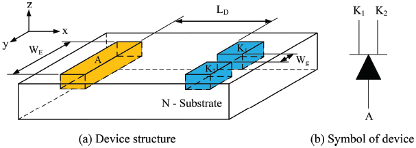
Figure 1 Split cathode dual magnetodiode structure.
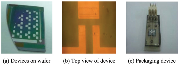
Figure 2 Photographs of dual magnetodiode.
3 Measurement and Results
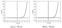
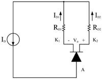
The devices were measured for electrical and magnetic responses. The p–n junction was investigated for its confirmation. Figure 3 shows the rectify characteristics of the p–n junction diode. It is tested by anode and each cathode to confirm the diode structure. The measurement circuit for magnetic responses is shown in Figure 4. A forward bias was applied via a constant current source which pushes current from anode to cathodes. This will keep total current (ID) constant in order to avoid any modulation from the magnetic field. The total current is sum of diode currents, ID1 and ID2, shown as
| (1) |
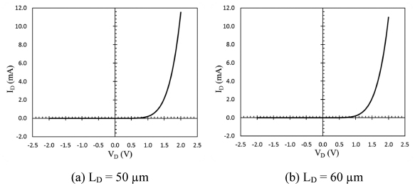
Figure 3 P–N junction I–V characteristics.

Figure 4 Measurement circuit for magnetic response.
The output Vo, the voltage between the two cathodes, can be expressed as
| (2) |
where RD1 = RD2 = RD and Equation (1) will become
| (3) |
and
| (4) |
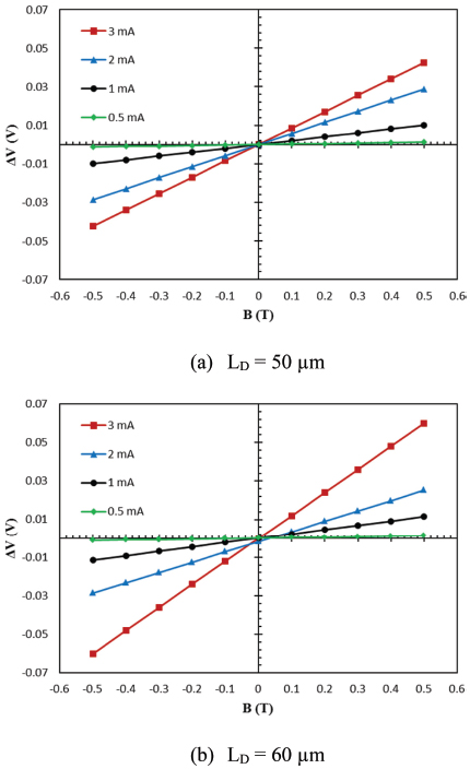
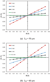
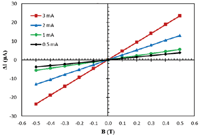
Figure 5 Magnetic responses of the split cathode dual magnetodiode.
The output voltages are amplified by an instrument amplifier. The output responses are measured as shown in Figure 5. They were applied in magnetic field density from 0 to 0.5 T perpendicular to the device surface in the Z and −Z directions as shown in Figure 1. The bias currents by constant current source were varied at 0.5, 1, 2, and 3 mA. Figure 5(a) shows the parameter of W = 50 μm and L = 50 μm. It is the plot between Vo and magnetic field density (B). The slope of the graph is defined as absolute sensitivity (SA) as shown hereunder:
| (5) |
From Figure 5(a), the linear dependence of Vo and B is observed. The biased currents affect sensitivity directly. The higher-biased current gives the higher sensitivity. The absolute sensitivities, SA, are 0.0025, 0.0200, 0.0575, and 0.085 mV/T at the biased currents 0.5, 1, 2, and 3 mA, respectively. The device can detect the direction of the magnetic field via symmetry responses.
Figure 5(b) is the response of the device parameter, i.e., W = 60 μm and L = 60 μm. The overall picture looks similar to the case in Figure 5(a). The sensitivities are 0.0025, 0.0230, 0.0540, and 0.1200 mV/T at the biased currents at 0.5, 1, 2, and 3 mA, respectively. Comparison of sensitivity between Figure 5(a) and Figure 5(b) forces one to think that the sensitivity value of Figure 5(b) is greater than Figure 5(a). The device still detects quantity and direction linearly and symmetrically.
4 Discussion
In this section we discuss about the proposed model for mechanism explanation. Experimental results will be confirmed not only by this model, but also by a simulation. Some aspects of this model are discussed and made clear by simulation results.
4.1 Proposed Model for the Split Cathode Dual Magnetodiode
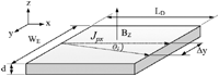
The dual magnetodiode operates via the forward bias p–n junction. The diffusion hole minority current density (Jpx) from hole carriers is injected from p-type to n-type and diffusion electron minority current density (Jnx) is injected from n-type to p-type and hence combined to total current JD as the diode current. It can be written as
| (6) |
| (7) |
| (8) |
where q is the electron charge, Dp and Dn are the diffusion coefficients of the hole and electron, respectively, Lp and Ln are the diffusion lengths of the hole and electron, respectively, k is the Boltzmann constant, T is the ambient temperature, and Va is the applied forward bias voltage.
From the practical diode fabrication, Jpx is much larger than Jnx, and in this structure at least 3 orders high according to the high p-type doping concentration greater than the n-type doping concentration. It is convenient to simplify as
| (9) |
The cathode’s currents (JD1 and JD2) are equal and balance with the value JD/2 as
| (10) |
When the magnetic field is applied in the z direction, Lorentz’s force is induced in y direction and the injected hole currents JD from the anode to cathode are deflected in the y direction. The carrier deflection effect by Lorentz’s force causes the cathode current JD2 to be greater than the JD1 created output differential current ΔID which is ID2 − ID1. This discussion can be concluded using the proposed model as shown in Figure 6.
Figure 7 shows the active area of current deflection where d is defined as depth of current according to current cross-sectional area. The carriers are deflected by Lorentz’s force causing the Lorentz’s angle ΘL, which is
| (11) |
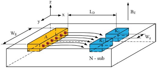
Figure 6 Proposed model for the split cathode dual magnetodiode when applied magnetic field in +Z direction.
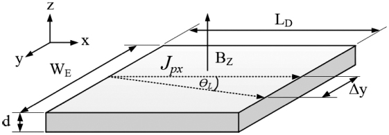
Figure 7 Active area of carrier deflection.
and
| (12) |
where μp is the hole mobility. The differential current ΔID is the integrating current density Jpx over the effective area d · Δy. It can be written as
| (13) |
By substituting Equation (12) in Equation (13), it will become as
| (14) |
The sensitivity (S) of the device is
| (15) |
The relative sensitivity (SR) is defined as the sensitivity per biased current (I) which is
| (16) |
Equation (15) indicates that the sensitivity of the device depends on biased current, the length between anode and cathode contact (LD), and mobility. Biased current is the term Jpx · d which is controlled by constant current source that is confirmed by experimental results from Figure 5. The length (LD) is confirmed by the results in Figures 5(a) and (b).
The cathode contact currents JD1 and JD2 are the electron majority drift currents Jn1 and Jn2 that will drift by electric field to support hole minority diffusion current Jpx which is recombined along the substrate and electron minority diffusion current Jnx which is injected from n-type to p-type through the p–n junction as shown in Equation (6). The two contact current densities when applied in the magnetic field in the z direction in terms of Equation (1) can be written as
| (17) |
| (18) |
where ΔJp is the deflection hole current, n is the electron carrier concentration at terminal, and A is cross-sectional area which is dΔy·. By using in the same way in Equations (11) to (13), we obtain
| (19) |
which is the same as shown in Equation (14).
4.2 Simulation of the Split Cathode and Split Anode Dual Magnetodiode
The proposed model will be confirmed by a simulation [29]. In this section, the structure of the split anode will be introduced. The simulation tool is Synopsys Sentaurus TCAD package program [30–32]. All semiconductor equations such as continuity, recombination, mobility, impurity ionization, and the Hall effect are available and used for simultaneous calculations [33–35]. It helps to save time and money in the study by the simulation method.
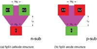
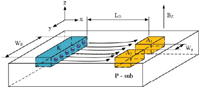
The device structures for simulation are shown in Figure 8. They consist of two basic structures: the split cathode in Figure 8(a) and the split anode in Figure 8(b). The structures have a modified design to have symmetry for each other in order to compare the performance. The common terminal is designed to have less space on both sides and placed in the middle to reduce losses and increase efficiency. The split cathode starts from the n-type substrate with the concentration of 1015 cm−3, whereas the p-type anode and n-doping split ohmic contact areas are doped with the same concentration of 1018 cm−3. In the same way, the split anode starts from the p-type substrate with the concentration of 1015 cm−3. The cathode is n-type with the concentration of 1018 cm−3, and two anodes are p-type with the concentration of 1018 cm−3. The parameter is the length between cathode and anode (LD) which is varied at 5, 10, 20, 30, 40, and 50 μm. The width between split contacts (Wg) is 5 μm and the substrate thickness is 1 μm. There is field oxide covered throughout all the area in addition to making the current path between anode and cathode.

Figure 8 Dual magnetodiode structures for simulation.
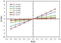
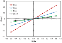
The magnetic responses of the split cathode in various parameters of LD are shown in Figure 9. The responses are linearly dependent with magnetic field density and length LD according to Equation (14). The device detects the density and direction of the magnetic field. The relative sensitivities at biased current 1 mA and magnetic field density 0.5 T are 0.987, 1.611, 2.870, 4.097, 8.076, and 11.01 T−1 for the deflection length LD 5, 10, 20, 30, 40, and 50 μm, respectively. Figure 10 shows the responses of the split cathode at various biased currents of deflection length LD = 50 μm. The relative sensitivities are 7.506, 11.09, 24.08, and 45.08 T−1 for the biased currents 0.5, 1, 2, and 3 mA, respectively. The more biased current increases the term Jpx · d in Equation (14).
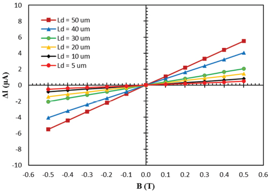
Figure 9 The magnetic responses of the split cathode at biased current 1 mA.
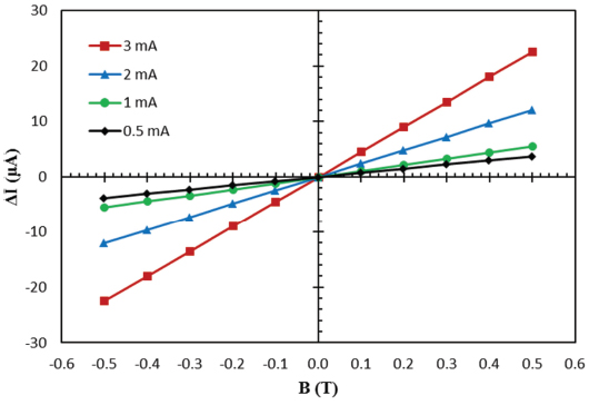
Figure 10 The magnetic responses of the split cathode of length LD = 50 μm.
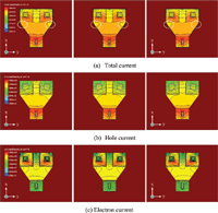
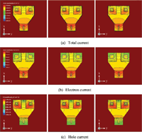
The two dimensional top view of current density distribution with applied magnetic field is shown in Figure 11. The current density distribution of conventional current, electron current, and hole current are shown in Figures 11(a), (b), and (c), respectively. The magnetic field is applied at 0.5 T and biased current is 1 mA. The left-hand side of Figure 11 is the case of applied magnetic field in −z direction, the right-hand side is the case of applied magnetic field in z direction, and in the middle is the case of no magnetic field. The conventional current flows from anode to two cathodes equally when no magnetic field is applied so that we can observe the symmetry color distribution in the middle of Figure 11(a). The current density is dense at anode contact and reduces from anode to cathodes and denser again at cathode contacts. When magnetic field is applied in the z direction, the Lorentz’s force induced in the y direction causes the current defects on the right-hand side as shown in the right-hand side of Figure 11(a). In a similar way, the current deflects on the left-hand side when magnetic field is applied in the −z direction. It is easier to observe these changes when observing the current distribution in circles that are made in Figure 11. Figure 11(b) is the case of hole current density. The holes are injected from the p-type anode to the n-type cathode and diffuse and recombine along the n-type cathode bulk. The hole current density is dense at anode contact and reduces from anode to cathode and denser again at cathode contacts. But the current density at cathode is less than anode because the anode current is recombined with electrons during diffusion in the n-type semiconductor, resulting in a reduced amount of hole diffusion current that we can observe in the current density of hole current at both anode and cathode in Figure 11(b). It differs from the conventional total current in Figure 11(a) because total current is created by the sum of electron and hole currents which are constant throughout the device, as we can observe from the current density at both anode and cathode in Figure 11(a). The hole current deflection due to magnetic field in the −z direction and z direction in Figure 11(b) is in the same way as that of the total current in Figure 11(a).
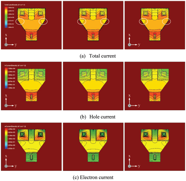
Figure 11 Current density distribution of the split cathode dual magnetodiode.
Figure 11(c) is the electron current density distribution. This electron current drifts by electric field from cathode to anode to compensate electrons that recombine with holes that are injected and diffuse from anode to cathode. The electron current density is dense at cathode and reduces from cathodes to anode and dense again at anode contact. We can observe this change from the current density of the anode and cathode in Figures 11(c) and 11(b). The electron current density, when magnetic field is applied in the z direction, results in the current density of cathode 2 (ID2) being greater than cathode 1 (ID1) because Lorentz’s force is induced in the y direction or electron current drifts to compensate for the hole current in cathode 2 being greater than the hole current in cathode 1.
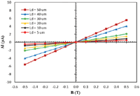
Figure 12 shows magnetic responses of the split anode that the parameter deflection lengths Ld are varied at 5, 10, 20, 30, 40, and 50 μm. The relative sensitivities at biased current 1 mA and magnetic field density 0.5 T are 0.989, 1.702, 2.936, 4.177, 8.106, and 11.19 T−1, respectively. Figure 13 shows the responses of the split anode at various biased currents of deflection length LD = 50 μm. The relative sensitivities are 7.606,11.18, 26.09, and 47.09 T−1 for biased currents 0.5, 1, 2, and 3 mA, respectively. The more biased current increases minority electron diffusion current density, Jnx. In the same way as split cathode, the differential output current ΔID in Equation (14) will become
| (20) |
The sensitivity of the device then becomes
| (21) |

Figure 12 The magnetic responses of the split anode at biased current 1 mA.
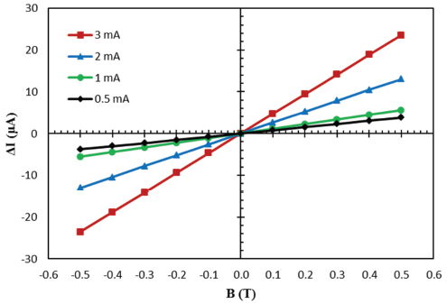
Figure 13 The magnetic responses of the split anode at length LD = 50 μm.
where μn is the electron mobility. The sensitivity in Equation (21) is the slope of graphs in Figures 12 and 13 which are the same sign as in the case of the split cathode because the differential current now is
| (22) |
The currents ID1 and ID2 flow into the anode terminals which are opposed to the split cathode case, and in which currents flow out of the cathode terminals. The current density distribution of total current JD from anode to cathode, hole majority drift current from anode to cathode to compensate for electron recombination in substrate, and electron minority diffusion current from cathode to anode are shown in Figures 14(a) to (c), respectively. The biased current is 1 mA and applied magnetic field is 0.5 T. The current density is symmetrical when no magnetic field is applied and deflected on the left-hand side for the applied magnetic field in the z direction which cause magnitude of ID1, (|−ID1|), greater than the magnitude of ID2, (|−ID2|). The currents are defected on the right-hand side for applied magnetic field in the −z direction as shown in Figure 14.
The proposed model for the split anode magnetodiode is shown in Figure 15. The magnetic field is applied in the +z direction. The device current is minority electron diffusion current injected from cathode to split anodes. This current diffuses and recombines along the current path in p-substrate. The split contact anode hole majority drift current flows to support the recombination current. The Lorentz’s force is induced in the −y direction and the conventional current JD of the device is in the −x direction. The current difference ΔID in Equation (22) and sensitivity in Equation (21) is positive again as in the case of the split cathode that are shown in Figures 9 and 12.
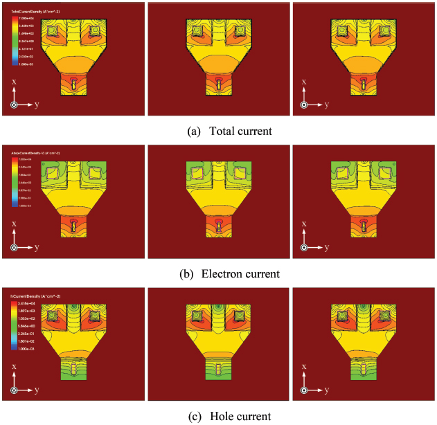
Figure 14 Current density distribution of the split anode dual magnetodiode.
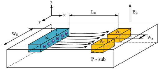
Figure 15 Proposed model for the split anode dual magnetodiode when applied magnetic field in +Z direction.
Magnetic sensors are important devices that are integrated into mobile devices [36] and activities of daily living (ADL). To improve the magnetic sensor so as to be highly effective, it must rely on a thorough study of the basic mechanism of the device. As a result of the proposed new structure, it can be used for design in the future for higher sensitivity, energy saving, and reduced size. It can be integrated into the IC, resulting in systems with a magnetic sensor such as the NodeMCU [37], wireless sensor networks (WSNs), IoT, multimedia sensor networks (MSNs), and virtual reality (VR) [38].
5 Conclusion
The new structure and mechanism of the magnetodiode are proposed. It is different from the conventional magnetodiode that used the two different surface recombinations. The structure is like a two p–n junction diode, i.e., the so-called dual magnetodiode in that one terminal is common and the others are split. There are two structures of the device, which are split anode and split cathode. The underlying mechanism is deflection of diffusion carriers that are injected from a common terminal through the p–n junction by Lorentz’s force which is induced linearly from magnetic field density cross with carrier conventional current. The diffusion current deflection causes the differential output current ΔID according to direction and density of magnetic field linearly and symmetrically. The device is the p–n junction structure that is compatible with all technologies including low power and low voltage IC. It is a device with high potential for current mode magnetic sensor that is exactly similar to the Hall plate in voltage mode magnetic device.
Acknowledgement
The authors would like to thank the National Research Council of Thailand for financial support of this research.
References
[1] O. Kanoun and H. Trankler, ‘Sensor technology advances and future trends’, IEEE Transactions on Instrumentation and Measurement, vol. 53, pp. 1497–1501, 2004.
[2] S. Shenghe, ‘Development trend of modern sensor’, Journal of Electronic Measurement and Instrument, vol. 1, pp. 1–10, 2009.
[3] L. Zheng, ‘Industrial wireless sensor networks and standardizations: The trend of wireless sensor networks for process automation’, Proceedings of SICE Annual Conference 2010, pp. 1187–1190, 2010.
[4] K. E. Skouby, I. William, and A. Gyamfi, Handbook on ICT in developing countries: 5G perspective: River Publishers, 2017.
[5] M. Chen, C.-F. Lai, and H. Wang, ‘Mobile multimedia sensor networks: architecture and routing’, EURASIP Journal on Wireless Communications and Networking, vol. 2011, p. 159, 2011.
[6] N. Derbel, F. Derbel, and O. Kanoun, Systems, Automation and Control: 2017 vol. 5: Walter de Gruyter GmbH & Co KG, 2017.
[7] H. F. Durrant-Whyte, Integration, coordination and control of multi-sensor robot systems vol. 36: Springer Science & Business Media, 2012.
[8] A. Ghorbel, M. Jallouli, L. Amouri, and N. B. Amor, ‘A HW/SW Implementation on FPGA of Absolute Robot Localization Using Webcam Data’, Sensors, Circuits & Instrumentation Systems, vol. 2, p. 75, 2017.
[9] J. Gubbi, R. Buyya, S. Marusic, and M. Palaniswami, ‘Internet of Things (IoT): A vision, architectural elements, and future directions’, Future generation computer systems, vol. 29, pp. 1645–1660, 2013.
[10] O. Vermesan and J. Bacquet, Next generation Internet of Things: Distributed intelligence at the edge and human machine-to-machine cooperation: River Publishers, 2019.
[11] A. Banafa, Secure and Smart Internet of Things (IoT): River Publishers, 2018.
[12] O. Vermesan and J. Bacquet, Cognitive Hyperconnected Digital Transformation: Internet of Things Intelligence Evolution: River Publishers, 2017.
[13] K. Sha, A. Striegel, and M. Song, Advances in Computer Communications and Networks: From Green, Mobile, Pervasive Networking to Big Data Computing: River Publishers, 2016.
[14] R. Chimata, R. Singh, and B. Singh, Internet of Things in Automotive Industries and Road Safety: River Publishers, 2018
[15] E. H. Putley, The Hall effect and semi-conductor physics, 1968.
[16] R. S. Popovic, Hall effect devices: magnetic sensors and characterization of semiconductors: CRC Press, 2004.
[17] E. Ramsden, Hall-effect sensors: theory and application: Elsevier, 2011.
[18] M. Crescentini, M. Biondi, A. Romani, M. Tartagni, and E. Sangiorgi, ‘Optimum design rules for CMOS Hall sensors’, Sensors, vol. 17, p. 765, 2017.
[19] Y. Chemthung, T. Phetchakul, and A. Poyai, ‘Effect of Horizontal Magnetic Field on Magnetoresistance’, 15th International Conference on Electrical Engineering/Electronics, Computer, Telecommunications and Information Technology (ECTI-CON2018), pp. 209–212, 2018.
[20] C. Reig, S. Cardoso, and S. C. Mukhopadhyay, ‘Giant magnetoresistance (GMR) sensors’, SSMI6, vol. 1, pp. 157–180, 2013.
[21] L. Davies and M. Wells, ‘Magneto-transistor incorporated in a bipolar IC’, Proc. ICMCST, Sydney, Australia, pp. 34–35, 1970.
[22] C. Riccobene, G. Wachutka, J. Burgler, and H. Baltes, ‘Operating principle of dual collector magnetotransistors studied by two-dimensional simulation’, IEEE Transactions on Electron Devices, vol. 41, pp. 1136–1148, 1994.
[23] Lj. Ristic M. Doan and M. Paranjape, ‘3-D Magnetic Field Sensor Realized as Lateral Magnetotransistor in CMOS Technology’, Sensor and Actuators, vols. A21–A23, pp. 770, 1990.
[24] C. Leepattarapongpan, T. Phetchakul, N. Penpondee, P. Pengpad, E. Chaowicharat, C. Hruanun, A. Poyai, ‘Magnetotransistor based on the carrier recombination–deflection effect’, IEEE Sensor Journal 10(2), pp. 294–299, 2010
[25] C. Leepattarapongpan et al., ‘A merged magnetotransistor for 3-axis magnetic field measurement based on carrier recombination–deflection effect’, Microelectron Journal, vol. 45, pp. 565–573, 2014.
[26] E. Yosry, W. Fikry, A. El-henawy, and M. Marzouk, ‘Compact model of dual-drain MAGFETs simulation’, Int. J. Electron. Commun. Comput. Eng, vol. 1, pp. 112–116, 2009.
[27] R. Nakachai, A. Poyai, and T. Phetchakul, ‘Non-Split Drain MAGFET’, 5th International Conference on Engineering, Applied Sciences and Technology (ICEAST), pp. 1–4, 2019.
[28] R. S. Popovic, H. P. Baltes, and F. Rudolf, ‘An integrated silicon magnetic field sensor using the Magnetodiode principle’, IEEE Transactions on Electron Devices, vol. 31, pp. 286–291, 1984.
[29] A. Nathan, A. M. J. Huiser, and H. P. Baltes, ‘Two-dimensional numerical modeling of magnetic-field sensors in CMOS technology’, IEEE Transactions on Electron Devices, vol. 32, pp. 1212–1219, 1985.
[30] Sentaurus Process User Guide, Mountain View, CA, USA: Synopsys Inc, 2016.
[31] Sentaurus Structure Editor User Guide, Mountain View, CA, USA: Synopsys Inc, 2016.
[32] Sentaurus Device User Guide, Mountain View, CA, USA: Synopsys Inc, 2016.
[33] K. Hess, Advanced theory of semiconductor devices, 2000.
[34] J.-P. Colinge and C. A. Colinge, Physics of semiconductor devices: Springer Science & Business Media, 2005.
[35] D. A. Neamen, Semiconductor physics and devices: basic principles: New York, NY: McGraw-Hill, 2012.
[36] I. M. Pires, N. M. Garcia, N. Pombo, F. Flórez-Revuelta, and S. Spinsante, “Data Fusion on Motion and Magnetic Sensors embedded on Mobile Devices for the Identification of Activities of Daily Living,” arXiv preprint arXiv:1711.07328, 2017.
[37] A. Maier, A. Sharp, and Y. Vagapov, “Comparative analysis and practical implementation of the ESP32 microcontroller module for the internet of things,” in 2017 Internet Technologies and Applications (ITA), 2017, pp. 143–148.
[38] W. Hongtao, Y. Zhimin, W. Ping, B. Santoso, and O. C. Lian, “A Novel Method of Motion Tracking for Virtual Reality Using Magnetic Sensors,” in 2018 Asia-Pacific Magnetic Recording Conference (APMRC), 2018, pp. 1–1.
Biographies

Chalin Sutthinet received his B.S. degree in electronic engineering from the Southeast Asia University, Bangkok, Thailand in 1995 and the M.S. degree in microelectronics engineering from the King Mongkut’s Institute of Technology Ladkrabang, Bangkok, Thailand in 2013.
His research interest areas are automation control engineering, internet of things, data science, artificial intelligence, virtual reality, semiconductor devices, and sensors.

Amporn Poyai received his B.Sc. degree in physics from the Silpakorn University, Bangkok, Thailand in 1991, the M.S. degree in electrical engineering from the King Mongkut’s Institute of Technology Ladkrabang, Bangkok, Thailand in 1994, and the Ph.D. degree in electrical engineering from the Katholieke University of Leuven, Leuven, Belgium in 2002.
His research is emphasized on design, simulation, fabrication and characterization of semiconductor device, microfabrication technology, and integrated circuit. He worked at the Thai Microelectronics Center (TMEC) and now is currently working at the Design & Engineering Consulting Service Center (DECC) as part of the National Science and Technology Development Agency (NSTDA), Thailand.

Toempong Phetchakul received his B.S. degree in electronic engineering, the M.S. degree in electrical engineering from the King Mongkut’s Institute of Technology Ladkrabang, Bangkok, Thailand, and the D.Eng degree in solid state device engineering from the Tokai University, Japan.
His research interests are in design, simulation, fabrication and characterization of semiconductor device, and semiconductor sensors on integrated circuit. He is currently working at the Department of Electronics, Faculty of Engineering, King Mongkut’s Institute of Technology Ladkrabang, Bangkok, Thailand
Journal of Mobile Multimedia, Vol. 16_1-2, 23–44.
doi: 10.13052/jmm1550-4646.16122
© 2020 River Publishers