Actively Simulated Floating Lossless Inductor for Short Range Wireless Communication
Pitchayanin Moonmuang1, Tattaya Pukkalanun1, Sumalee Unhavanich2 and Worapong Tangsrirat1,*
1Faculty of Engineering, King Mongkut’s Institute of Technology Ladkrabang (KMITL), Bangkok 10520, Thailand
2Faculty of Digital Technology, Chitralada Technology Institute, Bangkok 10300, Thailand
E-mail: worapong.ta@kmitl.ac.th
* Corresponding Author
Received 01 May 2020; Accepted 14 May 2020; Publication 24 July 2020
Abstract
This communication describes the resistorless simulation of the floating lossless inductor using three voltage differencing buffered amplifiers (VDBAs) and one grounded capacitor. The circuit employs only a grounded capacitor, and no other extra resistor element is employed. Thus, it is suitable for further communication integrated front-end circuit design in short-range wireless and application. The realized equivalent inductance value of the simulated inductor can be changed electronically via the external biasing currents of the VDBAs. Sufficient simulation results with the PSPICE program are provided to validate the functionality of the realized inductor. In addition to establishing the practical operation of the simulator, the measured test results obtained from hardware implementation using readily available integrated chips (ICs) are also included.
Keywords: Communication circuits and devices, short range wireless communication, near-field communication, inductance simulator, voltage differencing buffered amplifier (VDBA).
1 Introduction
In the last decades, LC filters are an important building block of modern communication electronic architecture [1]. It is also well known that every communication system and wireless application requires one or more filters in their circuit structure. The LC filter in the communication front-end section performs a significant part for controlling the selective frequency band of wireless standard, and eliminating the unwanted frequency band. In addition, discrete inductors find several applications in active filters, LC oscillators and comparators for impedance matching, parasitic cancellation and phase shifters [2]. For short range wireless communication, they are employed to appropriately tune and couple the front-end module and power amplifiers. They are also used to form the impedance matching in the near field communication circuit. However, from the viewpoint of the communication integrated circuit (IC) design, the major restrictions of the use of physical spiral inductors are their bulky structure, and small and non-tuneable inductance values. Therefore, it is highly preferable to simulate floating inductors with modern electronic active building blocks. Over the years, several floating lossless inductance simulator circuits have been designed using different types of active building blocks [6–14]. However, some of the inductance simulator circuits are realized with two kinds of active building blocks [4, 8–10]. The configurations reported in Refs. [5, 7, 11–13] require two active and three passive components for realizing floating lossless inductance simulators. In Refs. [3, 5–8, 10–14], many external passive resistors are employed for their realizations. In addition, in Refs. [3, 5–7, 10, 11] a floating resistor is used, which is not desirable for the IC fabrication. Furthermore, the floating lossless inductor realizations reported in Refs. [3, 5–7, 10–12] do not possess electronic tuning capability.
Recently, the novel reported active building block the so-called voltage differencing buffered amplifier (VDBA) has been proved to be a useful and versatile active element in realizing a class of analogue signal processing circuits and applications [17–20]. In the following sections, we focus our attention on the floating lossless inductor simulation realization based on the VDBAs, designed with a single grounded capacitor. The circuit comprises only three VDBAs and one grounded capacitor without using any external resistor component. The simulated equivalent inductance value can be regulated electronically through the adjustment of the external bias currents of the VDBAs. A detailed analysis of the VDBA non-ideal parameters and sensitivity performance are investigated. The functionality of the proposed simulator is illustrated by the PSPICE simulation results based on complimentary metal–oxide–semiconductor (CMOS) VDBA implementation using TSMC 0.25-μm CMOS technology process parameters. In addition to confirming the claimed idea, the practical results using commercially available LT1228 IC chips are also incorporated.
2 Proposed Floating Lossless Inductance Simulator
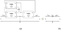
The proposed floating lossless inductance simulator circuit using three VDBAs and one grounded capacitor is shown in Figure 1(a). According to the standard notation, the terminal relations of the VDBA element can be defined as
| (1) |
where gm is an effective small signal transconductance gain of the VDBA. The parameters α and β are the non-ideal transconductance gain and the non-ideal transfer voltage gain, respectively. In an ideal case, the parameters α and β are equal to unity. Based on the behaviour relation (1) of the VDBA and an analysis of the circuit in Figure 1(a) with gm = gm1 = gm2 results in the following input impedance
| (2) |
This implies that the proposed circuit simulates a floating lossless inductor with the equivalent inductance value expressed as
| (3) |
It is clear that the value of Leq is feasible by electronic means through the gmgm3 product, and the equivalent model of this configuration is modelled in Figure 1(b).
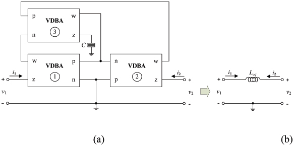
Figure 1 Proposed floating lossless inductance simulator circuit.
3 Non-ideal Analysis and Sensitivity Performance
If the non-ideal transconductance gain α and the non-ideal transfer voltage gain β of the VDBA are taken into consideration, then the expressions for the non-ideal Zin of the circuit in Figure 1(a) are obtained as follows
| (4) |
and
| (5) |
The relative sensitivities of Leq regarding active and passive components are found as
| (6) |
| (7) |
| (8) |
and
| (9) |
Since the absolute values of all sensitivity coefficients are no more than unity, the circuit exhibits low sensitivity performance.
4 Simulation Results
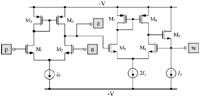
To reveal the performance of the proposed VDBA-based floating lossless inductance simulator in Figure 1(a), the simulations based on the PSPICE program have been carried out. In the simulations, the CMOS VDBA depicted in Figure 2 [18, 20] was employed using the TSMC 0.25-μm CMOS process model parameters. The bias voltage and the bias current were set as +V = -V = 0.75 V and IA = 50 μA. The aspect ratios (W/L) of the transistors in Figure 2 are the same as provided in Refs. [18, 20].
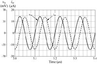
The proposed floating lossless inductance simulator in Figure 1(a) was simulated with the following circuit component values: gm1 = gm2 = gm3 = 1.58 mA/V (IB1 = IB2 = IB3 = 100 μA) and C = 100 pF. Therefore, the value of an equivalent inductance equal to Leq ≅ 40 μH is obtained. Figure 3 shows the simulated transient waveforms for the input voltage (vin=v1 − v2) and the input current (iin = i1 = −i2) of the simulator with 50 mV (peak) input voltage at 10 MHz. The simulation result shows the phase difference between vin and iin of about 89°, which is nearly close to the predicted value equal to 90°.
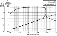
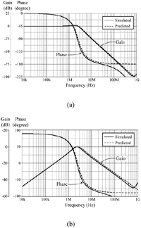
With the same component values, the simulated frequency responses of the input impedance (Zin) of the proposed inductance simulator, which are compared with the predicted responses, are also plotted in Figure 4. From these results, it can be noticed that, for the frequency range between 50 kHz and 30 MHz, the maximum errors in magnitude and phase are found to be approximated as 22% and 15%, respectively. Additionally, the total power consumption of the simulator is measured as 1.13 mW.
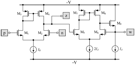
Figure 2 CMOS internal structure of the VDBA used in simulations [18, 20].
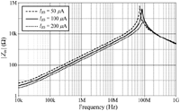
In order to further testify the electronic tuning capability of the circuit, the plots of |Zin| against frequency characteristics are given in Figure 5 for gm1 = gm2 = 1.58 mA/V and C = 100 pF and three different values of gm3, i.e., gm3 = 1.12 mA/V, 1.58 mA/V and 2.24 mA/V (IB3 = 50 μA, 100 μA and 200 μA). These designed component values are in accordance with the simulated equivalent inductance values of Leq = 56 μH, 40 μH and 28 μH, respectively. It is clearly demonstrated that, for different values of transconductance gm3, the value of Leq can be changed electronically.
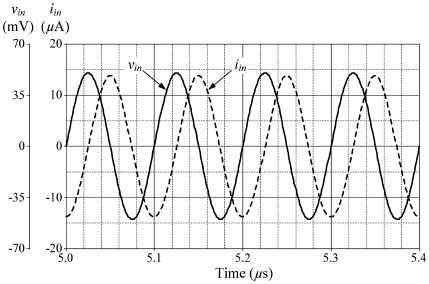
Figure 3 Transient response analysis of the proposed lossless inductor in Figure 1(a) for 10-MHz sinusoidal input voltage of 50 mV (peak).
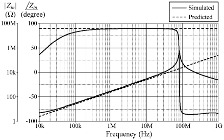
Figure 4 Frequency response analysis of the proposed lossless inductor in Figure 1(a).
5 Experimental Test Results
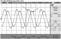
To affirm the earlier given theoretical predictions, the experimental test results have been also performed through the hardware implementation of the VDBA using the commercially available IC LT1228 [21]. It may be further noted that the LT1228 only based implementation of the VDBA provides the possibility of tuning gm with the external bias current IB, namely gm = 10IB. The printed circuit board (PCB) used in the experimental measurements of the proposed floating lossless inductor is pictured in Figure 6. The symmetrical supply voltages used were ±5 V. For all real measurements, the element values of the synthetic inductance simulator were set to gm1 = gm2 = 1 mA/V (IB1 = IB2 = 100 μA), and C = 1 nF. The measured waveforms of vin and iin through the proposed simulator are given in Figure 7 with 200-kHz sine wave input voltage of 50 mV (peak). In this measurement, the transconductance gm3 = 1 mA/V is chosen to obtain the synthetic inductor with Leq = 1 mH. As expected, it can be recorded from the graphs that the phase of iin lags that of vin by 88.1°, where the theoretical value is equal to 90°.
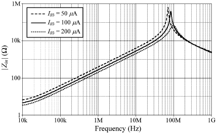
Figure 5 Magnitude frequency responses of the proposed lossless inductor in Figure 1(a) with tuning gm3 (IB3).
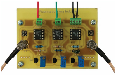
Figure 6 Fabricated PCB of the proposed floating lossless inductor in Figure 1(a).
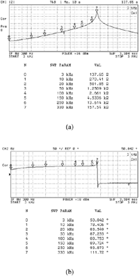
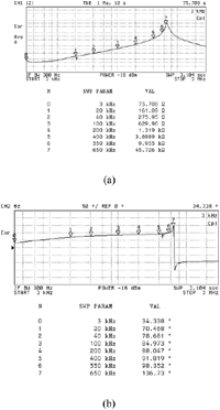
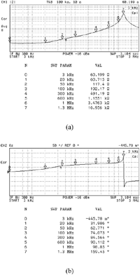
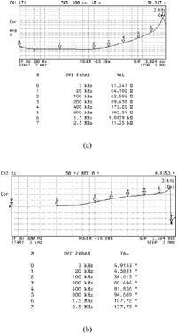
Likewise, the measurement data of the impedance-frequency characteristics of the proposed floating lossless inductor for gm3 = 0.5 mA/V, 1 mA/V, 2 mA/V and 5 mA/V (IB3 = 50 μA, 100 μA, 200 μA and 500 μA) are respectively given in Figures 8–11. For the given component values using Equation (3), the corresponding equivalent inductance values are obtained as Leq = 2 mH, 1 mH, 0.5 mH and 0.2 mH, respectively. It is noticeable that the experimental test results given in Figures 8–11 actualize the practical behaviour of the proposed floating synthetic lossless inductor.
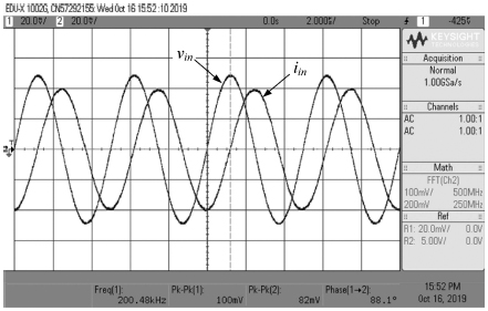
Figure 7 Measured results for the waveforms vin and iin of the proposed lossless inductor with 200-kHz sinusoidal input voltage of 50 mV (peak).
6 Applications to Filter Realization
To demonstrate the behaviour of the proposed floating lossless inductance simulator circuit of Figure 1, the same is employed to replace the passive inductors of the lowpass (LP) and bandpass (BP) filters given in Figures 12(a) and 12(b), respectively. In the circuit realization, the following passive components have been selected as RLP = RBP = 632 Ω and CLP = CBP = 100 pF. Further, an effective inductance of Leq ≅ 40 μH was implemented with the proposed inductor of Figure 1(a). Its component values are the same as that mentioned in Section 4. In this setting, the important frequency characteristics are obtained as fo = ωo/2π = 1/(LeqCLP)1/2 = 1/(LeqCBP)1/2 ≅ 2.52 MHz and Q = (1/RLP)(Leq/CLP)1/2 = (1/RBP)(Leq/CBP)1/2 = 1. Figure 13 shows the simulated frequency responses of both filters of Figure 12, compared with that of ideal floating inductors. It can be observed that the simulated values exhibit excellent agreement with theoretical results over a wide range.
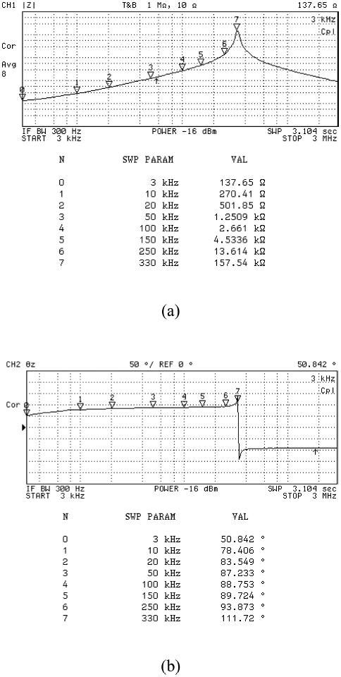
Figure 8 Experimental results of the impedance-frequency responses for gm3 = 0.5 mA/V. (a) magnitude response and (b) phase response.
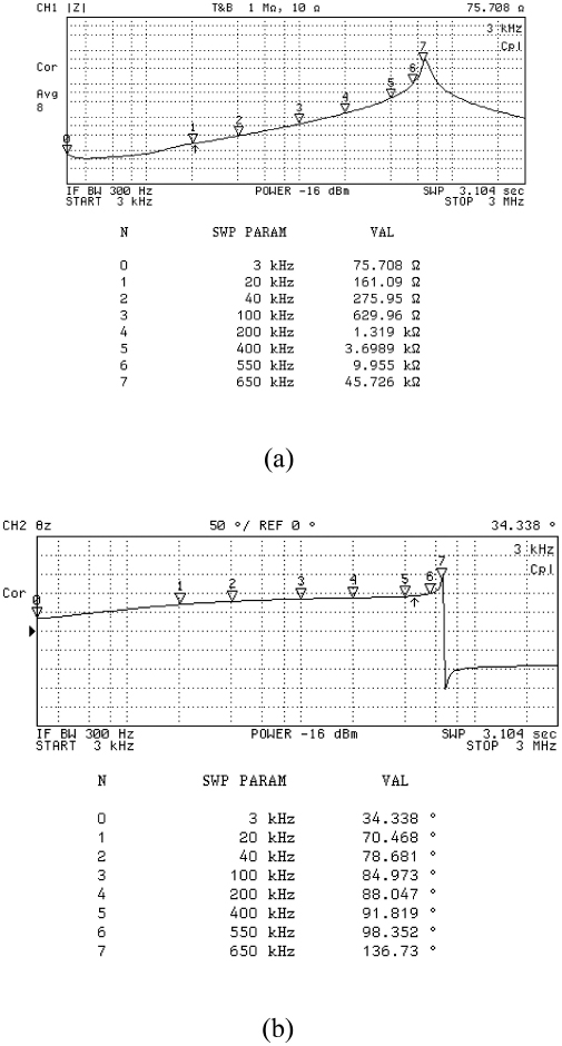
Figure 9 Experimental results of the impedance-frequency responses for gm3 = 1 mA/V. (a) magnitude response and (b) phase response.
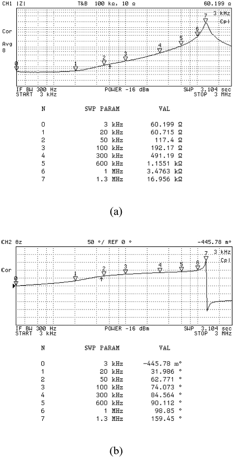
Figure 10 Experimental results of the impedance-frequency responses for gm3 = 2 mA/V. (a) magnitude response and (b) phase response.
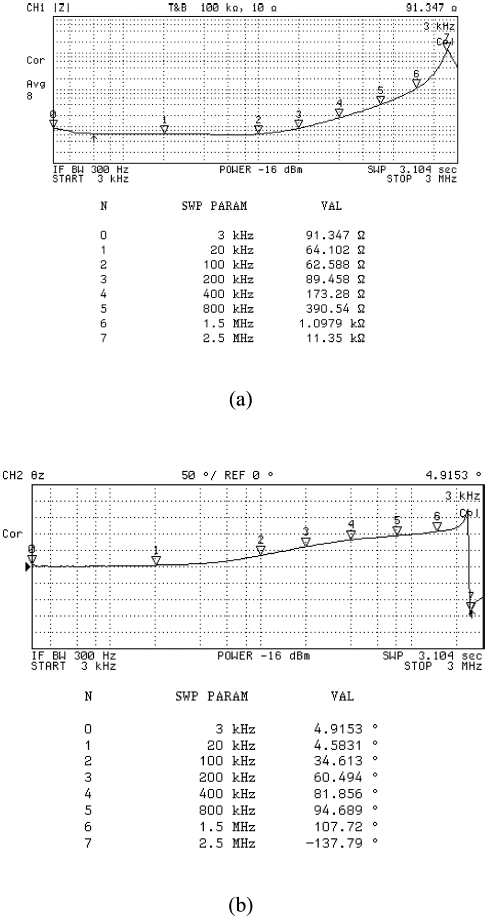
Figure 11 Experimental results of the impedance-frequency responses for gm3 = 5 mA/V. (a) magnitude response and (b) phase response.
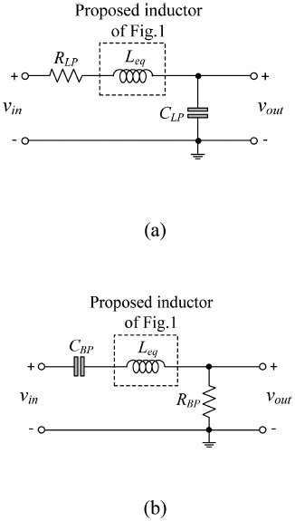
Figure 12 RLC filter realizations using the proposed inductor in Figure 1. (a) lowpass filter and (b) bandpass filter.
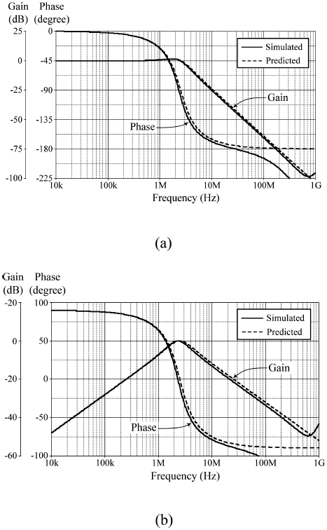
Figure 13 Theoretical and simulated frequency responses of the filters in Figure 12. (a) lowpass filter and (b) bandpass filter.
7 Concluding Remarks
In this work, the floating lossless inductance simulator consisting of three VDBAs and one grounded capacitor is developed. The proposed synthetic lossless inductor provides the following advantages: (i) no employment of any external resistor element, (ii) the use of only grounded capacitor as preferred for integration, (iii) simulated equivalent inductance can be scaled electronically through transconductance gains of the VDBAs and (iv) low active and passive sensitivity indexes. Applications of the proposed floating inductance simulator circuit in the RLC LP and BP filter realizations have also been outlined. A number of PSPICE simulation and experimental test results has been performed to validate the behaviour of the proposed inductance simulator. Therefore, the proposed circuit may be used to the design of highly integrated communication systems, since several filtering functions had to be performed off-ship. In the future, as the number of smart mobile phone and other miniature multimedia device products would have been dramatically increasing, the proposed active inductor circuit is expected to be useful in short range wireless communication and application.
Acknowledgements
This work is supported by the Faculty of Engineering, King Mongkut’s Institute of Technology Ladkrabang under the contract number 2563-02-01-033. The authors also gratefully acknowledge Assistant Professor Dr. Sathaporn Promwong, the coordinating guest editor of the special issue on Smart Innovative Technology for Future Industry and Multimedia Application, for useful information of this special issue.
References
[1] V. S. Kumar, S. Ramesh, ‘LCP based planar high Q embedded band pass filter for wireless applications’, J. Mobile Multimedia, vol. 14, no. 3, pp. 307–318, 2018.
[2] D. Harjunowibowo, R. W. Hastuti, K. A. Ratopo, A. Jamaluddin, S. Annur, ‘Simple blocking oscillator performance analysis for battery volateg enhancement’, J. Mobile Multimedia, vol. 11, no. 3&4, pp. 321–329, 2015.
[3] W. Kiranon, P. Pawarangkoon, ‘Floating inductance simulation based on current conveyors’, Electron. Lett., vol. 33, pp. 1748–1749, 1997.
[4] E. Yuce, S. Minaei, O. Cicekoglu, ‘Resistorless floating immittance function simulators employing current controlled conveyors and a grounded capacitor’, Electri. Eng., vol. 88, pp. 519–525, 2006.
[5] S. Minaei, E. Yuce, O. Cicekoglu, ‘A versatile active circuit for realising floating inductance, capacitance, FDNR and admittance converter’, Analog Integr. Circ. Signal Process., vol. 47, no. 2, pp. 199–202, 2006.
[6] E. Yuce, ‘On the implementation of the floating simulators employing a single active device’, Int. J. Electron. Commun. (AEU), vol. 61, no. 7, pp. 453–458, 2007.
[7] E. Yuce, S. Minaei, ‘A modified CFOA and its applications to simulated inductors, capacitance multipliers, and analog filters’, IEEE Trans. Circuits Syst I: Reg. Papers, vol. 55, no. 1, pp. 266–275, 2008.
[8] M. Sagbas, U. E. Ayten, H. Sedef, M. Koksal, ‘Floating immittance function simulator and its applications’, Circuits Syst. Signal Proces., vol. 28, no. 1, pp. 55–63, 2009.
[9] M. Sagbas, U. E. Ayten, H. Sedef, M. Koksal, ‘Electronically tunable floating inductance simulator’, Int. J. Electron. Commun. (AEU), vol. 63, no. 5, pp. 423–427, 2009.
[10] E. Yuce, S. Minaei, ‘Novel floating simulated inductors with wider operating-frequency ranges’, Microelectron. J., vol. 40, no. 6, pp. 928–938, 2009.
[11] J. W. Horng, ‘Lossless inductance simulation and voltage-mode universal biquadratic filter with one input and five outputs using DVCCs’, Analog Integr. Circ. Signal Process., vol. 62, no. 3, pp. 407–413, 2010.
[12] E. Yuce, ‘A novel floating simulation topology composed of only grounded passive components’, Int. J. Electron., vol. 97, no. 3, pp. 249–262, 2010.
[13] U. E. Ayten, M. Sagbas, N. Herencsar, J. Koton, ‘Novel floating general element simulators using CBTA’, Radioengineering, vol. 21, no. 1, pp. 11–19, 2012.
[14] D. Prasad, J. Ahmad, ‘New electronically-controllable lossless synthetic floating inductance circuit using single VDCC’, Circuits Syst., vol. 5, pp. 13–17, 2014.
[15] F. Kacar, A. Yesil and A. Noori, ‘New CMOS realization of voltage differencing buffered amplifier and its biquad filter applications’, Radioengineering, vol. 21, no. 1, pp. 333–339, 2012.
[16] O. Channumsin and W. Tangsrirat, ‘Single VDBA-based phase shifter with low output impedance’, Proc. of ECTI-CON’17, Phuket, Thailand, 27–30 Jun, 2017.
[17] A. Yesil, F. Kacar and K. Gurkan, ‘Lossless grounded inductance simulator employing single VDBA and its experimental band-pass filter application’, Int. J. Electron. Commun. (AEU), vol. 68, pp. 143–150, 2014.
[18] W. Tangsrirat, ‘Synthetic grounded lossy inductance simulators using single VDIBA’, IETE Journal of Research, vol. 63, pp. 134–141, 2017.
[19] W. Tangsrirat, O. Channumsin, ‘Tunable floating capacitance multiplier using single fully balanced voltage differencing buffered amplifier’, J. Commun. Tech. Electron., vol. 64, no. 8, pp. 797–803, 2019.
[20] W. Tangsrirat, ‘Actively floating lossy inductance simulators using voltage differencing buffered amplifiers’, IETE Journal of Research, vol. 65, no. 4, pp. 446–459, 2019.
[21] Linear Technology, “100MHz Current Feedback Amplifier with DC Gain Control”, LT1228 datasheet, (http://www.linear.com/product/L T1228).
Biographies

Pitchayanin Moonmuang received her B. Eng. degree (Honors) in Electronics Engineering, and M. Eng. degree in Control Engineering both from the Faculty of Engineering, King Mongkut’s Institute of Technology Ladkrabang (KMITL), Bangkok, Thailand, in 2016 and 2019, respectively. During her masters, she created several adjustable capacitance multiplier circuits, which resulted in conference presentations and published papers. She is currently a doctoral student in Electrical Engineering at KMITL. Pitchayanin’s current research revolves mostly around the areas of immittance function simulators and active analog filter design.

Tattaya Pukkalanun received the B.Eng.(Honors) degree in Control Engineering from King Mongkut’s Institute of Technology Ladkrabang (KMITL), Thailand, in 1998, M.Sc. degree in Advanced Electronic Engineering (with Distinction) from the University of Warwick, UK, in 2001, and M.Eng. and D.Eng. degrees in Electrical Engineering from KMITL in 2003 and 2010, respectively. Currently, she is an Associate Professor at the Department of Instrumentation and Control Engineering, Faculty of Engineering, KMITL. Her research areas include analog circuit design, signal processing and electronic control engineering.

Sumalee Unhavanich is an Associate Professor in the Faculty of Digital Technology at the Chitralada Technology Institute. Dr. Sumalee completed her D.Eng. degree in Electrical Engineering from King Mongkut’s Institute of Technology Ladkrabang (KMITL) and her undergraduate studies at King Mongkut’s University of Technology North Bangkok (KMUTNB). Her research interests lie in the area of electronic instrumentation and control system design, and analog signal processing applications.

Worapong Tangsrirat received the B.Ind.Tech. degree (Honors) in Electronics Engineering, and M.Eng. and D.Eng. degrees in Electrical Engineering all from Faculty of Engineering, King Mongkut’s Institute of Technology Ladkrabang (KMITL), Bangkok, Thailand, in 1991, 1997, 2003, respectively. Since 1995, he has been a faculty member at KMITL, where he is currently a Full Professor in Electrical Engineering at the Department of Instrumentation and Control Engineering. Presently, he is also an Executive Vice Dean Research and Innovation of the Faculty of Engineering, KMITL. Professor Worapong’s research interests are primarily in the areas of analog signal processing and integrated circuits, current-mode circuits, and active filter and oscillator design. He has edited or written 15 books, and has had more than 100 research articles published in peer reviewed international journals.
Journal of Mobile Multimedia, Vol. 15_4, 321–338.
doi: 10.13052/jmm1550-4646.1543
© 2020 River Publishers