Geometrical Requirement Analysis of RF-MEMS Switch
Edan Khan, Kennedy Sarangapani* and Dev Sparsh Sangwan
Department of Mechanical Engineering, Sharda School of Engineering and Technology, Sharda University, Greater Noida, India
E-mail: edan.khan8@gmail.com; kennedy.s@sharda.ac.in; devsparshsangwan11@gmail.com
*Corresponding Author
Received 08 January 2025; Accepted 01 May 2025
Abstract
Radio Frequency Micro-Electromechanical Systems (RF MEMS) have rapidly advanced over the past two decades. The integration of MEMS components in RF devices has met the demand for miniaturized components, resulting in compact devices with low power consumption and enhanced RF performance at higher frequencies. The control electrode has both metal-metal contact as well as metal-dielectric later contact in the Co Planer Waveguide (CPW). Besides the intrinsic stress due to the material property and the defects due to processing, the mismatch in the material properties between two different metals in the bimetallic structure affects the reliability of RF cantilever MEMS. For this study, silicon and gold are chosen for bimetallic structure and the deflection, sensitivity, and stiffness of both materials are analyzed to estimate the mismatch between them. Typical cantilever MEMS structures have been used with the dimension of length varying from 100 m to 300 m and the width and thickness of 10m. The mismatch in deflection, stiffness, and sensitivity between gold and silicon are the important parameters considering the operational limits of RF MEMS. MEMSolver 3.0 is used to calculate the deflection. The assumptions considered during the analysis were uniform beam cross section and the mass of the beam is negligible compared to the load.
Keywords: RF-MEMS, deflection, sensitivity, stiffness, mechanical analysis, geometry.
1 Introduction
MEMS systems have revolutionized various industries due to their compact size and versatile functionality. In bio sensing, MEMS technology facilitates swift and precise detection of biological analysis, supporting medical diagnoses and treatments. MEMS-based biosensors offer label-free detection, enhancing early disease detection and personalized medicine. In healthcare, MEMS devices enable continuous patient monitoring and telemedicine, significantly improving healthcare outcomes [1, 2].
MEMS switches are crucial components found in most RF devices. Over the past few decades, they have been employed in resonators, phase-shifters, sensors, reconfigurable antenna designs, satellite systems, communication systems, and radar applications. The first switches were designed to fully meet the requirements of steel electromagnetic relays. Despite years of advancements, modern RF electromagnetic relays, while offering low signal loss and high isolation in the off state, still face drawbacks such as large size, high cost, and limited lifespan [3]. Besides the functional design and fabrication and testing phases, the design optimization of MEMS plays a crucial role. The primary phase of analytical methods combines geometrical and materials properties to understand the system behavior. Various analytical methods such as partial differential equations, finite element analysis, boundary element analysis are used in analytical methods. With increasing requirement for accuracy, the level of complexity of the system increases. Cantilever type switched require minimum pull in voltages for its actuation, whereas these have reliability issues like stiction because of its metal to metal contact fracture, wear and delamination, exposure to vibration and shocks, thermal stresses and defects due to processing and packaging are the causes of failure of RF MEMS [6]. Main objective of this work is to analyze the effect of geometrical dimensions of the cantilever based RF MEMS in minimizing the mismatch between silicon and gold. This present work uses the simple cantilever beam design approach to analyze the mechanical features of the MEMS structure.
2 Methodology
When designing switches, it is essential to consider various parameters including RF performance, actuation voltage, and the stress produced. One of the most widely used techniques for selecting appropriate materials in RF MEMS switches is Ashby’s approach [6]. This method evaluates materials based on three parameters: functional, geometrical, and material properties. The methodology employs an equation tailored for the specific system under consideration. P f (Function Requirements ’F’, Geometric Requirements ‘G’, Material Requirements ‘M’) [4]. Various metals such as silicon, gold, silver, platinum, copper, aluminum etc. and dielectric materials such as SiO2, SrTiO3, HFO2, TiO2, Si3N4 have been used as RF MEMS switch components [5]. In this analysis silicon and gold are used as micro-cantilever beam material. The elastic and inelastic properties of gold in addition to strength makes it suitable material. Gold being a low resistive material, it is efficient in shunting RF current to the ground. With the combination of appropriate mechanical, electrical, thermal and chemical properties gold is preferred over other materials. Simple cantilever beam with free at one end structure is chosen for the analysis. The length is varied from 100 m to 300 m and the width is varied from 10 m to 30 m keeping the thickness constant. MEMSolver v3.3 is used to calculate deflection. The following assumptions such as beam of uniform cross section, mass of the beam is negligible in comparison to the end load were considered for carrying out the analysis. In this structure the maximum stress is at the free end of the cantilever beam.
The Sensitivity and stiffness were calculated using equations [7]:
| (1) | |
| (2) |
where I Moment of Inertia and E Young’s Modulus
| (3) |
3 Results and Discussion
Tables 1 and 2 show the variation of deflection, sensitivity and stiffness with increasing length and width respectively. Figure 1 shows the variation of properties with the increase of length of the cantilever beam. It can be seen in fig 1a, a variation of deflection with the change in length. For the length of 100 m, the deflection of gold is 2.67 m. The deflection increases up to 72 m for 300 m length. similarly, for the length of 100 m, the deflection of silicon is 1.11 m. The deflection for silicon increases up to 30 m for 300 m length. Though the ratio between the deflection of silicon with that of gold remains the same for all the lengths (from 100 m to 300 m) the mismatch in deflection between Si and gold increases with the increase in length of the cantilever.
Table 1 Deflection, sensitivity and stiffness of gold and silicon with varying length
| Gold | Silicon | ||||||
| Length | Deflection | Sensitivity | Stiffness | Deflection | Sensitivity | Stiffness | |
| S.N. | () | () | () | () | |||
| 1 | 100 | 2.67 | 2666667 | 0.000000375 | 1.11 | 1111111 | 0.0000009 |
| 2 | 110 | 3.55 | 3549333 | 2.81743E-07 | 1.48 | 1478889 | 6.76E-07 |
| 3 | 120 | 4.61 | 4608000 | 2.17014E-07 | 1.92 | 1920000 | 5.21E-07 |
| 4 | 130 | 5.86 | 5858667 | 1.70687E-07 | 2.44 | 2441111 | 4.10E-07 |
| 5 | 140 | 7.32 | 7317333 | 1.36662E-07 | 3.05 | 3048889 | 3.28E-07 |
| 6 | 150 | 9.00 | 9000000 | 1.11111E-07 | 3.75 | 3750000 | 2.67E-07 |
| 7 | 160 | 10.92 | 10922667 | 9.15527E-08 | 4.55 | 4551111 | 2.20E-07 |
| 8 | 170 | 13.10 | 13101333 | 7.63281E-08 | 5.46 | 5458889 | 1.83E-07 |
| 9 | 180 | 15.55 | 15552000 | 6.43004E-08 | 6.48 | 6480000 | 1.54E-07 |
| 10 | 190 | 18.29 | 18290667 | 5.46727E-08 | 7.62 | 7621111 | 1.31E-07 |
| 11 | 200 | 21.33 | 21333333 | 4.6875E-08 | 8.89 | 8888889 | 1.13E-07 |
| 12 | 210 | 24.70 | 24696000 | 4.04924E-08 | 10.29 | 10290000 | 9.72E-08 |
| 13 | 220 | 28.40 | 28394667 | 3.52179E-08 | 11.83 | 11831111 | 8.45E-08 |
| 14 | 230 | 32.45 | 32445333 | 3.08211E-08 | 13.52 | 13518889 | 7.40E-08 |
| 15 | 240 | 36.86 | 36864000 | 2.71267E-08 | 15.36 | 15360000 | 6.51E-08 |
| 16 | 250 | 41.67 | 41666667 | 0.000000024 | 17.36 | 17361111 | 5.76E-08 |
| 17 | 260 | 46.87 | 46869333 | 2.13359E-08 | 19.53 | 19528889 | 5.12E-08 |
| 18 | 270 | 52.49 | 52488000 | 1.9052E-08 | 21.87 | 21870000 | 4.57E-08 |
| 19 | 280 | 58.54 | 58538667 | 1.70827E-08 | 24.39 | 24391111 | 4.10E-08 |
| 20 | 290 | 65.04 | 65037333 | 1.53758E-08 | 27.10 | 27098889 | 3.69E-08 |
| 21 | 300 | 72.00 | 72000000 | 1.38889E-08 | 30.00 | 30000000 | 3.33E-08 |
Table 2 Deflection, sensitivity and stiffness of gold and silicon with varying width
| Gold | Silicon | ||||||
| Length | Deflection | Sensitivity | Stiffness | Deflection | Sensitivity | Stiffness | |
| S.N. | () | () | () | () | |||
| 1 | 10 | 5.33 | 5333333.3 | 1.9E-07 | 2.22 | 2222222.22 | 4.5E-07 |
| 2 | 12 | 4.44 | 4444444.4 | 2.3E-07 | 1.85 | 1851851.85 | 5.4E-07 |
| 3 | 14 | 3.81 | 3809523.8 | 2.6E-07 | 1.59 | 1587301.59 | 6.3E-07 |
| 4 | 16 | 3.33 | 3333333.3 | 3.0E-07 | 1.39 | 1388888.89 | 7.2E-07 |
| 5 | 18 | 2.96 | 2962963.0 | 3.4E-07 | 1.24 | 1234567.90 | 8.1E-07 |
| 6 | 20 | 2.67 | 2666666.7 | 3.8E-07 | 1.11 | 1111111.11 | 9.0E-07 |
| 7 | 22 | 2.42 | 2424242.4 | 4.1E-07 | 1.01 | 1010301.01 | 9.9E-07 |
| 8 | 24 | 2.22 | 2222222.2 | 4.5E-07 | 0.93 | 925925.93 | 1.1E-06 |
| 9 | 26 | 2.05 | 2051282.1 | 4.9E-07 | 0.86 | 854700.85 | 1.2E-06 |
| 10 | 28 | 1.91 | 1904761.9 | 5.3E-07 | 0.79 | 793650.79 | 1.3E-06 |
| 11 | 30 | 1.78 | 1777777.8 | 5.6E-07 | 0.74 | 740740.74 | 1.4E-06 |
Figure 1b shows the sensitivity of gold and silicon as a function of length. The graph spans from 100 to 350 micrometer in length. For both materials, the graph depicts a progressive increase in sensitivity with increasing length. Sensitivity and deflection of both silicon and gold are similar and their mismatch between them also similar. Figure 1c shows the variation of stiffness over length, as it can be seen from the figure with the increase in length the stiffness decreases.
Figures 2a, 2b and 2c respectively show the variation of deflection, sensitivity and stiffness with respect to width of MEMS. With increasing width the deflection of Si and Au decreases. For the width of 10 m the deflection is 5.33 m for gold and for silicon it is 2.22 m. With the increase of width up to 30 m the deflection for gold is 1.78 and for the silicon, it is 0.74 m. The mismatch in deflection decreases as the with increases. From Figure 2b it can be seen that change in sensitivity with respect to width is similar to that of detection where as as in Figure 2c the variation of stiffness with respect to width increases, therefore the mismatch between then also increases.
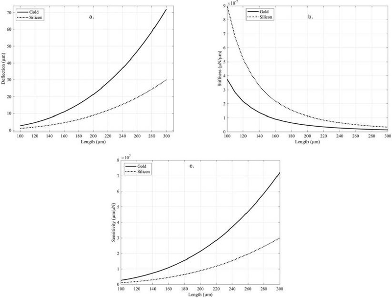
Figure 1 Change in properties with length a. deflection b. stiffness c. sensitivity.
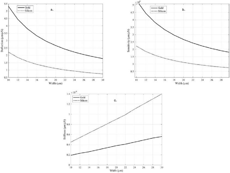
Figure 2 Change in properties with width a. deflection b. stiffness c. sensitivity.
Besides the change in deflection, sensitivity and stiffness of silicon and gold with respect to length and width, the mismatch in these values needs consideration. In comparison to the external factors that cause the failure of the RF MEMS such as environment, electrical etc., the inherent mismatch in mechanical properties of this bimetallic structure is to be considered. With an increase in length as it can be seen from Table 1 the change in the mismatch of deflection increase from 1.556 m for 100 m length to 2.070 m for 110 m length where as for the length of 300 m the mismatch increases up to 42 m. Initially with the increase of 10 m length (from 100 to 110 m) the difference in deflection is only 0.54, but as the length increases to 290–300 m, the change in deflection mismatch for every 10 m is 55.90 m. It is desirable to have the mismatch is these properties to be kept minimum.
4 Conclusion
The deflection mismatch of gold and silicon increases from 1.55 m to 42 m with increase in length from 100 m to 300 m. The defection and sensitivity mismatch between gold increases with increase in length whereas the stiffness decreases with the increase in length. It is also observed that the values of deflection, sensitivity and stiffness with an increase in width is opposite to that of length. It is expected that the stiffness should be sufficient for RF MEMS. RF MEMS is subjected to vibration, shocks and noise. Acceleration of vibration is minimized with the increased stiffness. Balanced stiffness and sensitivity is needed to handle acceleration of resonance which will prevent malfunction and failure due to mechanical fatigue [8] Size optimization plays an important role in minimizing mechanical failures.
References
[1] Xu, Yingyu, Shuibin Liu, Chunhua He, Heng Wu, Lianglun Cheng, Guizhen Yan, and Qinwen Huang. “Reliability of MEMS inertial devices in mechanical and thermal environments: A review.” Heliyon (2024).
[2] Hossain, Nayem, Md Zobair Al Mahmud, Amran Hossain, Md Khaledur Rahman, Md Saiful Islam, Rumana Tasnim, and Md HosneMobarak. “Advances of Materials Science in MEMS Applications: A Review.” Results in Engineering (2024): 102115.
[3] Lysenko, Igor E., Alexey V. Tkachenko, Olga A. Ezhova, Boris G. Konoplev, Eugeny A. Ryndin, and Elena V. Sherova. “The mechanical effects influencing on the design of RF MEMS switches.” Electronics 9, no. 2 (2020): 207.
[4] Kurmendra, and Rajesh Kumar. “Materials selection approaches and fabrication methods in RF MEMS switches.” Journal of Electronic Materials 50, no. 6 (2021): 3149–3168.
[5] RF MEMS switches. Electronics (Switzerland), 9(2), 1–26. https://doi.org/10.3390/electronics9020207.
[6] J.Y. Park, G.H. Kim, K.W. Chung, and J.U. Bu. Sensors Actuators A: Phys., 89(1–2), 88 (2001).
[7] R.K. Bansal. Strength of Material, Laxmi Publications, 8131808149, 2018.
[8] Zhu, H., Pan, J., Tan, S., Huang, G., and Song, M. (2022). Design and simulation of RFMEMS switches with the supporting columns. Energy Reports, 8, 390–396. https://doi.org/10.1016/j.egyr.2022.09.159.
Biographies
Edan Khan is an undergraduate Mechanical Engineering student with a specialization in Mechatronics at Sharda University. His work blends mechanical design, simulation, and automation. He has contributed to a range of projects, including CFD analysis of funnel flows, hybrid vehicle retrofitting, and integrating mechatronic systems into functional designs. He has published a research paper on composite materials and is currently involved in patent work related to innovative engineering solutions. Edan has also explored areas like MEMS, thermofluids, and battery safety. As Vice-Captain of Team Tornado Racing, he contributes to the team’s design efforts and overall coordination.
Sarangapani Kennedy is an Associate Professor in the Department of Mechanical Engineering at Sharda University. With over two decades of experience, his research focuses on advanced materials processing, including spark plasma sintering, ceramic coatings, and intermetallics, contributing to innovations in microstructure-property relationships and mechanical performance enhancement.
Dev Sparsh Sangwan is an undergraduate student in Mechanical Mechatronics Engineering at Sharda University. His academic pursuits lie at the intersection of intelligent design and thermal systems, with notable work on a liquid cooling plate optimized through advanced simulation, fin design study focused on enhanced heat dissipation and an cost effective obstacle detection kit developed for assistive mobility solutions. He blends interests in computational fluid dynamics, embedded systems, and automation to explore innovative engineering solutions. Focused on bridging digital tools with physical design, he is driven by the challenge of transforming theoretical insights into practical, real-world applications.
Journal of Mobile Multimedia, Vol. 21_3&4, 447–454.
doi: 10.13052/jmm1550-4646.21346
© 2025 River Publishers