Dynamic Modeling and Closed-Loop Control of a Tapped Inductor Buck Converter
Siripan Trakuldit and Chanin Bunlaksananusorn*
Faculty of Engineering, King Mongkut’s Institute of Technology Ladkrabang, Bangkok, 10520, Thailand
E-mail: siripan_tkd@hotmail.com; chanin.bu@kmitl.ac.th
*Corresponding Author
Received 24 July 2020; Accepted 10 February 2021; Publication 18 June 2021
Abstract
Modern smart electronic and information technology (IT) devices require a low DC voltage for operation. The low supply voltage is typically provided by a dedicated DCDC converter by stepping down the system’s bus voltage (e.g., 12 V). It is essential that the converter possesses a large voltage step-down gain and, at the same time, operates at high efficiency. A tapped inductor buck converter (TIBC) is a topology that has a potential to meet these requirements. It has a simple circuit structure and high efficiency similar to a buck converter, but can give a larger voltage step-down gain. This paper presents a dynamic modeling and closed-loop control of a TIBC. The state space averaging (SSA) method is adopted for the dynamic modeling to derive small-signal transfer functions of the converter. Based on the duty-cycle-to-output voltage transfer function, a closed-loop control is designed to keep the converter’s output voltage constant. To verify the design, a prototype TIBC with closed-loop control is implemented. Experimental results show that the prototype converter has good output voltage regulation and fast transient response when subject to a step load. The effect of the crossover frequency and phase margin on the converter’s transient response is also illustrated.
Keywords: Tapped inductor buck converters (TIBC), analysis and modeling of DCDC converter.
1 Introduction
Recently, there has been an increasing demand for a DCDC converter with a large voltage step-down ratio. For example, to supply power to integrated circuits (ICs) inside modern smart electronic and information technology (IT) devices, a low voltage, typically ranging from 3.32 V, is used. This low supply voltage is normally obtained from stepping down the system’s bus voltage (e.g. 12 V), using a dedicated DCDC converter known as a load converter. The load converter must be able to perform a wide range of DCDC voltage conversion efficiently. Future ICs will operate on even lower supply voltages, e.g. 1 V or less. Hence, the converter capable of a large voltage step-down is necessary. A conventional step-down DCDC converter is a buck converter [1, 2]. To realize a high step-down ratio, the buck converter would have to operate at an extremely low duty cycle. There are several drawbacks associated with the extreme duty operation [3], such as the malfunction of the main transistor at high switching frequency, the degraded converter efficiency, and the impaired transient response. As a result, some other topologies have been proposed for a high step-down DCDC conversion [4–12]. The quadratic buck converter in [4–6] is essentially two buck converters connected in series but uses only one active switch. Though it has a larger voltage step down ratio than the buck converter, the quadratic converter suffers from higher conduction losses, and, hence, the efficiency is lower than the buck converter. The hybrid buck converters in [7–9] are developed by inserting the L-switching cell or C-switching cell into the conventional buck converter. Their voltage step-down ratio, nonetheless, is only slightly higher than the buck converter, despite the considerable increase in circuit complexity. The tapped inductor buck converter (TIBC) in [10–12] is very attractive due to its simplicity and large voltage step-down capability. The TIBC was developed from the buck converter by replacing a conventional single winding inductor with a two-winding coupled inductor. The voltage gain equation of the TIBC is given by
| (1) |
where v is the output voltage, v is the input voltage, D is the duty cycle, and n is the turn ratio of the coupled inductor. By properly selecting the turn ratio, the voltage step down gain of the TIBC can be made higher than the buck converter, quadratic converter, and hybrid buck converters. Existing publications on the TIBC has mainly focused on steady-state operation and analysis, where the converter works in an open-loop manner. In practical applications, the converter is required to deliver a constant output voltage, although an input voltage and output current may vary. Hence, a feedback control circuit must be incorporated to regulate the output voltage. The steady-state analytical results are only useful for circuit design and component selection but become irrelevant with regard to a closed-loop control design. For the effective closed-loop control design, the converter’s transfer function is needed. This paper presents a dynamic modeling and closed-loop control of a TIBC. The state-space averaging (SSA) method [13, 14] is adopted for the dynamic modeling to derive small-signal transfer functions of the converter. Based on the duty-cycle-to-output voltage transfer function, a closed-loop control is designed to keep the converter’s output voltage constant. The performance of the closed-loop controlled TIBC is validated by experimental results.
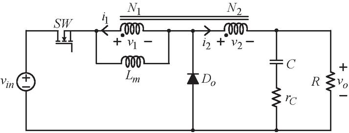
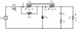
Figure 1 Tapped inductor buck converter.

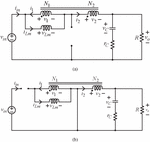
Figure 2 Equivalent circuits of TIBC. (a) SW is turned on. (b) SW is turned off.
2 Modeling of Tapped Inductor Buck Converter
A circuit diagram of the TIBC is shown in Figure 1. The circuit comprises a MOSFET switch (SW), diode (D), capacitor (C), load resistor (R), and coupled inductor. The coupled inductor consists of primary and secondary windings with a number of turns N and N, respectively. The primary and secondary windings are wound on the same magnetic core and connected in series. The connecting point of the two windings called a tap terminal is brought out to the cathode of D. In Figure 1, L is a magnetizing inductance of the coupled inductor and r is the equivalent series resistance (ESR) of the capacitor. The voltage and current relationships of the coupled inductor are similar to those of an ideal transformer, i.e.,
| (2) | ||
| (3) |
where v and v are the primary and secondary voltages, and i and i are the primary and secondary currents. In Continuous Conduction Mode (CCM), the TIBC in Figure 1 has two operating states within one switching cycle.
State 1: When SW is turned on and D turned off, the equivalent circuit is shown in Figure 2(a). Through the circuit analysis, the state-space equations of the converter when the switch is turned on can be written as
| (4) |
where /N and . As seen in Equation (4), the magnetizing current, i, and capacitor voltage, v, are the state variables. The output voltage, v, and input voltage, v, are the output and input variables, respectively.
State 2: When SW is turned off and D turned on, the equivalent circuit is shown in Figure 2(b). Through the circuit analysis, the state-space equations of the converter when the switch is turned off can be written as
| (5) |
Given the state-space equations for the switch-on state in Equation (4) and the switch-off state in (5), the SSA technique [13, 14] can be applied to derive a dynamic model of the converter. The SSA procedure consists of the following steps:
• find the average state-space equations of the converter;
• find the linear small-signal state-space equations of the converter;
• find the transfer functions of the converter.
2.1 Average State-Space Equations of TIBC
The average state-space equations of the TIBC can be found by weigh average of Equations (4) and (5) by the instantaneous duty cycle, d, resulting in
| (6) |
where , , , and are the average magnetizing current, average capacitor voltage, average output voltage, and average input voltage, respectively.
2.2 Linear Small-Signal State-Space Equations of TIBC
The average state-space equations in Equation (6) are a nonlinear continuous-time equation. It can be linearized by small-signal perturbation by substituting , , , , and into Equation (6), where the tilde () symbol represents a small-signal value and the capital letter represents a DC value. Collecting only the small-signal terms and neglecting the product of the two small-signal terms, the linear small-signal state-space equation of the TIBC is obtained as
| (7) |
2.3 Transfer Function of TIBC
The transfer functions of the TIBC can be determined by applying the Laplace transform to the linear small-signal state-space equations in Equation (7). There are six transfer functions that can be derived from Equation (7), but only a duty-cycle-to-output voltage transfer function is needed for feedback control design in Section 3. The duty-cycle-to-output voltage transfer function can be derived as
| (8) |
where
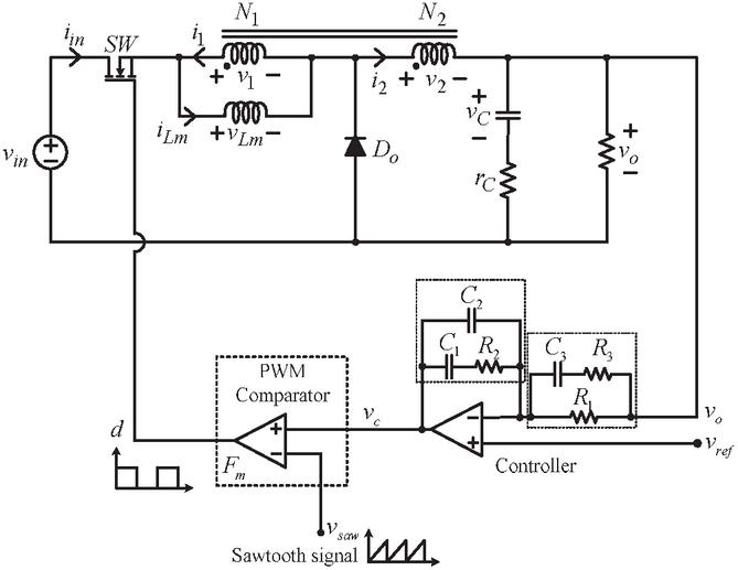
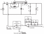
Figure 3 Closed loop controlled TIBC.
3 Closed-Loop Control of TIBC
A closed-loop control of the TIBC is shown in Figure 3. The control circuit consists of a controller and pulse width modulated (PWM) comparator. The converter’s output voltage, v, is fed back to compare with the reference voltage, v. The resulting error voltage is amplified by the controller to generate the control signal, v. At the PWM comparator, v is compared with the constant-frequency sawtooth signal (v). When v is greater than v, the comparator output goes high, and when v is less than v, the comparator output goes low. Hence, the PWM signal is generated at the PWM comparator output, which is used to drive the MOSFET switch. In the literature, the control scheme in Figure 3 is known as Voltage Mode Control (VMC), which regulates the output voltage in the following manner. If v is decreased and lower than v, v will increase. The higher v when compared with the sawtooth signal will cause the duty cycle of the drive signal to increase. As a result, the MOSFET switch will be turned on for longer time duration to increase v. On the other hand, if v is increased and higher than v, v will decrease. The lower v when compared with the sawtooth signal will cause the duty cycle of the drive signal to decrease. As a result, the MOSFET switch will be turned on for shorter time duration to decrease v. In either way, the output voltage will be maintained at the reference value.
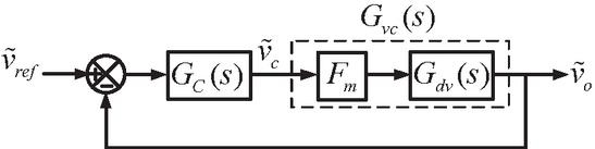
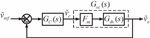
Figure 4 Block diagram of closed-loop controlled TIBC.
The closed-loop control scheme in Figure 3 can be represented in a block diagram form as shown in Figure 4. The TIBC is represented by the duty-cycle-to-output voltage transfer function in Equation (8). Meanwhile, the controller and PWM comparator are represented by the transfer functions G(s) in Equation (9) and F(s) in Equation (10), respectively.
| (9) | ||
| (10) |
where , , , ), , and is a peak amplitude of the sawtooth signal.
From the block diagram in Figure 4, the open-loop transfer can be written as
| (11) |
where . Given the value of V and the TIBC circuit parameters, G(s) can be determined. Once G(s) is known, the controller design can be carried out using the frequency response method [14]. As shown in Equation (9), the controller has two zeros and three poles. These poles and zeros will be placed at appropriate frequencies to compensate the effect of zeros and poles of G(s) so that the resulting open-loop transfer exhibits the desired frequency response. To ensure the stability of the closed-loop control, the open-loop transfer function must have a positive phase margin (PM) and a crossover frequency not exceeding one-tenth of the switching frequency.
4 Controller Design
Circuit parameters of the TIBC are listed in Table 1.
Table 1 Circuit parameters of TIBC
| Parameters | Values |
| v | 48 V |
| v | 5 V |
| R | 1 |
| L | 200 H |
| C | 440 F |
| r | 16.5 m |
| D | 0.32 |
| n | 0.33 |
| V | 1.8 V |
| f | 100 kHz |
With V, V, and , the duty cycle can be calculated from Equation (1), resulting in . The converter is assumed to be operating at the output current of 5A, i.e., . The converter’s switching frequency is 100 kHz. The sawtooth signal has a peak amplitude of V. Based on the parameters in Table 1, the transfer function G(s), which is a product of G(s) in Equation (8) and F(s) in Equation (10), is given by
| (12) |
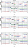
G(s) has the DC gain , the zero at rad/s, the right-half-plane (RHP) zero at rad/s, and the double poles at rad/s. The frequency response of G(s) in Equation (12) is plotted and shown by a dashed line in Figure 5.
Given in Equation (12), the controller design can now be carried out. The controller parameters are selected as follows.
• To compensate the double poles of G(s), the two zeros of G(s) are placed at rad/s and rad/s.
• To compensate the zero and RHP zero of G(s), the poles of G(s) are placed at rad/s and rad/s.
• One remaining pole of G(s) is located at the origin, which is desirable as it helps to increase the DC gain of the open-loop transfer function required for a good output voltage regulation.
• To get the crossover frequency of one-tenth of the switching frequency or 10 kHz, rad/s is selected.
With these selected parameters, the controller’s transfer function becomes
| (13) |
The frequency response of G(s) in Equation (13) is plotted and shown by a dotted line in Figure 5(a). Knowing the parameters , , , , and , the controller’s component values can be calculated, resulting in k, R k, R , C nF, C nF and C nF.
Multiplying Equations (12) and (13), the open-loop transfer function is given as
| (14) |
The frequency response of T(s) in Equation (14) is plotted and shown by a solid line in Figure 5(a). The open-loop transfer function has a high DC gain, a PM of 45, and a crossover frequency of 10 kHz which is one-tenth of the switching frequency.
To study how the crossover frequency (f) and PM affect the performance of the closed-loop controlled TIBC, the controller has been designed and categorized into three different cases as shown in Table 2. The controller in case I is the one whose design was described above, with kHz and PM 45 (Figure 5(a)). The controller in case II has been designed to result in the open loop transfer function with kHz and PM 20 (Figure 5(b)), and the controller in case III with kHz and PM 45 (Figure 5(c)). The effect of the PM on the control performance can be studied using the controller in cases I and II. On the other hand, the effect of the crossover frequency on the control performance can be studied using the controller in cases I and III.
Table 2 Parameters and component values of controller in cases I, II, and III
| I | II | III | |
| (PM 45 | (PM 20 | (PM 45 | |
| Cases\Values | kHz) | kHz) | kHz) |
| 5.62 10 rad/s | 5.74 10 rad/s | 2.57 10 rad/s | |
| 7.85 10 rad/s | 7.85 10 rad/s | 7.85 10 rad/s | |
| 9.42 10 rad/s | 8.17 10 rad/s | 8.17 10 rad/s | |
| 1.89 10 rad/s | 1.10 10 rad/s | 1.13 10 rad/s | |
| 4.27 10 rad/s | 1.48 10 rad/s | 5.59 10 rad/s | |
| 3.2 k | 3 k | 6.8 k | |
| 2.4 k | 2.4 k | 2.4 k | |
| 73 | 179 | 101 | |
| 53 nF | 53 nF | 53 nF | |
| 2.3 nF | 4 nF | 4 nF | |
| 32 nF | 38 nF | 18 nF |
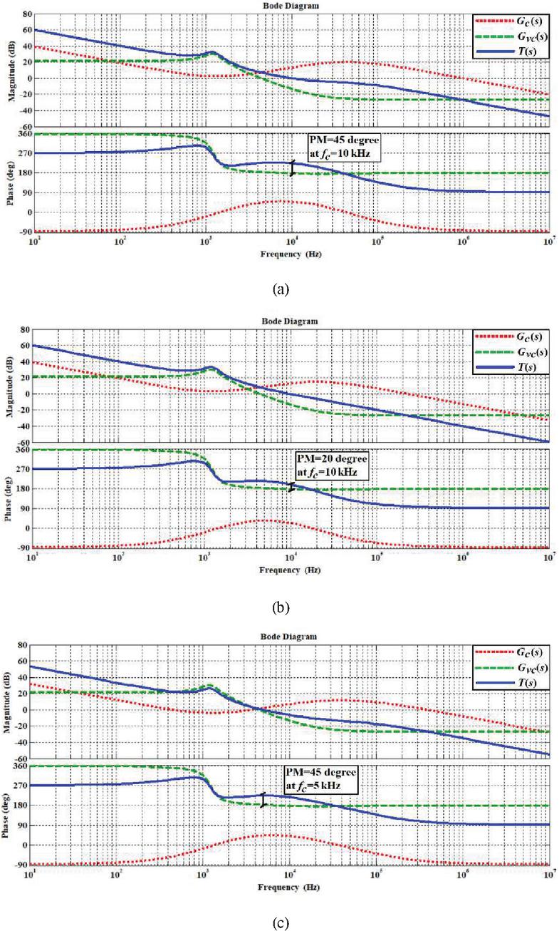
Figure 5 Frequency responses of , , and for controller in (a) Case I, (b) Case II, and (c) Case III.
5 Experimental Results
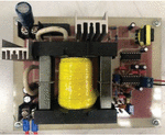
Figure 6 shows a prototype closed-loop controlled TIBC. The circuit parameters are the same as those listed in Table 1. Operated at a switching frequency of 100 kHz, the prototype circuit converts the input voltage V into the output voltage V, and can supply the output current from 1 to 5 A. The output voltage is regulated via a feedback control scheme shown in Figure 3. On the prototype circuit board, the controller components, i.e., and , can be removable, allowing the different controllers in Table 2 to be used for experiment.
Table 3 shows the output voltage measured from the prototype circuit at different output currents. It can be seen that the output voltage is maintained closed to 5 V throughout the output current range. A high precision digital voltmeter was used in this measurement and the same value of output voltage was recorded for each controller case. Since there is no distinction in the measured results, it is concluded that the three controllers perform equally well with regard to the steady-state output voltage regulation. All the controllers in cases I, II, and III are able to deliver a tight steady-state output voltage regulation due to the pole at the origin, which has contributed to the high DC gain of the open-loop transfer function. Referring to Figure 4, the closed-loop transfer function, T(s), can be expressed in terms of the open-loop transfer function, T(s), as
| (15) |

Figure 6 TIBC prototype circuit.
Table 3 Output voltage measured from prototype converter
| (V) | |||||
| Controller | A | A | A | A | A |
| Case I | 5.000 | 4.998 | 4.995 | 4.993 | 4.991 |
| Case II | 5.000 | 4.998 | 4.995 | 4.993 | 4.991 |
| Case III | 5.000 | 4.998 | 4.995 | 4.993 | 4.991 |
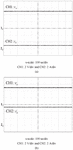
At DC or steady-state condition, the high gain open-loop transfer function, i.e., large T(s), would result in the unity gain closed-loop transfer function, i.e., . The unity closed-loop gain implies that the output voltage would closely follow or track the reference value. This explains why the prototype TIBC employing the controllers in cases IIII all exhibits a good regulation characteristic. Figure 7 shows a sample of the output voltage and current measured by the digital oscilloscope, whereby the output voltage appears to be at about 5 V for the 1 and 5 A output currents.
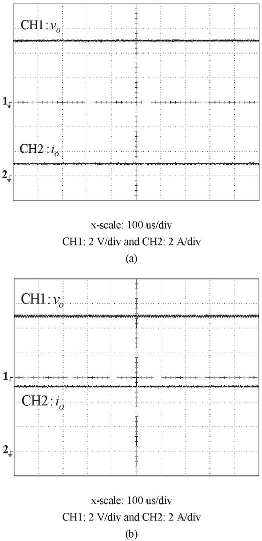
Figure 7 Output voltage waveform measured from the prototype TIBC at (a) A and (b) A.
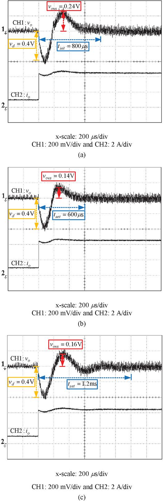
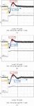
Figure 8 Output voltage transient response due to a step load for controller in (a) case I, (b) case II, and (c) case III.
Next, the dynamic performance of the closed-loop controlled TIBC is investigated. A step load change is applied to the prototype converter, which causes the output current to suddenly increase from 1 to 5 A. The output voltage responses due to the step load are shown in Figure 8. The abrupt increase in the output current causes the output voltage to drop momentarily. In all cases, the controllers are able to restore the output voltage back to 5 V by the regulation mechanism described in Section 3. Nonetheless, the output voltage transient characteristics are different for each case of controller. As seen by comparing Figure 8(a) and 8(b), when the PM is reduced from 45 to 20 and the crossover frequency remains unchanged at 10 kHz, the output voltage response has been dampened, resulting in the improved transient performance. That is, the voltage overshoot has reduced from V in Figure 8(a) to V in Figure 8(b), and the settling time reduced from s in Figure 8(a) to s in Figure 8(b). As seen by comparing Figure 8(a) and 8(c), when the crossover frequency is reduced from 10 to 5 kHz and the phase margin remains unchanged, the output voltage has become less responsive. That is, the settling time has increased from s in Figure 8(a) to ms in Figure 8(b). In all cases, the maximum transient voltage drop is the same, i.e., V. Comparing among the responses in Figure 8, it is evident that the controller in case II yields the optimal transient performance.
6 Conclusion
This paper has presented a dynamic modeling and closed-loop control of a TIBC. The SSA method was adopted to derive small-signal transfer functions of the converter. Based on the derived duty-cycle-to-output voltage transfer function, the controller was designed using the frequency response method to keep the output voltage constant. The controller design essentially involved placement of its poles and zeros to shape the converter’s open-loop transfer function to attain the desired frequency response, which includes a high DC gain, a positive phase margin, and a crossover frequency not exceeding onetenth of the switching frequency. As such, three cases of the controller, which give different values of the PM and crossover frequency, were designed as shown in Table 2. Experimental results obtained from the prototype converter showed that the good steady-state output voltage regulation is achieved by all the three controllers. This is attributed to the pole at the origin of the controller which yields the open-loop transfer function with a high DC gain. As for the converter transient performance, the control in case II provided the best result as it gives the shortest settling time (t) and lowest voltage overshoot (v) as shown in Figure 8. The effect of the PM and crossover frequency on the converter’s transient performance was also studied. It was revealed that the transient response can be dampened by lowering the PM and made less responsive by lowering the crossover frequency.
Acknowledgment
This work is supported by Faculty of Engineering, King Mongkut’s Institute of Technology Ladkrabang (contract number 2563-02-01-031).
References
[1] D. W. Hart, Power Electronics, McGraw-Hill Companies, 2011.
[2] A. I. Pressman, K. Billings, and T. Morey, Switching Power Supply Design, 3rd ed., McGraw-Hill Companies, 2009.
[3] Y. Jiao and F. L. Luo, “N-switched-capacitor buck converter: topologies and analysis”, IET Power Electronics, Vol. 4, Issue 3, 2011, pp. 332–341.
[4] D. Maksimovic and S. Cuk, “Switching converters with wide DC conversion range”, IEEE Transactions on Power Electronics, Vol. 6, Issue 1, 1991, pp. 151–157.
[5] M.G. Ortiz-Lopez, J. Leyva-Ramos, E.E. Carbajal-Gutierrez, and J.A. Morales-Saldana, “Modelling and analysis of switch-mode cascade converters with a single active switch”, IET Power Electronics, Vol. 1, No. 4, 2008, pp. 478–487.
[6] A. Agasthya and M. K. Kazimierczuk, “Steady-state analysis of PWM quadratic buck converter in CCM”, IEEE 56th International Midwest Symposium on Circuits and Systems, 2013, pp. 49–52.
[7] B. Axelrod, Y. Berkovich, and A. Ioinovici, “Switched-capacitor/switched-Inductor structures for getting transformerless hybrid DC–DC PWM converters”, IEEE Transactions on Circuits and Systems, Vol. 55, Issue 2, 2008, pp. 687–696.
[8] B. Axelrod, Y. Berkovich, S. Tapuchi, and A. Ioinovici, “Single-stage single-switch switched-capacitor buck/buck-boost-type converter”, IEEE Transactions on Aerospace and Electronic Systems, Vol. 45, Issue 2, 2009, pp. 419–430.
[9] O. Pelan, N. Muntean, and O. Cornea, “Comparative evaluation of buck and switched-capacitor hybrid buck DC-DC converters”, International Symposium on Power Electronics, Electrical Drives, Automation and Motion, 2012, pp. 1330–1335.
[10] K. Yao, M. Ye, M. Xu, and F.C. Lee, “Tapped-inductor buck converter for high-step-down DC-DC conversion”, IEEE Transactions on Power Electronics, Vol. 20, Issue 4, 2005, pp. 775–780.
[11] K. W. E Cheng, “Tapped inductor for switched-mode power converters”, International Conference on Power Electronics Systems and Applications, 2006, pp. 14–20.
[12] C. Ankit, A. Ayachit, D. K. Saini, and M. K. Kazimierczuk, “Steady-state analysis of PWM tapped-inductor buck DC-DC converter in CCM”, IEEE Texas Power and Energy Conference, 2018, pp. 1–6.
[13] E. Vuthchhay and C. Bunlaksananusorn, “Dynamic modeling of a zeta converter with state-space averaging technique”, International Conference on Electrical Engineering/Electronics, Computer, Telecommunications and Information Technology, 2008, pp. 969–972.
[14] E. Vuthchhay and C. Bunlaksananusorn, “Modeling and control of a zeta converter”, International Power Electronics Conference, 2010, pp. 612–619.
Biographies

Siripan Trakuldit received the B. Eng. degree in electrical engineering from Walailak university and M. Eng. degree in control engineering from King Mongkut’s Institute of Technology Ladkrabang (KMITL), Thailand, in 2008 and 2012, respectively. Her research interest is power electronics.

Chanin Bunlaksananusorn received a Ph.D. degree in electrical engineering from The University of Edinburgh, UK, in 1997. He is currently an associate professor with the Faculty of Engineering, King Mongkut’s Institute of Technology Ladkrabang (KMITL). His research interests are power electronics and energy conversion.
Journal of Mobile Multimedia, Vol. 17_4, 673–692.
doi: 10.13052/jmm1550-4646.1749
© 2021 River Publishers