Novel MAGFinFET: Operation, Design and Geometry Effect for Modern Sensors
Khine Thandar Nyunt Swe1, Chanvit Pamonchom1, Amporn Poyai2 and Toempong Phetchakul1,*
1Department of Electronics, School of Engineering, King Mongkut’s Institute of Technology Ladkrabang, Bangkok, Thailand
2Design & Engineering Consulting Service Center (DECC), National Science and Technology Development Agency (NSTDA), Thailand
E-mail: 64601006@kmitl.ac.th; 58601325@kmitl.ac.th; amporn.poyai@nectec.or.th; toempong.ph@kmitl.ac.th
*Corresponding Author
Received 25 October 2021; Accepted 29 January 2022; Publication 17 March 2022
Abstract
This paper presents a new magnetic detection device, MAGFinFET, which is based on the advanced 3D FinFET structure. It can measure the vertical magnetic field by designing two contacts on both sides of the drain. The operation uses the principle of the current mode of Hall effect causing the deflection of the drain currents at both contacts. The 3D geometry effect was studied: channel length, fin height and fin width. It can be seen that when the values of these parameters are increased, the differential currents and relative sensitivities are increased linearly. Relative sensitivity has the highest value 0.00201 T at channel length 50 nm. Fin height and fin width of 50 nm give the highest sensitivity of 0.00468 T and 0.00415 T respectively. Current density distributions of the different variations of each parameter L, F and F are observed by applying vertical magnetic field on the device. The 3D-MAGFinFET has been compared to that of the 2D non-split drain MAGFET structure and bulk fin resistor that use n-type semiconductor instead of induction channel. MAGFinFET shows quite higher sensitivity compared to bulk fin resistor. MAGFinFET mechanism models and simple characteristic equations are proposed in this work. Sentaurus TCAD is used for the device structure and simulation for the characteristics of MAGFinFET. This FinFET based device can be fabricated with modern integrated circuit technology.
Keywords: MAGFinFET, FinFET, MAGFET, Lorentz’s force, TCAD.
1 Introduction
Today technology works everything with the help of sensors, controllers and actuators. Intelligent Transportation System (ITS), smart healthcare system, smart farm, smart home, robotic and automation use various kinds of sensors to monitor and control their systems and appliances. Magnetic sensors are the sensors that detect magnetic field and have been widely used in various applications such as Internet of Things (IoT), Surveillance systems, Automotive systems, Artificial Intelligence (AI), space technology, Data storage system like Static Random Access Memory (SRAM) and others [1–4]. Magnetic sensors or detectors can be used for magnetic data communication. In magneto inductive communication, high sensitivity magnetic detectors can be used on the receiver side. Different kinds of magnetic sensor can detect different range of magnetic field. Among all others, Hall sensors are popular and reliable for magnetic communication [5]. For the traffic flow and vehicle classification, wireless magnetic sensor networks are used at the intersections and in free ways with 80 percent accuracy rate of classification [6–8]. In the age of mobile multimedia age, people rely on mobile phone that has many embedded sensors like accelerometer, gyro and others. Smart health care system is built on the multimedia application with the help of the embedded sensors of mobile phone [9].
There are various kinds of magnetic sensors that detect magnetic field. Hall sensors are used as contactless current sensor, biosensor and compass. Silicon based Hall sensor is compatible with CMOS technology. However, it still has challenges to detect small signal and amplify the signals [10]. Hall sensors fabricated with CMOS technology that is based on Hall plate has low sensitivity and vulnerable to process fluctuation, temperature drift and package induced stress [11–13].
The conventional MOSFET was used as magnetic sensor known as Magnetic FET (MAGFET). MAGFET is a magnetic field sensor device based on a MOSFET planar structure. MOSFET planar structure is considered for the reason that MOSFET is the most fundamental and most important basic element in Integrated Circuits (ICs). The conventional MAGFET structure is a MOSFET structure with two symmetrical split drains.
In Hall effect, there are two modes of operation that are voltage mode and current mode. In this paper, current mode of Hall effect is considered for the detection of magnetic field. The operation of MAGFET is based on the principle of deflection of the current induced by the magnetic field perpendicular to the surface of the device, causing a linear difference in the current according to the intensity and direction of the magnetic field [14–16].
However, modern technology markets demand for nano-scale devices for the compact design and low power consumption products. Therefore, scaling process on the semiconductor devices plays an essential role to integrate more and more transistors in one integrated circuit in every technology node. Due to the advancement of integrated circuit technology and its application requirements, the size of the MOSFET is steadily becoming smaller, according to the Moore’s law, the number of transistors per area doubles every two years, nanometer level at present time. It needs continuous reduction in the transistor size. In the conventional MOSFET structure (2D planar technology), channel length at sub 10 nm causes leakage current and the undesired short channel effects. To solve that issue, Metal Oxide Semiconductor Field Effect Transistor (MOSFET) had the significant success in the three-dimensional structure [17]. The conducting channel was wrapped by the gate electrodes. That kind of transistor structure that has fin like conduction channel is called FinFET. This device structure helps to reduce Drain Induced Barrier Lowering (DIBL) effect and the leakage current [18, 19]. This structure allows one to scale the channel length down independently from other scaling parameters. Intel introduced this technology in microprocessors in 2011 [20]. Based on the concept of MAGFET, the idea of 3D FinFET structure and applying magnetic field are designed to be Magnetic FinFET (MAGFinFET) in nano meter scale [21].
By using FinFET technology, it reduces the problems of short channel effect, drain induced barrier lowering, high leakage current. Scaling down to sub 10 nm channel length becomes possible. The MAGFinFET uses the principle of operation to deflect the current from the force induced by the vertical magnetic field. The function and characteristics of MAGFinFET shows the similar results of the conventional MAGFET. By adding special design concept of current mode device, the MAGFinFET is possible to detect the magnetic field in the vertical direction perpendicular to device. By using TCAD Sentaurus simulation, an operation, design and the effect of the geometric parameters of the structure which are channel length, fin height and fin width have been studied in this work.
2 Concept and Fundamental of MAGFinFET
2.1 MAGFET
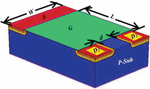
MAGFET is a device used to detect a magnetic field with the basic structure of MOSFET device. The structure of MAGFET is shown in Figure 1. The structure is a MOSFET composed of two separate drains D and D, a gate G and a source S, so called, split drain MOSFET. Magnetic field can deflect the charge in the semiconductors. Effect of magnetic field on the device can be detected by measuring Hall voltage or Hall current. In this MAGFET device structure, Hall current that occurs according to the unbalanced drain currents in split drain contacts is used to calculate the sensitivity of the device [22]. The sensitivity can be varied depending on the conditions such as the distance between two drains, mobility of the carriers in the channel and the aspect ratio of MAGFET [15, 23].

Figure 1 Split drain MAGFET structure.
When there is no perpendicular magnetic field applied to the device, the values of the two drain currents are equal ideally. When magnetic field is applied, the currents are deflected according to direction and intensity of magnetic field. Those deflecting drain currents occur in the current mode of Hall effect. The divergence of the current causes the drain current to lose equilibrium, causing the difference in the currents. The current difference I is defined as
| (1) |
The current difference is equal to Hall current and can be written as follow [24]
| (2) |
where I is Hall current, is channel mobility, L is length of channel, W is width of channel, G is geometrical correction factor of device, is total biased drain current and B is applied magnetic field perpendicular to device. The relative sensitivity of device is defined as
| (3) |
The maximum relative sensitivity S is given by
| (4) |
Although the L/W is approaching infinity, the current deflection condition occurs in a short Hall structure so that the Hall voltage cannot completely offset the Lorentz force. Therefore, this ratio is the ratio at which the resulting device length should have a narrow width value to get better sensitivity.
2.2 Gapless Design MAGFET (Non-split Drain MAGFET)
From the afore mentioned MAGFET working principle, the drain is symmetrically divided into two halves, for the purpose of supporting the difference current I arising from the magnetic induction force defeated by the Hall electrical force. Therefore, the sensitivity in Equation (3) assumes that the gap between the drains should be as small as possible which will give geometrical correction factor G close to 1. It is the condition to get the highest sensitivity.
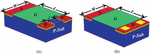
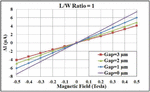
However, firstly the researcher proposed a MAGFET design that does separate the two drains, instead of separating the contacts in one drain for supporting current difference I. It is called non-split drain MAGFET which the structure of device comparing to conventional MAGFET is shown in Figure 2. Figure 2(a) is conventional split drain MOSFET structure and Figure 2(b) is non-split drain MOSFET with split contact in a drain. Figure 3 is differential current and magnetic field density characteristics of MAGFET at , biasing current 1 mA, and varied gap between two drains are 0, 1, 2, 3 m [14].
It has been described that the higher sensitivity is, the less gap it is. Non-split drain structure with gap 0 has the highest sensitivity. The experiment results with other aspect ratios also gave the same results. Therefore, it was proved that the gap design between split drain is not necessary for current difference resulting from current deflection [25]. The current continuously deflects from the channel into the drain and flow out at the nearest contacts in drain which reduces the losses arising from discontinuity from the gap. This design is independent from limitation of fabrication technology.
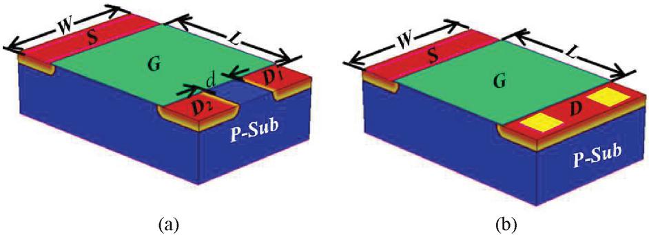
Figure 2 Comparison of MAGFET structures (a) conventional split drain structure (b) non-split drain structure.
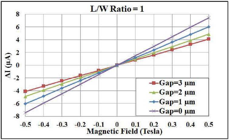
Figure 3 Differential current-magnetic field characteristic responses of MAGFET.
2.3 FinFET
MOSFET devices are the basic elements of integrated circuits. Due to the demands of various applications, there is a need to reduce or scaling the device down, making the cost significantly lower. Moreover, the smaller device has an increased current density, requiring lower voltage and lower power consumption and higher speed. From the very beginning of the first integrated circuit to the present, the size of MOSFET has steadily decreased, which is now at the nanometer scale.
Figure 4 FinFET structure.
However, Short Channel Effect (SCE) arises in reducing the size of MOSFET. The subthreshold current problem, which is the current flowing while the gate voltage is less than the threshold voltage , plays a greater role as the MOSFET becomes smaller. At and , this current is called off current (I) will increase and V rolled off as a result of Drain Induced Barrier Lowering (DIBL). I will increase as the threshold voltage decreases. In order not to reduce the threshold voltage, it is necessary to do other scaling, such as thinner oxide thickness, shallower drain and source junction, and greater substrate concentration [26]. In the latter case, the mobility value decreased by impurity scattering, causing the current density to decrease, the on current I is decreased. In addition, the thickness of the substrate has an effect on the bulk leakage current under the channel.
To eliminate all of the above problems, it is necessary to have a new structure to replace the traditional MOSFET structure. The FinFET structure became the solution to reduce the short channel effect. The structure of FinFET is shown in Figure 4 and it resembles a fish fin with a three-dimensional (3D) structure. From the structure showing the drain, source and double gate, the important geometry parameters are channel length L, fin height F and fin width F. From the structure, the thickness of the substrate is the width of the fin F itself. In FinFET structure, gate is wrapped around the channel. This structure is appropriate for application in memory cells because of properties like reduction in channel leakage current and switching time, this structure also grants better electrostatic control on channel [27]. Therefore, the leakage current under the base plate is greatly reduced, the channel dopant concentration is not required to be concentrated, and the mobility is higher. The double channel allows for a higher current density. The channel scaling is independent from other mentioned parameters; it can be reduced in the order of several nanometers. Currently, FinFET has been scaled down to 14 nm FinFET and it is used for enhancing graphic card, boosting game system and interactive multimedia demands [28, 29].
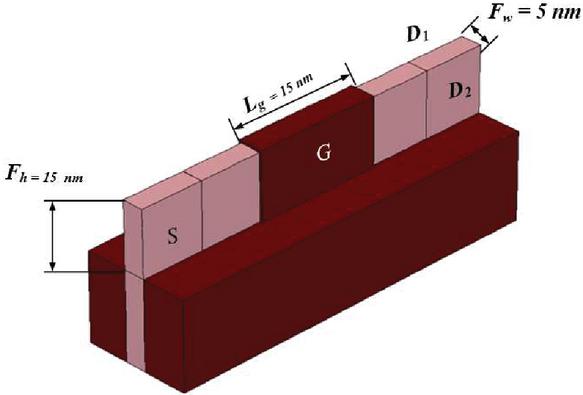
Figure 5 MAGFinFET structure.
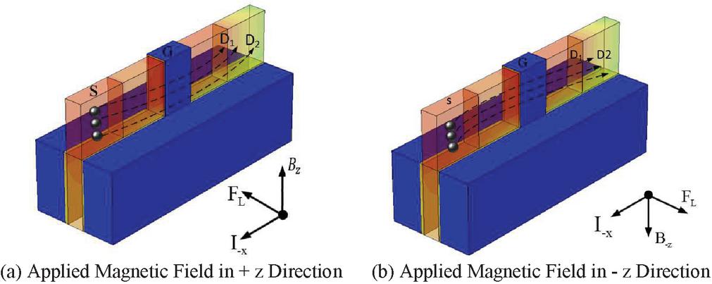
Figure 6 MAGFinFET mechanism models.
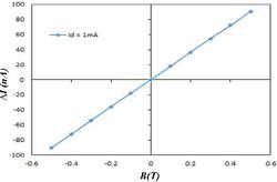
Figure 7 Transfer characteristics of MAGFinFET.
2.4 MAGFinFET
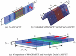
MOSFET has developed to FinFET structure in integrated circuit technology. The MAGFET device is based on a MOSFET structure, and has the advantage that it can be built with MOSFET in an integrated circuit. FinFET structure has not been used as magnetic field detecting device. This idea of using FinFET as magnetic field detecting device came from the non-split drain MAGFET design concept. That FinFET structure is called MAGFinFET. The structure of the device is shown in Figure 5. The structure consists of a fin with a drain, double gate and source like a conventional FinFET. The difference is that its drain has two contacts on the left and right sides of the fin, D and D.
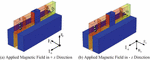
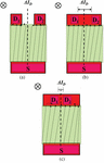
This design can be compared to a planar non-split drain design, where the two contacts of the drain act to receive the current difference caused by current deflection due to the Lorentz’s force induced by the intensity and direction of the magnetic field in the vertical direction. MAGFinFET operates by applying biased voltage at the gate and drain, the drain currents I and I are equal when no magnetic field is applied. When the magnetic field is applied in the z direction, the Lorentz force is induced in the y direction and causes the two drain currents to become unbalanced, deflecting them to D. This phenomenon causes I greater than I as shown in Figure 6(a). Likewise, while giving a magnetic field in the -z direction, the Lorentz’s force acts on the electron current in the -y direction, causing I greater than I. Figure 6 shows the mechanism models of MAGFinFET when magnetic field is applied perpendicular to the channel of the device. The magnetic characteristic of MAGFinFET is shown in Figure 7 [21] where the differential current is linearly related to the intensity and direction of the magnetic field.
3 Device Structures and TCAD
3.1 Device Structure
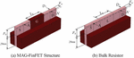
Geometrical parameters of the device structure have impact on detecting the magnetic field. In this study, the effect of the device’s geometrical parameters on detecting magnetic fields is figured out by changing their values. These variables are channel length (L), fin width (F) and fin height (F). The device structure is shown in Figure 8(a) consisting of drain, gate and source. There are two contacts in both sides of drain D and D. Gate has three surfaces of metal that are top, left surface and right surface.

Figure 8 Device structures.
There are some parts of the fin structure deep below the oxide depending on the device processing technology. The fin material is silicon with an n type dopant concentration in the drains and source 10 cm. Boron and phosphorus dopants are used for p type and n type. The channel is intrinsic silicon with the concentration 10 cm. The oxide material is SiO with the thickness of 0.5 nm. The parameters of the FinFET structure such as L, F and F are varied at 10, 20, 30, 40 and 50 nm.
In addition, a comparative study was performed between the MAGFinFET structure and the fin resistor. The structure of fin resistor is shown in Figure 8(b). The structure in Figure 8(b) does not have double gate induced channel, but it uses as an n-type semiconductor with a dopant concentration of 10 cm. It is the difference between FinFET and fin resistor. This structure is fin resistor with drain contacts (D and D) and source as electrodes. The device structures of FinFET and bulk resistor are created by using the structure editor of Sentaurus TCAD. The structures are meshed before the physical and mathematical calculations to analyse on the electrical and magnetic characteristics of the device.
3.2 TCAD
This study used TCAD simulation in the study. Sentaurus TCAD is a well-known professional program for nano/micro fabrication process and device simulation [30–32]. Shockley Read Hall (SRH) model is used for recombination. There are important key models that are completely involved within this program. In addition to electrical simulations, there are other models involving light, heat, stress and strain, as well as magnetic fields. The relevant magnetic field models are shown as follows
where is n or p type semiconductor, is carrier current density vector, is current vector without mobility, is the Hall mobility, is the magnetic induction vector and B is the magnitude of vector.
4 Simulation Results and Discussion
The electrical properties of the FinFET device were examined firstly. The current-voltage characteristic is shown in Figure 9. Drain and gate voltage (V and V) which is incremented by 0.2, has a maximum value of 1 V. This electrical characteristic curve shows that it has similar characteristics like MOSFET.
Figure 10 is the plot between the drain current and the gate voltage. The drain voltage is kept constant at 1 V, while the gate voltage is increased from 0 to 1 V with 0.2 V step each time. Vertical axis is the drain current in log scale and the horizontal axis V is in linear scale. The threshold voltage V is obtained from the gate voltage at which the drain current is 100(nA)(W/L). The lowest threshold voltage value 0.15 V is obtained at nm while other , 30, 40 and 50 nm give approximately 0.2–0.22 V. I is the drain current at which is maximum supply voltage and I is drain current at which and is 0 V. From Figure 10, it can be seen that the I at all channel lengths will have the same value for 4.29 A. I can be separated in two groups: nm and the other channel lengths. current at length nm is 0.82 nA and at any other length are in the range of 0.019 to 0.006 nA. Off current increases as becomes lower. Subthreshold swing values are reasonable values 63 mV/dec except for channel length nm. According to the electrical characteristics, it can be noted that the nm has some degrading effect on the device. It can be seen clearly in Figure 10.
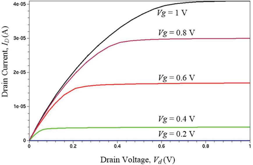
Figure 9 Current-voltage characteristic of MAG-FinFET ( nm).
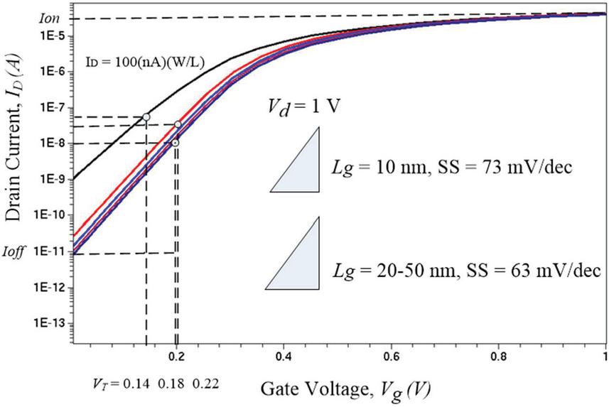
Figure 10 Electrical characteristics of MAGFinFET.
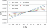
The study of the channel length, L, affecting the magnetic field response was done by applying the perpendicular magnetic field to the device of different channel lengths. The device is biased at a constant current of 100 A, which is A. Constant current bias causes the difference in current () to be caused by current deflection, not by other modulation of magnetic fields. The magnetic field intensity varied from 0–0.5 T in z and – z direction with 0.1 step each time. The magnetic response results were shown in Figure 11 for various values of channel length, while the fin height and width were constant at 15 and 5 nm, respectively. It can be seen that when magnetic field is applied in z direction, drain current is greater than drain current and current difference is positive. When magnetic field is applied in – z direction, current difference is negative. The cases of varied channel length also give the same result. The relative sensitivity that is the absolute sensitivity divided by biasing current, , of channel length 10, 20, 30, 40 and 50 nm are 0.00182, 0.00186, 0.00190, 0.00197 and 0.00201 T, respectively. The sensitivity increases as the channel length increases and tends to be a linear relation.
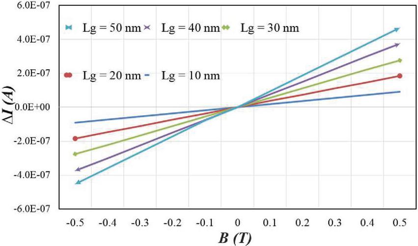
Figure 11 Magnetic responses of MAGFinFET, A.
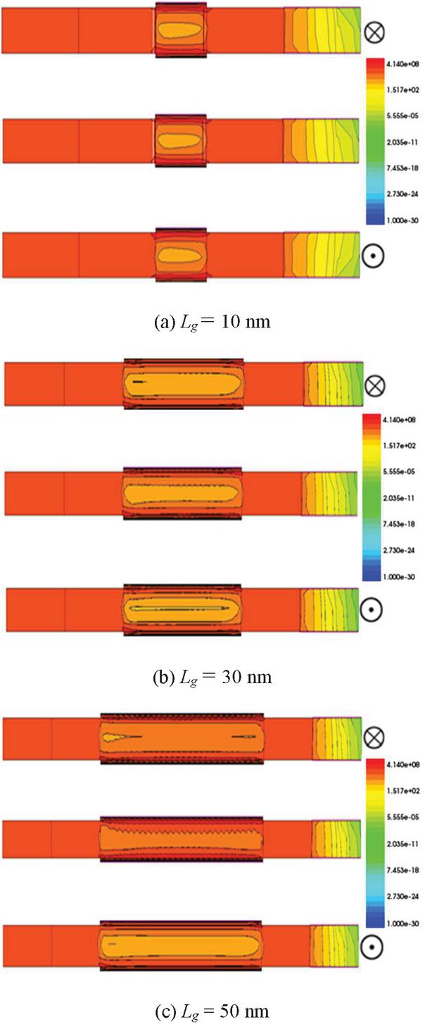
Figure 12 Top view of current density distribution of MAGFinFET at various B 0.5 T, A.
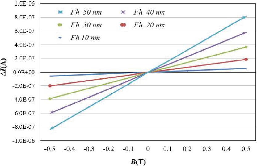
Figure 13 Magnetic response MAGFinFET at various , T, A.
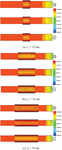
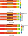
The distribution of current density when receiving a magnetic field of different directions has been compared to when it is not receiving a magnetic field is shown in Figure 12. Figure 12 shows top view of the cross-section A-A of Figure 8. Figures 12(a), (b) and (c) are the examples of short, medium and long channel lengths that were selected, 10, 30 and 50 nm respectively. For each channel length, the middle figure is the case where the magnetic field is not applied, and the figure above and below are the case with applied magnetic field 0.5 T in the direction z and z respectively.
The change was most noticeable in the area under the gate, in the double side channel, and in the middle space charge region. Another area where the change can be observed is in the drain region with contact on both sides. In addition, changes in current density can be observed at longer channels more than at shorter channels. The difference in current density distribution can be hardly seen in the case of 10 nm channel length. Non uniform current density distribution happens more in long channel cross section of drain region rather than that of short channel cross section.
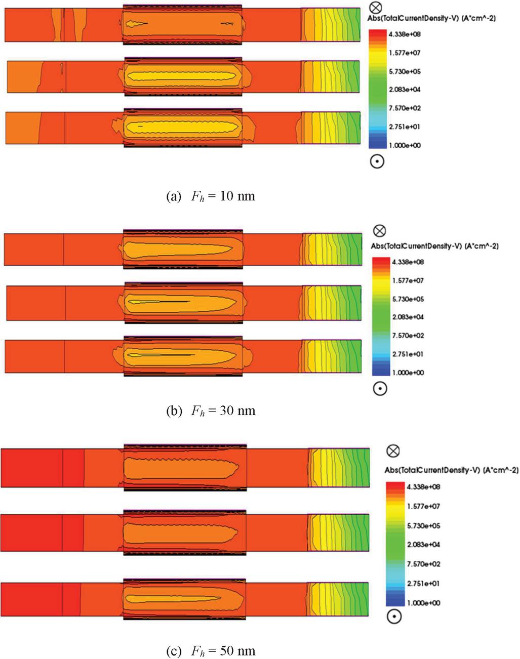
Figure 14 Top view of current density distribution of MAGFinFET at various , B = 0.5 T, A.
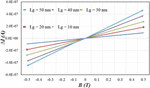
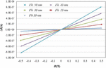
The effect of variations in the fin height F of MAGFinFET structure is studied. The effect of variations of fin height on the magnetic response is shown in Figure 13. The simulation conditions are the same as those in Figure 11. The fin height F was varied at 10, 20, 30, 40 and 50 nm. The values of the fin width F and channel length L were kept constant at 5 and 30 nm respectively. Magnetic field is applied vertically. According to the direction and intensity of magnetic field, the values of current difference are changing. It can be seen that and B characteristics are linearly at all fin height in Figure 13. The relative sensitivities S were 0.00106, 0.00277, 0.00396, 0.00437 and 0.00468 T at the 10, 20, 30, 40 and 50 nm fin heights respectively. The sensitivity increases with the increase in fin height and tends to be a linear increase.
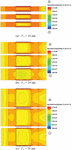
The current density distribution at the various fin heights is shown in Figure 14. Figure 14 is the top view of the cross-section A-A that was described in Figure 8. The cross-section A-A of using minimum fin height 10 nm, medium fin height 30 nm and maximum fin height 50 nm are shown in Figure 14(a), (b), and (c).
The middle figure of each cross-section shows the current density distribution when no magnetic field is applied. The upper figure shows the current density distribution when the value of magnetic field 0.5 T is applied in – z direction. The bottom figure is the cross section that shows the current density when the intensity of magnetic field 0.5 T is applied in z direction. The difference in current density can be clearly seen at different magnetic fields. The area most noticeable for the change is the channel under the gate.
In all the figures obtained by using different fin heights, the current density distribution near the drain contacts looks similar and is difficult to compare the changes in each fin height. The value of current density distribution along the channel is increased when high fin height is used. It can be seen that the current density distribution of source region is also increased at fin height 30 nm and 50 nm compared to the current density distribution at fin height 10 nm. The current density distribution of the channel is the highest at 50 nm fin height.
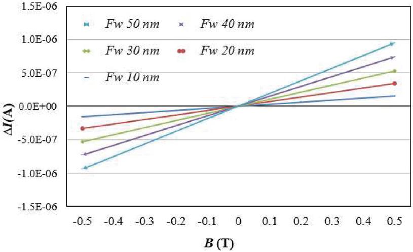
Figure 15 Magnetic response MAGFinFET at various , T, A.
The effect of the fin width F on the magnetic response is shown in Figure 15. The simulation conditions are the same as those in Figure 11. The fin width F varied at 10, 20, 30, 40 and 50 nm, while the values of fin height F and channel length L were kept constant at 15 and 30 nm respectively. and B characteristics are related linearly at all fin width. The relative sensitivities that obtained by using those geometric parameters were 0.00310, 0.00364, 0.00386, 0.00409 and 0.00415 T at the fin widths of 10, 20, 30, 40 and 50 nm respectively. The sensitivity increases as the fin width increases and tends to have a linear increase.
The current density distributions at the various fin widths are shown in Figure 16. Figure 16 is the top view of the cross-section A-A in Figure 8. It shows the changes in current density distributions at a minimum width of 10 nm, a medium width of 30 nm, and a maximum width of 50 nm, as shown in Figure 16(a), (b) and (c) respectively. Effect of magnetic field also changes current density distribution of MAGFinFET device.
The figure in the middle is when it is not receiving a magnetic field. The upper and lower figures show 0.5 T of the magnetic field in – z direction and z direction respectively. The difference in current density can be clearly seen at different magnetic fields. The area most noticeable for the change is the channel under the gate. As the width is wider, the current density changes can be observed in the drains and source as well.
In this work, 3D MAGFinFET structure was introduced and the values of parameters are changed to figure out the differential currents, relative sensitivities and current density distribution by applying magnetic field and supply current. The FinFET structure is changed into bulk fin resistor and its current difference and relative sensitivities are compared to that of MAGFinFET structure. The operation of the MAGFinFET structure uses the deflecting currents in double side channels and the middle space charge in fin region. This kind of the current flow can be made into a bulk fin resistor structure to find out the current difference.
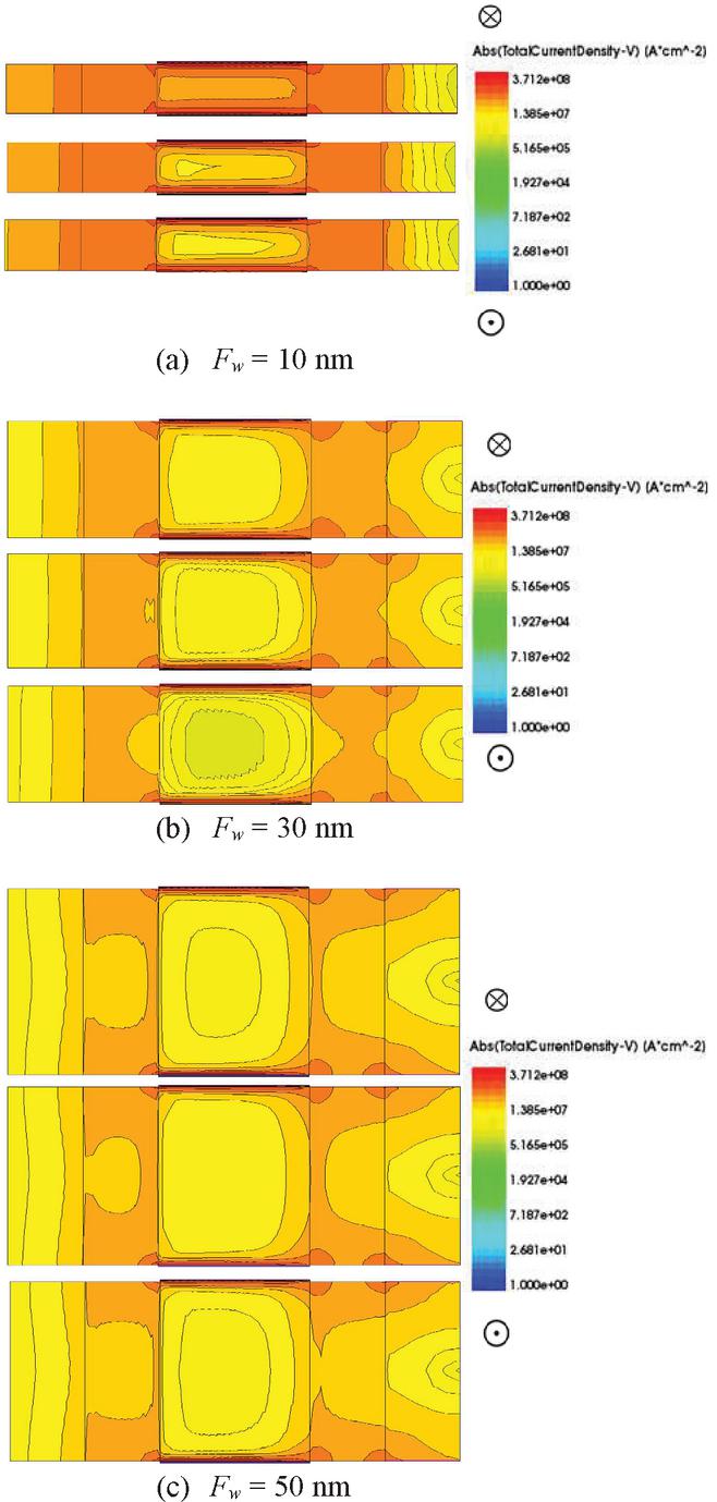
Figure 16 Top view of current density distribution of MAGFinFET at various , T, A.
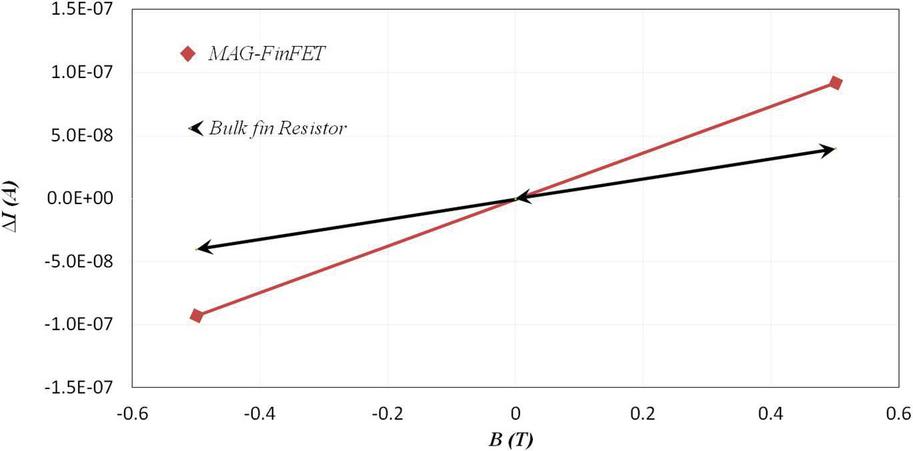
Figure 17 Comparisons of magnetic responses between bulk fin resistor and MAGFinFET.
To compare the two structures for magnetic field detection, the structures in Figures 8(a) and 8(b) were used in study. The fin resistor structure that is shown in the Figure 8(b) uses 10 cm n-type semiconductor instead of the induction channel under gate. The geometric variables in both structures have the same values as nm, nm, and nm. Drain and source act as the ohmic contacts of the fin resistor. Both devices are biased with a constant current of 100 A the magnetic field given in the range 0–0.5 T in the z direction and – z direction.
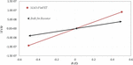
The results of the magnetic response are shown in Figure 17. The relationship between and B, the two structures, is linear throughout the range. The relative sensitivity of the MAGFinFET and fin resistor was 190.65 and 153.50 T, respectively. The relative sensitivities of the other parameter devices are summarized in Table 1. The sensitivity of the MAGFinFET structure is greater than that of the bulk fin resistor and the greater the value as the fin length L, width F and height F increases.
Table 1 Comparison of relative sensitivities () between MAGFinFET and fin resistor
| Sensitivity | ||||
| \backslashboxParameter | (T) | (T) | (T) | Bulk Resistor (T) |
| 10 | 0.00182 | 0.00106 | 0.00310 | 0.00079 |
| 20 | 0.00186 | 0.00277 | 0.00364 | 0.00110 |
| 30 | 0.00190 | 0.00396 | 0.00386 | 0.00153 |
| 40 | 0.00197 | 0.00427 | 0.00409 | 0.00162 |
| 50 | 0.00201 | 0.00468 | 0.00415 | 0.00180 |
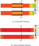
Figure 18 shows the top view of the current density distribution along the cross-section A-A in Figure 8. The above figures of Figure 18(a) and 18(b) are the cases for the non-magnetic field and the figures below are the cases for applied magnetic field 0.5 T. As the results, the difference in the current density of the MAGFinFET structure is clearly visible. On the other hand, it was difficult to distinguish between the cases of non-magnetic field and applied magnetic field in the bulk fin resistor structure.
Figure 19 is the front view of the current density distribution at the cross-section along the A-A near drain in Figure 18 between the MAGFinFET structure and the bulk fin resistor. The middle image shows the case of the absence of a magnetic field, while the left and right pictures are the cases with – 0.5 and 0.5 T magnetic fields, respectively. Similarly, to the top view in Figure 18, the difference in current density can be observed between the cases of applying the magnetic field and not applying the magnetic field of the two structures.
The bulk fin resistive structure is more difficult to observe the difference in current density. In the MAGFinFET structure, the current density is densely located at the both sides and upper fin channels under gate. The middle space charge area has a lower current density and there a leakage current on the bottom substrate under the oxide.
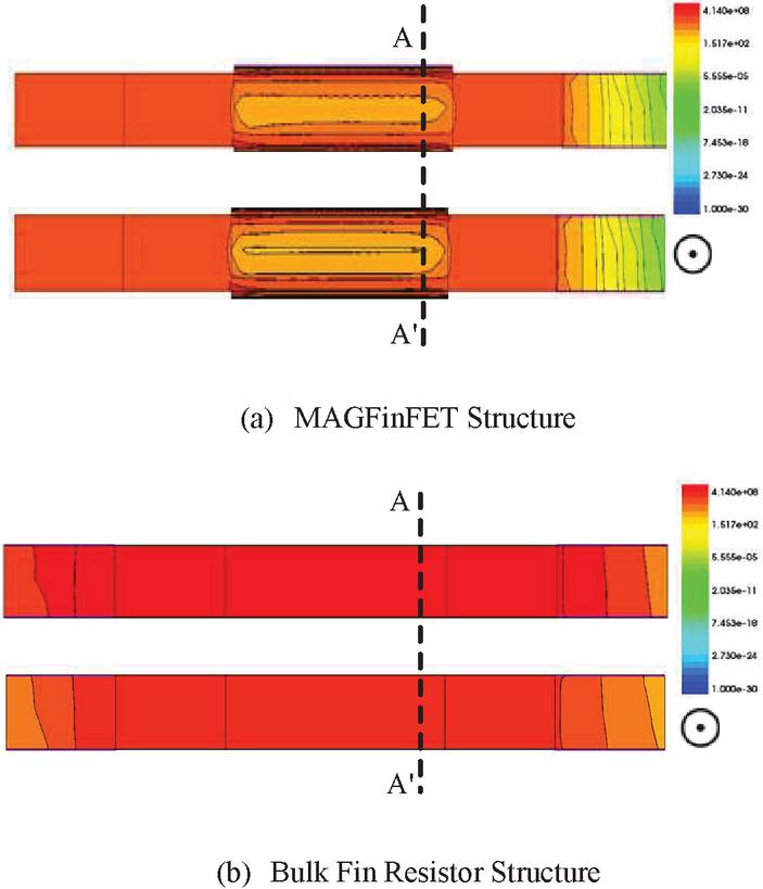
Figure 18 Comparison of top view of current density distribution of MAGFinFET and channel resistor structure nm.
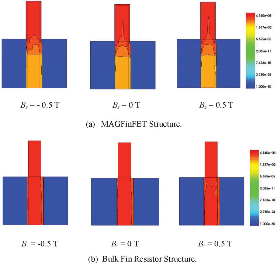
Figure 19 Front view of channel current density near drain.
In a bulk fin resistor structure, the current density is evenly distributed across the substrate. From Figures 18 and 19, it can be seen that the region under the gate has the most changes in current density according to the magnetic field in the structure and therefore, the MAGFinFET structure has a higher sensitivity than the bulk fin resistor structure.
The results of channel length study affecting the magnetic field detection of the device in Figure 11 shows that the longer the channel, the better the detection sensitivity in the range of 10 to 50 nm. It is linear as shown in Table 1. From Equation (2) of a conventional MAGFET device, it can be seen that the MAGFinFET device also corresponds to this equation. The longer the path distance, the greater the deflection distance to the drain with the same deflection angle (), in which case, both the MAGFET and MAGFinFET structures correspond. The deflection of electron currents between short and long channel is shown in Figure 20(a).
When receiving the same bias current and magnetic field, longer channel sees more electron currents tilt toward to D. Even though Equation (2) says that long L is good, but keep in mind that by using the current mode Hall effect, the length-to-width ratio should be small first to cause current deviations. The critical length so called deflection length is the length that, if the design is less than this value, the current deflection is lower.

Figure 20 Current deflections of various comparable parameters of MAGFinFET.
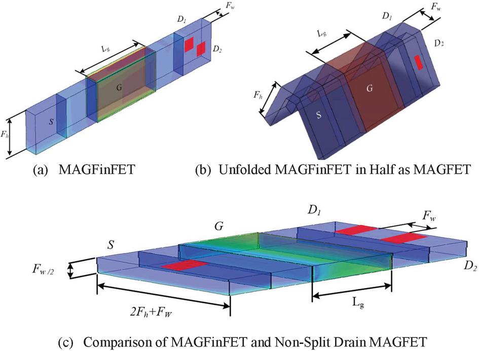
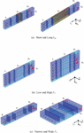
Figure 21 Structure comparison of MAGFinFET and non-split drain MAGFET.
For the fin height F of a MAGFinFET, it is compared to that of a conventional MAGFET channel width W in Figure 2. It can be imagined that the 3-D structure MAGFinFET is cut in half and flattened into a 2-D flattening structure, as shown in Figure 21(a), (b) and (c). The dimension in flattened 2-D MAGFinFET can be illustrated in Figure 21(c). The channel width can be considered as , channel length as L and bulk thickness as . The L/W ratio values in Equation (2) should be large and thus the current difference is large. This means that the MAGFET channel, current mode Hall structure, should be designed with short and wide values in order to causing the angle of deflection, or Lorentz’s angle to be higher. However, the results in Figure 13 have shown that the higher the fin height F, the larger since the MAGFinFET is a 3-D structure.
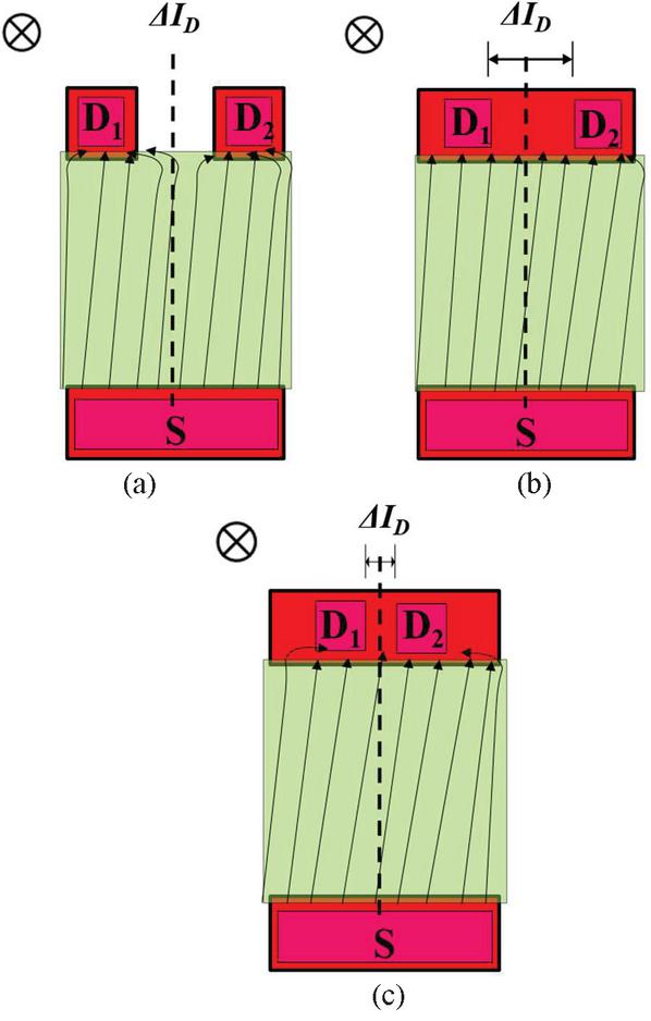
Figure 22 The model of current deflection of (a) split drain MAGFET, (b) non-split drain MAGFET and (c) non-split drain with close contacts.
The fin height F of MAGFinFET that is comparable to the W width in the planar structure of MAGFET does not cause the deflection angle greater. The height of the fin F increases the electron current density distribution cross-section area as shown in Figure 20(b). When the same amount of constant current and are considered, the amount of electron deflection has the more deflected electron current at the higher F. It has been shown in Figure 13.
As for the fin width F in a MAGFinFET structure, it can be compared to the distance d between the contacts D1 and D2 of the non-split drain MAGFET structure in Figure 2(b) or in unfolded MAGFinFET in Figure 21(c). Non-split drained structure in the Figure 2(b) will get a more I than that of a split drain structure. In the split drain MAGFET structure, the current deflection will not be continuous resulting in some loss in the gap between the drains as shown in Figure 22(a). The non-split drain structure provides a current deflection continuous from the channel into the drain without loss at the gap, as shown in Figure 22(b). However, in a non-split drain structure, the distance between the contacts is of the highest importance for the output . If the distance between contacts in drain is close, then the current difference form deflection between D1 and D2 is less than the distance between the longer contacts as shown in Figure 22. Therefore, the result from Figure 14 shows that when fin width F is wider, it means that it has the longer the distance between the contacts so the current difference area will be larger. The drain current is higher as the F is wider. As discussed above, channel length L, fin height F, fin width F are linearly related to the differential current. Therefore, the equation of of MAGFinFET can be written according to Equation (2) as follow
| (6) |
where 2 is from double channel, is current difference, is channel mobility, is channel length, is fin hight, is fin width, is correction geometry factor, is the drain biased current and B is magnetic field density.
5 Conclusion
A new type of MAGFinFET device was introduced. Device structure is based on modern FinFET device structure. It consists of a source, a gate and a drain with two contacts on both sides for current difference. The operation uses the principle of deflecting the current induced by the vertical magnetic field, causing the current difference. Variations on the geometric parameters of the device are simulated for the high performance of electrical characteristics and sensitivity. It can be seen that the larger channel length, fin height and fin width are, the greater the current difference is. Relative sensitivity has the highest value 0.00201 T at channel length 50 nm. Fin height and fin width of 50 nm give the highest sensitivity of 0.00468 T and 0.00415 T respectively. MAGFinFET based magnetic sensor can be integrated in Integrated Circuits (ICs) by modern standard nanofabrication technology. MAGFinFET can be applied in many fields such as low power consumption appliances, traffic density monitoring and control system in the form of wireless sensor networks as part of mobile multimedia industry.
Acknowledgements
The authors would like to thank King Mongkut’s Institute of Technology Ladkrabang for support of this research.
References
[1] Lenz and A.Edelstein, ‘Magnetic Sensors and Their Application’, IEEE Sensors Journal, Vol. 6, No. 3, 2006, pp. 631–649.
[2] P. Ripka, ‘Security applications of magnetic sensors’, Journal of Physics: Conference Series 450 (2013).
[3] C. P. Gooneratne, B. Li and T. E. Moellendick, ‘Downhole Applications of Magnetic Sensors’, Sensors 2017, 17.
[4] Marina Díaz-Michelena, ‘Small Magnetic Sensors for Space Applications’, Sensors 2009, pp. 2271–2288.
[5] M. Hott, P. A. Hoeher and S. F. Reinecke, ‘Magnetic Communication Using High-Sensitivity Magnetic Field Detectors’, Sensors, 2019.
[6] S.Y. Cheung, S. Coleri, B. Dundar, S. Ganesh, C. W. Tan, P. Varaiya, ‘Traffic Measurement and Vehicle Classification with Single Magnetic Sensor’, Journal of the Transportation Research Board, Vol. 1917 Issue 1, 2005, pp. 173–181.
[7] H. S. Fimbombaya, N. H. Mvungi, N. Y. Hamisi and H. U. Iddi, ‘Performance Evaluation of Magnetic Wireless Sensor Networks Algorithm for Traffic Flow Monitoring in Chaotic Cities’. Modelling and Simulation in Engineering Vol. 2018, Article ID 2591304, 11 pages.
[8] V. Velisavljevic, E. Cano, V. Dyo and B. Allen, ‘Wireless Magnetic Sensor Network for Road Traffic Monitoring and Vehicle Classification’. Transport and Telecommunication, 2016, Vol. 17, No. 4, 274–288.
[9] E. Stankevich, I. Paramonov, I. Timofeev, ‘Mobile Phone Sensors in Health Applications’, 12th Conference of Open Innovations Association (FRUCT), 2012.
[10] H. Heidari, E. Bonizzoni, U. Gatti, F. Maloberti and R. Dahiya, ‘Optimal geometry of CMOS voltage-mode and current-mode vertical magnetic hall sensors,’ 2015 IEEE Sensors, 2015, pp. 1–4.
[11] R.S. Popovic, Z. Randjelovic, and D. Manic, ‘Integrated Hall-effect magnetic sensors,’ Sensor and Actuator A, vol. 91, pp. 46–50, 2001.
[12] Z.B. Randjelovic, M. Kayal, M., R. Popovic, and H. Blanchard, ‘High sensitive Hall magnetic sensor microsystem in CMOS technology’, IEEE Journal of Solid-State Circuits, vol. 37, pp. 151–158, 2002.
[13] H. Blanchard, M.F. De, B.J. Hu, R.S. Popovic, ‘Highly sensitive Hall sensor in CMOS technology,’ Sensor and Actuator A, vol. 82, pp. 144–148, 2000.
[14] R. Nakachai, A. Poyai and T. Phetchakul. ‘Non-Split Drain MAGFET’ 5th International Conference on Engineering, Applied Sciences and Technology (ICEAST), 2019.
[15] G.F. Santillan-Quinonez, V. Champac and R.S. Murphy, ‘Exploiting magnetic sensing capabilities of Short Split-Drain MAGFETs’, Solid-State Electronics 54 2010, pp. 1239–1245.
[16] R. Rodríguez-Torres and E.A. Gutiérrez-Domínguez, ‘Analysis of Split-Drain MAGFETs’, IEEE Transactions on Electron Devices, Vol. 51, No. 12, December 2004, pp. 2237–2245.
[17] D. Hisamoto, L. Wen-Chin, J. Kedzierski, E. Anderson, H. Takeuchi, K. Asano, et al., ‘A folded-channel MOSFET for deep-sub-tenth micron era,’ in International Electron Devices Meeting 1998. Technical Digest (Cat. No.98CH36217), 1998, pp. 1032–1034.
[18] J.-P. Colinge, FinFETs and Other Multi-Gate Transistors: Springer Science and Business Media, 2008.
[19] Ghani, T., et al., ‘A 90 Nm High Volume Manufacturing Logic Technology Featuring Novel 45 nm Gate Length Strained Silicon CMOS Transistors’, IEDM Technical Digest. 2003, pp. 978–980.
[20] D. James, ‘Intel Ivy Bridge unveiled -The first commercial tri-gate, high-k, metal-gate CPU,’ in Proceedings of the IEEE 2012 Custom Integrated Circuits Conference, 2012, pp. 1–4.
[21] C. Pamonchom, R. Nakachai, C. Sutthinet, A. Poyai and T. Phetchakul ‘Magnetic FinFET (MAGFinFET)’ 16th International Conference on Electrical Engineering/Electronics, Computer, Telecommunications and Information Technology (ECTI-CON), 2019.
[22] S. Faramehr, B. R. Thomas, N. Janković, J. E. Evans, M. P. Elwin and P. Igić, ‘Analysis of GaN MagFETs compatible with RF power technology,’ 2018 41st International Convention on Information and Communication Technology, Electronics and Microelectronics (MIPRO), 2018, pp. 0050–0053.
[23] Hasan S M R., ‘A novel 0.7 V high sensitivity complementary differential MAGFET sensor for contactless mechatronic applications.’, Sensors and Actuators A: Physical, 2010, 163(1): 138.
[24] R. S. Popovic, Hall Effect Devices: magnetic sensors and characterization of semiconductors, 2 ed.: CRC Press, 2004.
[25] R. Nakachai, A. Poyai, T. Phetchakul, ‘High Sensitivity Non-Split Drain MAGFET for Wireless Sensor Networks’, Journal of Mobile Multimedia, Vol. 16_1–2, 2020, pp. 45–64.
[26] C. Han, X. Shi, Q. Huang, ‘Optimization of short channel effect and external resistance on small size FinFET for different threshold voltage flavors and supply voltages’, Microelectronics Journal 85 (2019) 1–5, Elesvier.
[27] B. Ullmann, T. Grasser, ‘Transformation: nanotechnology—challenges in transistor design and future technologies’, Elektrotechnik & Informationstechnik, 2017, pp. 349–354.
[28] C. Lecuyer, ‘Making Silicon Valley: Innovation and the Growth of High Tech’, pp. 1930–1970, MIT Press, 2006, ISBN 978-0262122818.
[29] R.K. Ratnesh, M.S. Mehata, ‘Synthesis and optical properties of core-multi-shell CdSe/CdS/ZnS quantum dots: surface modifications’, Optical.Materials, vol. 64, 2017, pp. 250–256.
[30] TCAD Sentaurus Manual vol. L-2016.03: Synopsys Inc, 2016.
[31] C. K. Maiti, Introducing Technology Computer-Aided Design (TCAD), 2017.
[32] Y.-C. Wu, Jhan, Yi-Ruei, 3D TCAD Simulation for CMOS Nanoeletronic Devices: Springer Nature, 2018.
Biographies

Khine Thandar Nyunt Swe received the B.E. degree in electronic engineering from Technological University (Magway), Myanmar in 2013 and the M.E. degree in electronic engineering from Yangon Technological University, Yangon, Myanmar in 2017. Her research interests are in digital image processing, semiconductor devices and sensors.

Chanvit Pamonchom received the B.S. degree in Bachelor of Engineering in Mechatronics Engineering Rajamangala University of Technology Rattanakosin, Nakhon Pathom, Thailand in 2015 and the M. E. degree in electronic engineering from King Mongkut’s Institute of Technology Ladkrabang, Bangkok, Thailand in 2021. His research interest areas are electronics circuit design, computer programming, medical instruments, robotics, semiconductor devices, and semiconductor sensors.

Amporn Poyai received the B.Sc. degree in physics from Silpakorn University, Bangkok, Thailand in 1991, the M.S. degree in electrical engineering from King Mongkut’s Institute of Technology Ladkrabang, Bangkok, Thailand in 1994, and the Ph.D. degree in electrical engineering from Katholieke University of Leuven, Leuven, Belgium in 2002. His research is emphasized on design, simulation, fabrication and characterization of semiconductor device, microfabrication technology and integrated circuit. He worked at Thai Microelectronic Center (TMEC) and now he is currently working at Design & Engineering Consulting Service Center (DECC) as part of the National Science and Technology Development Agency (NSTDA), Thailand.

Toempong Phetchakul received the B. S. degree in electronic engineering in 1989, the M. S. degree in electrical engineering in 1992 from King Mongkut’s Institute of Technology Ladkrabang, Bangkok, Thailand and the D. Eng degree in solid state device engineering from Tokai University, Japan in 1997. His research interests are in design, simulation, fabrication and characterization of semiconductor device, semiconductor sensors on integrated circuit. He is currently working at the Department of Electronics, School of Engineering, King Mongkut’s Institute of Technology Ladkrabang, Bangkok, Thailand.
Journal of Mobile Multimedia, Vol. 18_4, 1301–1332.
doi: 10.13052/jmm1550-4646.18416
© 2022 River Publishers