Implementation of Low Power Generic 2D FIR Filter Bank Architecture Using Memory-based Multipliers
Venkata Krishna Odugu1,*, C. Venkata Narasimhulu2 and K. Satya Prasad3
1CVR College of Engineering, Hyderabad, and Research Scholar, JNTUK, Kakinada, India
2Lords Institute of Engineering & Technology, Hyderabad, India
3Retired Professor, ECE, JNTUK, Kakinada, India
E-mail: venkatakrishna.odugu@gmail.com
*Corresponding Author
Received 08 July 2021; Accepted 21 September 2021; Publication 11 January 2022
Abstract
In this paper, a generic filter bank architecture for 2D FIR filter is proposed using block processing, symmetry in the filter coefficients, and memory-based multipliers. The different symmetry filters are considered as sub-filters of the filter bank to decrease the number of multipliers and the desired filter can be selected using control logic to reduce the power consumption. The block processing is incorporated to increase the throughput of the filter. Due to this block processing, memory sharing and memory reuse are achieved to optimize the architecture in terms of area, memory, and power. In each filter, the conventional multipliers are replaced with Distribute Arithmetic (DA) based memory multipliers to decrease the delay, power, and area of each sub-filter. The proposed design is coded by Verilog HDL and synthesized using Cadence Genus tools in 45 nm technology. The physical design is carried out using Cadence Innovus tools. The proposed design results are compared with state-of-the-art works.
Keywords: Low power VLSI design, block processing, parallel processing, symmetry filter, 2D FIR, and memory-based multiplier.
1 Introduction
The two-dimensional (2D) digital filters are widely used in many image processing applications such as biometric systems, image restoration, image enhancement, face recognition, and pattern recognition systems, etc. [1, 2]. The Finite Impulse Response (FIR) is mostly used for image processing applications rather than Infinite Impulse Response (IIR) filters because of simple to design and more stable. The 2D FIR filter architecture implementation in VLSI is a challenging task for researchers. The low power, high speed, and compact area architecture are always preferable for the above applications. The Application Specific Integrated Circuit (ASIC) design-based dedicated architectures need to be implemented for real-time applications.
1.1 Literature Review
Many algorithms to design the 2D FIR filters and many types of architectures of 2D FIR filters are proposed in the literature. Few of them are reported in this paper and motivated from this to implement an efficient 2D FIR filter architecture. The 2D FIR filter architectures using separable and non-separable concepts with block-processing are proposed in [3]. In this paper, generic separable, generic non-separable, and unified 2D FIR filter architectures with various symmetry filters as sub-blocks are implemented with less memory. The low power memory-efficient 2D FIR filter architecture is implemented using high speed and power-efficient Carry Look Ahead (CLA) adders in the paper [4]. A new approach-based FIR filter systolic architecture is proposed without block processing by Vinitha et al. [5]. The symmetry properties can reduce the computations in systolic architectures [6, 7]. In these works, the 2D IIR filter architectures with various symmetry are proposed. Four types of power-efficient symmetrical 2D IIR filters and multimode architectures are also implemented. They are focused on critical path and symmetry only, but single input and single output approaches are only presented.
In the above existing works, power hunger conventional multipliers are used. The complex multiplier block in the filters is replaced with the Distribute Arithmetic (DA) technique. In recent years, DA techniques have attained great importance in the FIR filter implementation to reduce the complexity of architecture with high throughput and regularity. Kumar et al. [8, 9] proposed block-based 2D FIR filter architectures and 2D IIR filter architectures using the DA method. Recently, Odugu et al. [10] proposed novel low complexity 2D FIR filter architectures using Canonical Signed Digit (CSD), Horizontal Common sub-expression Elimination (HCSE), and Vertical Common sub-expression Elimination (VCSE). The design of filters with circular symmetry is presented and optimized architectures are implemented using benefits in the CSD representation of filter coefficients. In this work, the multiplierless 2D FIR filters are implemented without any block processing for circular symmetry.
Multiplier less DA-based FIR filters are presented in [11, 12]. In this work, the review of DA methods for efficient and cost-effective structures of FIR filters is explained. Park et al. [13] have been proposed an efficient DA-based reconfigurable filter structure. Mohanty et al. [14] have been introduced a block-based 1D filter, which is based on a completely DA based reconfigurable FIR filter for Software Defined Radio (SDR) channelizer for narrow banding filter applications, in which block processing and DA technique have been used to improve the sampling rate and to reduce the power consumption. The memory sharing is introduced between the consecutive DA blocks to get area – delay – power-efficient 1D FIR filter.
Meher et al. [15, 16] proposed a new approach in the memory-based multipliers using LUT. In this paper, odd multiples are only stored in LUT and even multiples of coefficients are generated using shifting. Memory-based LUT multipliers are considered for the implementation of 1D FIR filters and the results are compared with DA-based FIR filters. This LUT-based multiplication process is discussed by Vinitha et al. [17], using even multiples storage methods. The encoder and shifting blocks are eliminated and hardware requirement is diminished. The Dual-port LUT concept is acquainted rather than single-port LUT multiplication by D. F. Chiper et al. [18]. Sharma et al. [19] presented a modified (Odd Multiples Storage) OMS-LUT design for memory-based multiplication. Recently, Odugu et al. [20] proposed a novel 2D FIR filter using approximation multipliers. These multipliers are designed using approximate 4:2 compressors to improve the design metrics of multiplier and filter. Significant improvements are achieved in terms of power, area, and delay without compromising accuracy. Few novel points are considered from the literature, and a new memory-based multiplication process is carried out in the proposed 2D FIR filter banks.
In the literature, there is no combination of block processing and symmetry in 2D FIR filters. In this paper, block processing is incorporated to attain memory reuse and improve the throughput. Four types of symmetry coefficients, such as diagonal symmetry, four-fold symmetry, quadrant symmetry, and octagonal symmetry are utilized to decrease the number of multipliers in filter structure and using these symmetries circular, diamond, and fan-type filters can be designed [21]. Further, the complexity of the remaining multipliers is low area memory-based LUT-DA multipliers.
The contributions of this work are as follows:
➢ Block processing is introduced to improve the throughput and to reuse the memory registers.
➢ Four types of symmetries for 2D FIR filters are analyzed and considered to reduce the number of multipliers.
➢ Conventional multipliers are replaced with memory-based LUT multipliers to decrease the power consumption and area of the arithmetic modules of each symmetry filter.
➢ A generic filter bank architecture is implemented in the ASIC design platform.
The paper is organized as follows: Section 2 describes the design concepts of block processing and different symmetry in coefficients of 2D FIR filter. In Section 3, the proposed filter bank architecture is described and the complete architectures of a general filter of 2D FIR filters using enhanced dual-port LUT-based multipliers. The comparison of results with existing architectures is explained in Section 4. The paper’s conclusions and remarks are discussed in Section 5.
2 Block Processing or Parallel Processing in 2D FIR Filter Architecture
In the digital filters, the block processing concept increases the throughput of the architecture. If the input block size is L, then the filter produces ‘L’ outputs per one iteration, which means L times throughput is increased. The general expression of the 2D FIR filter is given by Equation (1),
| (1) |
where is a coefficients matrix for 2D FIR filter for order N. If the block size is ‘L’, then the kth block output of the 2D FIR filter is given by Equation (2).
| (2) |
Where is the overall filter output and it is given by Equation (3).
| (3) |
and is an intermediate vector and it can be written as an Equation (4).
| (4) |
Here, is the product of the coefficients matrix with the input matrix and represented by Equation (5),
| (5) |
Where, is part of the input matrix is shown by Equation (6), from th row of the input image matrix.
| (6) |
The filter coefficients matrix is denoted by Equation (7),
| (7) |
The internal vectors of the matrix are the inner product of coefficients matrix and is the th row of is shown in Equation (8).
| (8) |
The 2D FIR filters such as fully direct form, fully transposed form, direct-transposed form, and transposed-direct form structures are available to implement the architecture. From these, a fully direct form of 2D FIR filter is considered in this paper for memory reuse. The memory requirement is less for a fully direct 2D FIR filter because it is dependent on input word length only. This feature can be used to reduce the memory storage in 2D filters. The higher input block size is increases the hardware complexity in the architecture and also improves the throughput of the filter. The overhead area can be compensated using different symmetry of coefficients in the filters.
2.1 Different Symmetry Types of 2D FIR Filters
The multiplier is a complex and most power-consuming block in any filter structure, which can be reduced using specific symmetry in filter coefficients. In this paper, four types of symmetries such as diagonal, four-fold rotational, quadrantal, and octagonal symmetries in the 2D filter coefficients are incorporated in the filter bank as sub-filters blocks to reduce the area, delay, and power. The four symmetries in the 2D FIR filter are designed by the following transfer functions [6]. The output to input relation of diagonal symmetry filer is given by Equation (9),
| (9) |
The transfer function of the four-fold rotational symmetry filter is represented by Equation (10).
| (10) |
where, , and ,
The transfer function of the quadrantal symmetry filter is expressed as Equation (11).
| (11) |
The symmetry in octagonal filter coefficients is given by for all . The overall transfer function of the octagonal filter is shown in Equation (12).
| (12) |
The coefficient matrix of general filter (without symmetry) and 2D diagonal, four-fold rotational, quadrantal, and octagonal-FIR filter coefficients for order N 4 is shown in the 4 4 matrices in Figure 1.
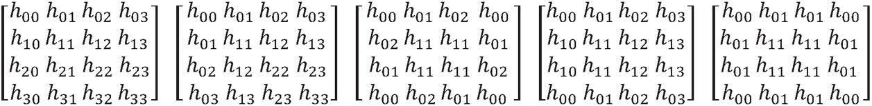
Figure 1 (a) Coefficients of general filter (b) coefficients of diagonal symmetry (c) coefficients of four-fold rotational symmetry (d) coefficients of quadrantal symmetry (e) coefficients of octagonal symmetry filters.
3 Proposed Filter Bank Architecture of 2D FIR Filters
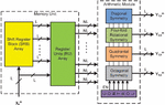
In this work, four efficient symmetrical 2D FIR filters are analyzed and used to implement one generic filter bank architecture. This generic 2D FIR filter architecture consists of a storage memory unit and arithmetic module block. The memory unit is mutually shared by all the sub-filters of the arithmetic module. The sharing of a common memory unit decreases the overall memory requirement of the filters. The proposed 2D FIR filter bank architecture is shown in Figure 2 for order N and block size is L. It consists of four filter modules with common Shift Register Block (SRB) Array and Register Unit (RU) array, which are used for memory reuse and memory sharing to reduce the storage memory of the filter bank.
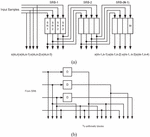
From a two-dimensional input matrix with a size of M M, the block of ‘L’ current samples is given to the SRB array. These block input samples are passing through N 1 shift register blocks of the SRB array and each SRB consists of L number of registers is shown in the Figure 3(a). Further, the outputs of all SRB blocks and current samples are applied to the N number of corresponding RUs of RU-Array. The RU is constructed by N 1 D Flip-Flops, which gives the required past and present samples for the systolic operation of block processing with memory reuse. The RU produces NL samples as shown in the Figure 3(b). The Total N NL number of samples are produced by N number of RUs and applied commonly to each sub-arithmetic module of the filter bank.
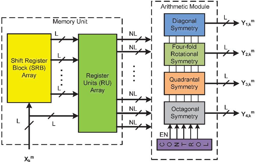
Figure 2 The proposed architecture of block-based 2D FIR filter bank.
The common storage memory unit is the advantage of the filter bank and it is shared by all individual filters. Each L block-sized 2D FIR sub-filter required the memory of (M N) (N 1). If four filters are individually implemented, then the total memory is required to be 4 (M N) (N 1). But, the proposed filter bank needs the memory of (M N) (N 1), which is required for one filter. So, the filter bank saves the memory 4 times due to the memory sharing concept.
In the proposed filter bank architecture, to select the desired filter with specific symmetry a control logic block is required. Whenever one filter is chosen for processing the input samples and the other filters must be shut off and saves the power consumption per output. Otherwise, all filters also can be selected for parallel processing of all symmetry filters. The control logic enables signals to select the desired symmetry sub-filter as well as the parallel realization in the arithmetic module block. Each sub-module gives L number of outputs corresponding to the L number of input samples per one iteration.
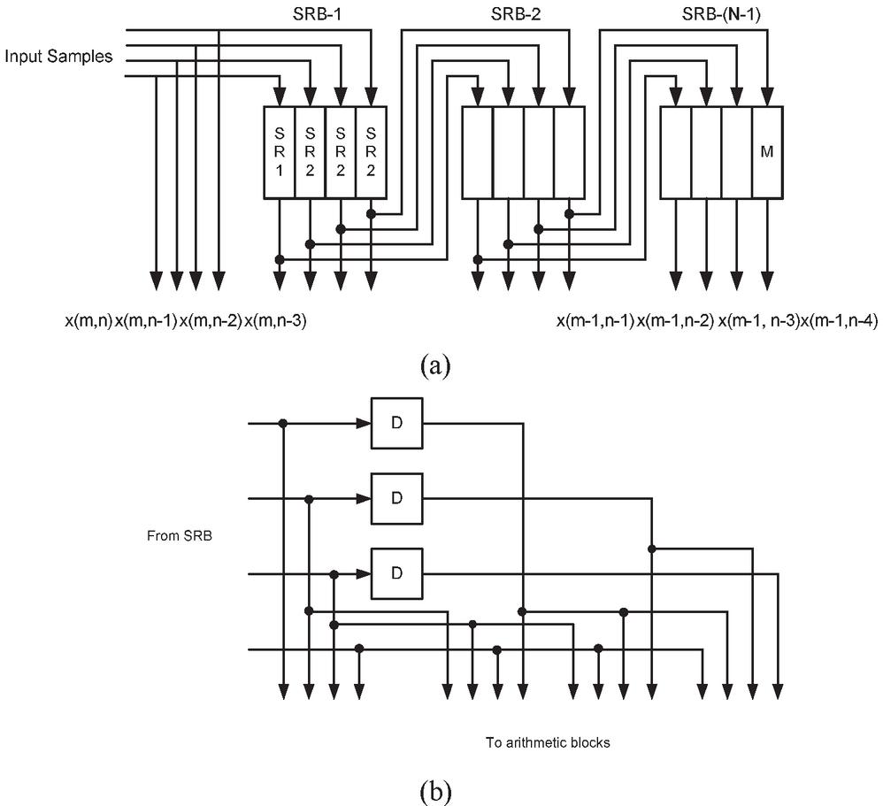
Figure 3 (a) The structure of the SRB array for N 4 with L 4 (b) Internal structure of RU for N 4 and L 4.
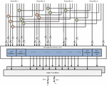
3.1 Arithmetic Module of Sub-filter
The arithmetic module block of the filter bank consisting of four symmetry filter sub modules. Each sub-arithmetic module is constructed by multipliers, adders, and adder tree blocks. The internal structure of the diagonal symmetry 2D FIR filter arithmetic module is shown in Figure 4 as an example. The multipliers are most complex blocks than adder blocks. So, optimization is required for the implementation of multipliers. In this paper, the multiplication process is done by the DA technique using memory-based or LUT-based multipliers.
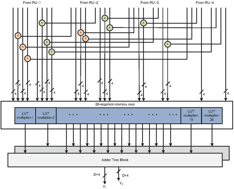
Figure 4 The internal structure of the arithmetic module of the diagonal symmetry filter for N 4 and L 4.
3.2 LUT Based Memory Multiplier
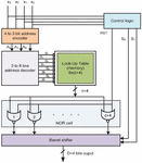
The LUT is considered as a memory to store the values of precomputed filter coefficients. Based on the applied input, the corresponding address is fetched and stored coefficient values are given by LUT. The output values of LUT are appropriately shifted and accumulated is called DA multiplication. In this multiplication process, one is a fixed coefficient and the other one is a variable input sample. Consider ‘x’ is a binary input with the length of W-bits, and ‘H’ is a filter coefficient constant with the length of D-bits. The LUT should store the 2 possible values. In the conventional LUT-based multiplication method, 2 words are used to design the LUT to store all possible pre-computed partial products.
The LUT size corresponding to the number of input sample bits can be reduced to (2/2) words. This is achieved by storing the only odd multiples of coefficient H in LUT. Next, the even multiples of coefficients are derived by using the left shift operations to the odd multiples produced by LUT memory. This method of odd multiples storage and even multiplies generation is described in Table 1 for 4-bits of the input sample. Here, the 8-address locations are used to store the odd multiples of coefficient H, such as H, 3H, 5H, 7H, 9H, 11H, 13H, and 15H. and the even multiples are estimated by the left shift operations of H, such as 2H, 4H, 8H by 1, 2, and 3 times left shift operations to H respectively. Next, 6H and 12H products are determined by a left shifting of 3H, and the remaining 10H is getting from 5H, and 14H is derived from 7H respectively. The product output corresponding to the input sample all zeros i.e is determined by resetting the LUT.
Table 1 Multiplication approach of Memory-based multiplier [16]
| Value to be | Actual Input | Required | Number of | Control | ||
| Address | Word | Stored | Bits (W) | Product | Shifts | Lines |
| AAA | Name | in LUT | xxxx | Value | Required | SS |
| 0 0 0 | W0 | H | 0 0 0 1 | H | 0 | 0 0 |
| 0 0 1 0 | 2 H | 1 | 0 1 | |||
| 0 1 0 0 | 2 H | 2 | 1 0 | |||
| 1 0 0 0 | 2 H | 3 | 1 1 | |||
| 0 0 1 | W1 | 3H | 0 0 1 1 | 3H | 0 | 0 0 |
| 0 1 1 0 | 2 3H | 1 | 0 1 | |||
| 1 1 0 0 | 2 3H | 2 | 1 0 | |||
| 0 1 0 | W2 | 5H | 0 1 0 1 | 5H | 0 | 0 0 |
| 1 0 1 0 | 2 5H | 1 | 0 1 | |||
| 0 1 1 | W3 | 7H | 0 1 1 1 | 7H | 0 | 0 0 |
| 1 1 1 0 | 2 7H | 1 | 0 1 | |||
| 1 0 0 | W4 | 9H | 1 0 0 1 | 9H | 0 | 0 0 |
| 1 0 1 | W5 | 11H | 1 0 1 1 | 11H | 0 | 0 0 |
| 1 1 0 | W6 | 13H | 1 1 0 1 | 13H | 0 | 0 0 |
| 1 1 1 | W7 | 15H | 1 1 1 1 | 15H | 0 | 0 0 |
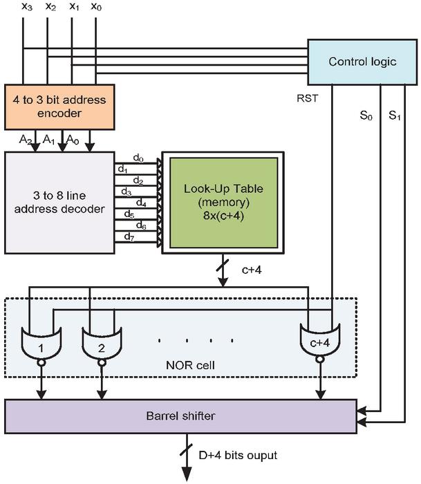
Figure 5 Structure of memory-based LUT multiplier.
The LUT-based memory multiplier according to Table 1 is shown in Figure 5. It consists of a 4-to-3 encoder, a 3-to-8 decoder, control logic to produce Reset (RESET), and the control lines {S0, S1}to produce shifts required for the computation of even multiples of coefficients such 2H, 4H, 8H, 10H, 12H, and 14H. Two bits are enough to produce the maximum of 3 shift operations, so two control signals are taken in the structure. Extra 4 bits are essential to computing the highest odd multiple value 15H is precomputed and stored in LUT. Eight odd multiples of coefficients with (D 4) bits. The decoder output is the address for the LUT and the corresponding location is read and it is applied to the NOR cell. The NOR cell is designed by D+4 NOR gates with one common input of reset (RESET). The RESET is derived from the applied input sample using a control logic circuit. Next, the NOR cell outputs are shifted using barrel shifter according to the control signals {S0, S1} from the control logic. The barrel shifter has 2 x (D 4) AOI (AND_OR_ INVERT) gates or 21 multiplexers. Finally, the barrel shifter output is the multiplication result of the coefficient and input sample. The Boolean expressions of the 4-to-3 encoder are expressed in Equation (13)(a)–(c),
| (13a) | ||||
| (13b) | ||||
| (13c) | ||||
The control logic signals (RESET and S0, S1) are given by Equation (14)(a)–(c).
| (14a) | ||||
| (14b) | ||||
| (14c) | ||||
4 Results
The proposed filter bank architecture with block processing and symmetry is implemented in the platform of Application Specific Integrated Circuit (ASIC). The proposed filter bank and sub-blocks are coded using Verilog Hardware Description Language (HDL) and validated and synthesized using Cadence Genus tools in 45 nm CMOS generic library. The order of each filter is considered as N 4 with an input block size of L 4. Next, the physical design is done using Cadence Innovus tools. In the physical design, proper floor planning, placement, clock tree synthesis, and routing are carried out for the optimized design.
Table 2 Comparison of performance metrics of filter bank architectures for N 4 and L 4, for input sample bits W 4, 8 and 16
| Type of the | |||||||||
| Filter Bank | Area (m) | Delay (ns) | Power (mW) | ||||||
| Input | |||||||||
| Sample Bits | W 4 | W 8 | W=16 | W 4 | W 8 | W=16 | W 4 | W 8 | W=16 |
| Filter bank with Conventional multipliers | 97288 | 198565 | 256955 | 12.77 | 13.25 | 13.89 | 2.74 | 3.582 | 4.961 |
| Filter bank with LUT multipliers | 89441 | 149925 | 187658 | 4.81 | 5.06 | 6.56 | 1.908 | 2.118 | 2.986 |
For comparison purposes, the filter bank architecture was also implemented using conventional multipliers. The VLSI design metrics such as area, delay, and power consumption of filter banks implemented by conventional multipliers and LUT multipliers are compared in Table 2 for the input sample bits of W 4, 8, and 16.
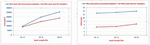
The proposed 2D FIR filter bank architecture using LUT multipliers is attained 27% of area saving than the conventional multipliers based architecture for W 16, N 4, and L 4. The delay of the proposed work is 53% less than the delay of conventional multiplier-based filter bank architecture. The power consumption improvement of the proposed work is 40% obtained than the filter bank with normal multipliers. The graphical representation of the area, delay, and power consumptions of the proposed 2D FIR filter bank architecture with LUT-based multipliers is shown in Figures 6 and 7 respectively.
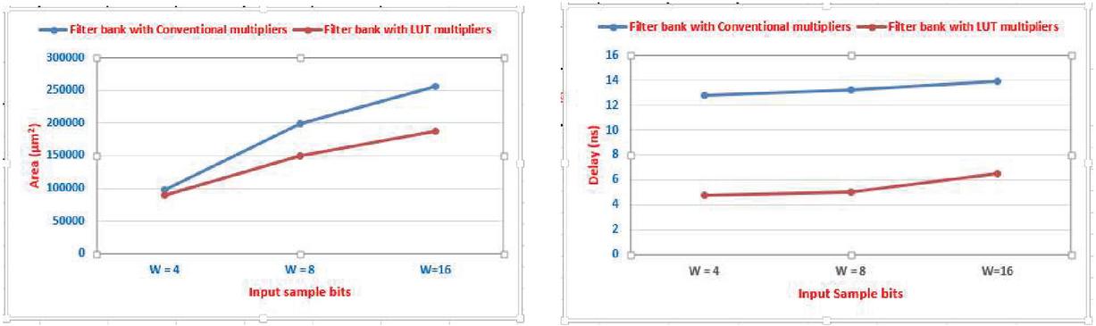
Figure 6 Area and Delay comparison of filter banks for input sample bits W 4, 8, and 16.
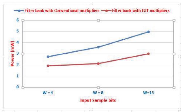
Figure 7 Power comparison of the filter bank architectures with W 4, 8, and 16.
Table 3 Comparison results of proposed filter bank with existing works for N 4 and L 4
| Block | Area | Delay | Power | Area-Delay-Product | PDP | |
| Architecture | Size L | (m) | (ns) | (mW) | (mms) | (mWns) |
| Mohanty [3] | 4 | 791361 | 12.16 | 6.0934 | 9.6 | 74.08 |
| Kumar [8] | 4 | 325825 | 6.53 | 10.05 | 2.124 | 65.6 |
| Kumar [9] | 4 | 233031 | 4.68 | 6.02 | 1.088 | 28.16 |
| Alawad [22] | 4 | 156153 | 11.82 | 2.016 | 1.844 | 23.8 |
| Proposed Filter bank architecture | 4 | 149925 | 5.06 | 2.118 | 0.756 | 10.716 |
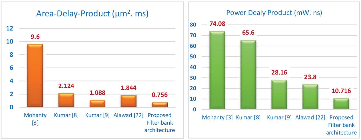
Figure 8 Comparison of ADP and PDP of proposed work with existing works.
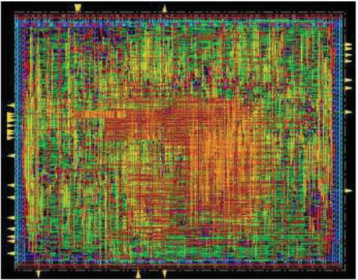
Figure 9 Layout of proposed filter bank architecture for L 2, N 4.
The proposed 2D FIR filter bank is compared with the state-of-the-art works in Table 3. It can be observed that the proposed architecture is improved in terms of area, delay, power, ADP, and PDP than existing architectures. The ADP of the proposed architecture is 12.6 times less than when related to the architecture of Mohanty et al. [3]. The ADP of the proposed architecture is 2.8 times less than the architecture of Kumar et al. [8], 1.43, and 2.43 times lesser than the works of Kumar et al. [9] and Alawad et al. [22] respectively. The PDP of the proposed work is 6.9, 6.12, 2.62, and 2.22 times lesser than the works of Mohanty et al. [3], Kumar et al. [8], Kumar et al. [9], and Alawad et al. [22] respectively. The comparison analysis of ADP and PDP of existing architectures with the proposed 2D FIR filter bank architecture is presented in Figure 8. The final physical layout generated by cadence Innovus tools for the proposed filter bank architecture is shown in Figure 9. The layout area of the proposed 385.6 m 388.8 m.
5 Conclusion
The block-based 2D FIR filter bank architecture is proposed and implemented with four symmetry filters using optimized memory-based Look-up-table (LUT) multipliers. The common memory unit is shared by four symmetry sub filters to reduce the overall memory requirement. The number of multipliers is decreased by incorporating the various symmetries in the filter coefficients of the 2D FIR filter. Memory sharing in the filter bank and memory reuse due to block processing is achieved. Significant Power saving is also obtained due to the control logic used in filter bank architecture to select the desired filter. The complex multiplier blocks are replaced with the memory-based LUT multipliers. The ASIC synthesis results of the proposed architecture for N 4 and L 4 with input sample bits of w 4, 8, and 16 are validated and compared with state-of-the-art works. The proposed architecture of the 2D FIR filter bank outperforms the existing 2D FIR filter architectures in terms of area, delay, power consumption, and memory.
Conflict of Interest
The authors declare that they have no conflict of interest.
References
[1] Sid-Ahmed, M. A. Image Processing: Theory, Algorithms and Architectures (McGraw-Hill, New York, 1995).
[2] Barbu, T. (2010). Gabor filter-based face recognition technique. Proc. Rmanian Acad. Ser. A 11(3), 277–283.
[3] Mohanty, Basant K., et al. (2013). Memory footprint reduction for power-efficient realization of 2-D finite impulse response filters. IEEE Transactions on Circuits and Systems I: Regular Papers 61.1, 120–133.
[4] Odugu, V. K., Narasimhulu, C. V. and Prasad, K. S. (2019). Implementation of low power and memory-efficient 2D FIR filter architecture. International Journal of Recent Technology and Engineering, 8(1), 927–935.
[5] Vinitha, C. S. and Sharma, R. K. (Mar 2019). New approach to low-area, low-latency memory-based systolic architecture for FIR filters. Journal of Information and Optimization Sciences, 40(2), 247–262.
[6] Van, L. D., Khoo, I. H., Chen, P. Y. and Reddy, H. H. C. (2019). Symmetry incorporated cost-effective architectures for two-dimensional digital filters. IEEE Circuits and Systems Magazine, 19(1), 33–54.
[7] Chen, P. Y., Van, L. D., Khoo, I. H., Reddy, H. C. and Lin, C. T. (2010). Power-efficient and cost-effective 2-D symmetry filter architectures. IEEE Transactions on Circuits and Systems I: Regular Papers, 58(1), 112–125.
[8] Kumar, P., Shrivastava, P. C., Tiwari, M. and Mishra, G. R. (2019). High-throughput, area-efficient architecture of 2-D block FIR filter using distributed arithmetic algorithm. Circuits, Systems, and Signal Processing, 38(3), 1099–1113.
[9] Kumar, P., Shrivastava, P. C., Tiwari, M. and Dhawan, A. (2018). ASIC implementation of area-efficient, high-throughput 2-D IIR filter using distributed arithmetic. Circuits, Systems, and Signal Processing, 37(7), 2934–2957.
[10] Odugu, Venkata Krishna, C. Venkata Narasimhulu and K. Satya Prasad. (2020). Design and implementation of low complexity circularly symmetric 2D FIR filter architectures. Multidimensional Systems and Signal Processing, 1–26.
[11] Naga Jyothi, Grande and Sriadibhatla SriDevi. (2017). Distributed arithmetic architectures for fir filters-a comparative review. 2017 International Conference on Wireless Communications, Signal Processing and Networking (WiSPNET). IEEE.
[12] NagaJyothi, G. and Sridevi, S. (2019). High speed and low area decision feedback equalizer with novel memoryless distributed arithmetic filter. Multimedia Tools and Applications, 78(23), 32679–32693.
[13] Park, S. P. Meher, (2014). Efficient FPGA and ASIC realization of a DA-based reconfigurable FIR digital filter. IEEE Trans. Circuits Syst. II Express Briefs, 61(7), 511–515.
[14] Mohanty, B. K., Meher, P. K., Singhal, S. K. and Swamy, M. N. S. (2016). A high-performance VLSI architecture for reconfigurable FIR using distributed arithmetic. Integration, 54, 37–46.
[15] Meher, P. K. (2009, Dec). New look-up-table optimizations for memory-based multiplication. In Proceedings of the 2009 12th International Symposium on Integrated Circuits (pp. 663–666). IEEE.
[16] Meher, Pramod Kumar. (2010). New approach to look-up-table design and memory-based realization of FIR digital filter. IEEE Transactions on Circuits and Systems I: Regular Papers, 57.3, 592–603.
[17] Vinitha, C. S. and Sharma, R. K. (Dec 2019). An efficient LUT design on FPGA for memory-based multiplication. Iranian Journal of Electrical and Electronic Engineering, 15(4), 462–476.
[18] D. F. Chiper, M. N. S. Swamy, M. O. Ahmad and T. Stouraitis. (2005) Systolic algorithms and a memory-based design approach for a unified architecture for the computation of DCT/DST/IDCT/IDST, IEEE Trans. Circuits Syst. I, Reg. Papers, 52(6), 1125–1137.
[19] Sharma, D., Johnson, J. and Sharma, A. (2019). Memory-based FIR digital filter using modified OMS-LUT design. In Applications of Computing, Automation and Wireless Systems in Electrical Engineering (pp. 1007–1017). Springer, Singapore.
[20] Odugu, V. K., Venkata Narasimhulu, C. and Satya Prasad, K. (2021). An efficient VLSI architecture of 2-D finite impulse response filter using enhanced approximate compressor circuits. Int. J. Circ. Theor. Appl., 1–16. doi:10.1002/cta.3114.
[21] Matei, R. (2018). Analytical design methods for directional Gaussian 2D FIR filters. Multidimensional Systems and Signal Processing, 29(1), 185–211.
[22] Alawad, M. and Lin, M. (2017). Memory-Efficient Probabilistic 2-D Finite Impulse Response (FIR) Filter. IEEE Transactions on Multi-Scale Computing Systems, 4(1), 69–82.
Biographies

Venkata Krishna Odugu received B. Tech degree in Electronics and Communication Engineering from Acharya Nagarjuna University, 2004 and Master of Technology with specialization in VLSI System Design from JNTU Hyderabad in 2009 and pursuing Ph.D. from JNTU Kakinada in the area of VLSI Signal Processing. He is having 15 years of teaching experience. He is working as Associate Professor in the department of ECE, CVR College of Engineering Hyderabad. He has published 9 International Journals and 14 National Journals. His interested areas are VLSI Design and VLSI Signal Processing, 2D FIR filters architectures.

C. Venkata Narasimhulu received B.Tech degree in Electronics and Communication Engineering from S V University, Tirupathi in 1995 and Master of Technology in Instrumentation & Control Systems from REC, Calicut in 2000 and Ph.D. from JNTU, Kakinada in 2013 in the area of signal processing. He has published more than 45 technical papers in national and international Journals and Conferences. His interested areas are Signal Processing, Cognitive Radio, Image processing, and medical image processing, etc.

K. Satya Prasad received B Tech. degree in Electronics and Communication Engineering from JNTU College of Engineering, Anantapur, in 1977 and M. E. degree in Communication Systems from Guindy College of Engineering, Madras University, in 1979 and Ph.D. from Indian Institute of Technology, Madras in 1989. He has published more than 150 technical papers in different National & International conferences and Journals and Authored one Textbook. His areas of Research include Communications Signal Processing, Image Processing, Speech Processing, Neural Networks & Ad-hoc wireless networks, etc.
Journal of Mobile Multimedia, Vol. 18_3, 583–602.
doi: 10.13052/jmm1550-4646.1836
© 2022 River Publishers